HAL Id: hal-01052761
https://hal.archives-ouvertes.fr/hal-01052761
Submitted on 28 Jul 2014
HAL is a multi-disciplinary open access
archive for the deposit and dissemination of
sci-entific research documents, whether they are
pub-lished or not. The documents may come from
teaching and research institutions in France or
abroad, or from public or private research centers.
L’archive ouverte pluridisciplinaire HAL, est
destinée au dépôt et à la diffusion de documents
scientifiques de niveau recherche, publiés ou non,
émanant des établissements d’enseignement et de
recherche français ou étrangers, des laboratoires
publics ou privés.
Parametric optical signal processing in silicon
waveguides with reverse-biased p-i-n junctions
Christophe Peucheret, Francesco da Ros, Dragana Vukovic, Kjeld Dalgaard,
Michael Galili, Andrzej Gajda, Lars Zimmermann, Bernd Tillack, Klaus
Petermann
To cite this version:
Christophe Peucheret, Francesco da Ros, Dragana Vukovic, Kjeld Dalgaard, Michael Galili, et al..
Parametric optical signal processing in silicon waveguides with reverse-biased p-i-n junctions. IEEE
Photonics Society 2014 Summer Topical Meeting Series (PHOSST 2014), Jul 2014, Montreal, QC,
Canada. 116-117 (paper TuD4.1), �10.1109/SUM.2014.67�. �hal-01052761�
Parametric Optical Signal Processing in Silicon Waveguides
with Reverse-biased p-i-n Junctions
C. Peucheret
1, F. Da Ros
2, D. Vukovic
2,
K. Dalgaard
2, and M. Galili
21 FOTON Laboratory, CNRS UMR 6082, ENSSAT,
University of Rennes 1 F-22305 Lannion, France
2 Department of Photonics Engineering
Technical University of Denmark DK-2800 Kgs. Lyngby, Denmark e-mail: [email protected]
A. Gajda
3,4, L. Zimmermann
4, B. Tillack
3,4,
and K. Petermann
33 Institut für Hochfrequenz- und
Halbleiter-Systemtechnologien TU Berlin 10587 Berlin, Germany
4 IHP
15236 Frankfurt (Oder), Germany
Abstract—The use of silicon-on-insulator waveguides with free carriers removal using a reverse-biased p-i-n junction for parametric optical signal processing is reviewed. High-efficiency wavelength conversion and phase-sensitive regeneration are reported.
Keywords-nonlinear optical signal processing; silicon nano-waveguides; four-wave mixing; phase-sensitive processes.
I. INTRODUCTION
The use of parametric processes in materials presenting a third order nonlinearity is a well-known technique for the demonstration of optical signal processing functionalities, including wavelength conversion, parametric amplification, optical phase conjugation and regeneration [1]. Such demonstrations have traditionally been performed using highly nonlinear optical fibers (HNLFs) as the nonlinear interaction medium. However, due to their relatively weak nonlinearity, HNLF lengths of the order of several hundred meters are typically required. In such fibers, the efficiency of parametric processes is often limited by stimulated Brillouin scattering (SBS). Furthermore, longitudinal variations of the dispersion may affect the fulfillment of the phase matching condition, hence the parametric device bandwidth. Therefore, even though fiber modules can be made relatively compact, and in spite of the maturity of the HNLF technology, other nonlinear materials have been investigated over the past few years.
Optical planar waveguides made from high-index nonlinear media presenting a higher nonlinear coefficient than silica HNLFs enable compact implementations of parametric devices. In particular, nano-waveguides made from crystalline silicon have been successfully employed for all-optical signal processing [2]. Such devices are compact, may not exhibit strong SBS, and benefit from widely tunable dispersion properties, hence flexibility in fulfillment of the phase matching condition, by engineering the cross-section of the waveguide. However, they suffer from nonlinear loss at telecommunication wavelengths (~1550 nm) due to free-carrier attenuation induced by two-photon absorption (TPA). This limitation can be lifted by employing transverse
reverse-biased p-i-n junctions across the silicon waveguides, where the induced electric field is used to sweep away the carriers generated by TPA, thus reducing their effective lifetime [3].
In this contribution we review some of our recent optical signal processing achievements with such silicon waveguides. In particular, we show how record four-wave mixing (FWM) wavelength conversion efficiencies can be obtained, and how such waveguides can be employed to demonstrate the first on-chip phase-sensitive signal processing in a third order nonlinear medium with continuous wave (CW) pumping.
II. WAVEGUIDES DESIGN AND PROPERTIES
The structure of the silicon-on-insulator (SOI) nano-rib waveguides used in our demonstrations is represented in Fig. 1 [3]. The waveguides, whose dimensions are W = 500 nm, H = 210 nm and s = 50 nm, were fabricated in a BiCMOS foundry using 248-nm lithography. Doped regions were introduced on both sides of the waveguides through implantation of boron and arsenic for the p- and n- region, respectively. The propagation loss, length, TPA coefficient and nonlinear coefficient of the waveguides used in the system demonstrations are 1 dB/cm, 4 cm, 0.5 cm/GW and 280 W-1·m-1, respectively.
III. PHASE-INSENSITIVE PROCESSING
Using the fabricated waveguides, a record CW conversion efficiency of -1 dB (measured at the output of the
Figure 1. Scanning electron microscope picture of the cross-section of a silicon nano-rib waveguide. The doped regions are located 350 nm away on
-35 -30 -25 -20 -15 10 9 8 7 6 5 4 back-to-back idler 0 V bias idler 20 V bias -l o g (BER )
average received power (dBm) b 1549 1550 1551 1552 1553 1554 1555 -80 -60 -40 -20 0 re la ti v e p o w e r (d B ) wavelength (nm) no junction 20 V bias a
Figure 2. (a) Spectra at the output of the Si waveguide w/ and w/o p-i-n junction. (b) BER curves of the idler for different biasing conditions.
waveguide) could be obtained for a coupled pump power of 26 dBm [3]. Low penalty wavelength conversion of a 40-Gbit/s on-off keying modulated input signal was successfully achieved under CW pumping (20-dBm pump power) [4], as shown in Fig. 2. The output conversion efficiencies with a p-i-n juntion and a (reverse) bias voltage of 20 V or 0 V, as well as in an identical reference waveguide without p-i-n junction were -4.6 dB, -8 dB and -26.9 dB, respectively. No error free detection was possible from the weak idler generated without p-i-n junction, while the built-in field of the unbiased junction enabled wavelength conversion with a power penalty of 8 dB (BER=10-9), limited by the poor signal-to-noise ratio of the
idler. In contrast, a penalty of only 0.2 dB was measured under reverse bias, clearly demonstrating the benefit of employing the p-i-n junction.
IV. PHASE-SENSITIVE PROCESSING
Phase-sensitive amplification (PSA) is a powerful technique that exploits parametric effects in order to selectively process the two complex quadratures of the optical field, therefore enabling new functionalities such as phase regeneration [5]. Phase sensitive processing had until now only been demonstrated under practical CW pumping configuration in HNLFs [5] and χ(2) materials [6], as well as
in chalcogenide waveguides [7] and Si photonic crystal (PhC) waveguides, but only under pulsed operation [8].
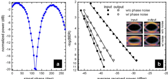
We have recently reported the first demonstration of phase-sensitive processes using an SOI waveguide with reverse-biased p-i-n junction operated in a single-pump degenerate-idler scheme [9]. For these demonstrations, the signal and pumps were obtained from a frequency comb generator to maintain the required coherence between the waves. Under static operation, a phase-sensitive extinction ratio of 20 dB could be obtained for a total pump power of 23.5 dBm [10], as shown in Fig. 3(a). The scheme could be applied to the phase regeneration of a differential phase- shift keying (DPSK) signal modulated at 10 Gbit/s [10]. In the absence of phase noise loading, the phase-sensitive processing induces an implementation penalty of 1 dB. However, a power penalty reduction from 10 dB to less than 3.5 dB is obtained when the signal is first loaded with artifical phase noise, as illustrated in Fig. 3(b).
-45 -40 -35 -30 -25 -20 12 11 10 9 8 7 6 5 4 3 2 w/ n o is e w/ o n ois e output output
w/o phase noise w/ phase noise -l o g (B E R )
average received power (dBm) input input 0 50 100 150 200 250 -20 -18 -16 -14 -12 -10 -8 -6 -4 -2 0 n o rm a liz e d p o w e r (d B )
signal phase (deg)
b a
Figure 3. (a) Output signal power as a function of relative input signal phase. (b) BER curves for phase regeneration of a 10 Gbit/s DPSK signal.
V. CONCLUSION
All-optical signal processing has been demonstrated using SOI waveguides with active free-carriers removal using reverse-biased p-i-n junctions. The detrimental effect of TPA-induced free-carrier absorption could be mitigated, making functionalities such as high-efficiency wavelength conversion and phase-sensitive regeneration possible under CW pumping with low power penalty in a 4-cm long waveguide.
ACKNOWLEDGMENT
This work was partly funded by the German Research Foundation (DFG) in the framework of Sonderforschungsbereich SFB787 and by the Danish Research Council for Technology and Production Sciences (project 09-066562). Financial support from Villum Fonden via the NATEC Centre is acknowledged.
REFERENCES
[1] J. Hansryd, P. A. Andrekson, M. Westlund, J. Li, and P.-O Hedekvist, “Fiber-based optical parametric amplifiers and their applications,” IEEE J. Select. Topics Quantum Electron., vol. 8, pp. 506-520, 2002. [2] L. K. Oxenløwe, et al., “Silicon photonics for signal processing of
Tbit/s serial data signals,” IEEE J. Select. Topics Quantum Electron., vol. 18, pp. 996-1005, 2012.
[3] A. Gajda, et al., “Highly efficient CW parametric conversion at 1550 nm in SOI waveguides by reverse biased pin junction,” Opt. Express, vol. 20, pp. 13100-13107, 2010.
[4] A. Gajda, et al., “High efficiency wavelength conversion of 40 Gbps signals at 1550 nm in SOI nano-rib waveguides using p-i-n diodes,” IEEE Int. Conf. Group IV Photonics, paper FC3, Seoul, Korea, 2013. [5] R. Slavík, et al. “All-optical phase and amplitude regenerator for
next-generation telecommunications systems,” Nature Photon, vol. 4, pp. 690-695, 2010.
[6] B. J. Puttnam, D. Mazroa, S. Shinada, and N. Wada, “Large phase sensitive gain in periodically poled lithium–niobate with high pump power,” IEEE Photon. Technol. Lett., vol. 23, pp. 426-428, 2011.
[7] R. Neo, et al., “Phase-sensitive amplification of light in a χ(3)
photonic chip using a dispersion engineered chalcogenide ridge waveguide,” Opt. Express, vol. 21, pp. 7926-7933, 2013.
[8] Y. Zhang, et al., “Phase-sensitive amplification in silicon photonic crystal waveguides,” Opt. Lett., vol. 39, pp. 363–366, 2014. [9] F. Da Ros, et al., “Continuous wave phase-sensitive four-wave
mixing in silicon waveguides with reverse-biased p-i-n junctions,” European Conf. on Opt. Commun., ECOC’2013, paper P.2.11, London, U.K., 2013.
[10] F. Da Ros et al., “Phase regeneration of DPSK signals in a silicon waveguide with reverse-biased p-i-n junction,” Opt. Express, vol. 22, pp. 5029-5036, 2014.