O
pen
A
rchive
T
OULOUSE
A
rchive
O
uverte (
OATAO
)
OATAO is an open access repository that collects the work of Toulouse researchers and
makes it freely available over the web where possible.
This is an author-deposited version published in :
http://oatao.univ-toulouse.fr/
Eprints ID : 17293
To link to this article : DOI : 10.1088/0022-3727/49/50/505303
URL :
http://dx.doi.org/10.1088/0022-3727/49/50/505303
To cite this version : Roggero, Aurélien and Dantras, Eric and
Paulmier, Thierry and Tonon, Claire and Lewandowski, Simon and
Dagras, Sabine and Payan, Denis Electrical conductivity of a
silicone network upon electron irradiation: influence of formulation.
(2016) Journal of Physics D: Applied Physics, vol. 49 (n° 50). pp.
505303. ISSN 0022-3727
Any correspondence concerning this service should be sent to the repository
administrator:
[email protected]
A Roggero
1, E Dantras
1, T Paulmier
2, C Tonon
3, S Lewandowski
2,
S Dagras
3and D Payan
41 Physique des Polymères CIRIMAT, Université de Toulouse, Université Paul Sabatier, 108 route de
Narbonne, Bât. 3R1b2, 31062 Toulouse Cedex 9, France
2 ONERA, The French Aerospace Lab F-31055, France
3 Airbus Defence and Space, 31 Avenue des Cosmonautes, 31402 Toulouse, France 4 Centre National d’Etudes Spatiales, 18 Avenue Edouard Belin, 31400 Toulouse, France
E-mail: [email protected]
Abstract
In this study, the electrical conductivity of a silicone elastomer filled with inorganic fillers was investigated upon electron irradiation. Neat samples consisting of the isolated polysiloxane matrix (with no fillers) were studied in parallel to identify the filler contribution to this evolution.
It was shown that exposure to 400 keV electron doses induced a decrease in electrical conductivity for both the filled and neat materials. This decrease was much more pronounced with the filled samples than with the neat ones. Moreover, the activation energy of electrical conductivity (Arrhenius behaviour) doubled in the filled case, while it varied only weakly for the neat case. In light of these results, structure–property relationships were proposed on the basis of the radiation-induced crosslink processes to which this material is subject. In the framework of electronic percolation theory, it is suggested that the radiation-induced formation of SiO3 crosslinks in the polysiloxane network and SiO4 crosslinks at filler–matrix
interfaces affects the percolation path of the material, which can be simply modelled by a network of resistors in series. On one hand, their densification increases the overall resistance of the percolation path, which results in the observed decrease of effective electrical
conductivity. On the other hand, the steep increase in activation energy in the filled material attributes to the SiO4 crosslinks becoming the most restrictive barrier along the percolation
path.
In spite of the misleading likeness of electrical conductivities in the pristine state, this study presented evidence that silicone formulation can affect the evolution of electrical properties in radiative environments. To illustrate this conclusion, the use of this material in space applications, especially when directly exposed to the radiative space environment, was discussed. The decrease in electrical conductivity was associated with a progressively increasing risk for the occurrence of electrostatic discharge and consequent spacecraft failures. Keywords: silicone, ionising radiations, crosslinking, electrical resistivity, electrical ageing, structure–property relationships
(Some figures may appear in colour only in the online journal)
Electrical conductivity of a silicone network
upon electron irradiation: influence of
formulation
1. Introduction
When it comes to space applications, electrical resistivity is a key property of surface dielectric materials such as adhesives, thermal coatings, or cover glasses. The low-energy electrons (primarily those of a few tens of keV [1]) from the geosta-tionary space environment deposit and accumulate on these materials proportionally to their electrical resistivity. Surface potentials up to a few kV build up and may lead to electro-static discharges. These discharges are a concern when they occur in the form of destructive sustained arcs, which are most often triggered on solar panels due to direct access to the electrical energy stored in the batteries [2]. The elements (e.g. solar cells) involved in such arcs suffer permanent damage, which could result in localised failures or even overall mission degradation.
Simultaneously, the charged particles from the space environ ment also produce radiation damage stemming from fundamental elastic (knock-on, Bremsstrahlung) and ine-lastic (excitation and ionization) interactions with the atoms of materials [3]. In organic materials, radiolysis caused by inelastic scattering of incident particles with atomic electrons surrounding each nucleus is generally accepted as the main degradation mechanism [4, 5]. Due to radiolysis, bond break-ages occur and lead to irreversible molecular rearrangements that underlie the concept of chemical ageing.
Silicone materials have been long known to preferentially crosslink (as opposed to predominantly chain scission) upon exposure to ionizing radiations [6, 7]. In a previous paper, the radiation-induced chemical ageing of a filled silicone elas-tomer was studied [8]. As already observed by Hill et al [9], the main polymer matrix crosslinking process involved the formation of T-type SiO3 bonds. Moreover, the formation of
Q-type SiO4 bonds was observed in the irradiated filled
sam-ples, and was attributed to filler–matrix interfacial crosslinking. Network stiffening associated with these two crosslinking processes was evidenced mechanically (an increase in shear conservative modulus G′ with increasing ionizing dose) and by means of swelling tests (an increase in crosslink density with increasing ionizing dose).
This study aims to analyse the influence of chemical ageing on the electrical conductivity of a space-used filled silicone elastomer. In light of previously identified crosslinking mech-anisms, structure–property relationships are sought so as to anticipate the influence of polymer formulation on the evo-lution of its electrical conductivity in radiative environments. A practical interest related to space applications underlies this study: it concerns trends in the risk of electrostatic discharges associated with this material throughout its operational lifetime (~15 years).
2. Materials and methods
2.1. Materials
The studied material is a commercial (Wacker) two comp-onent silicone elastomer that crosslinks at room temper ature (RTV, Room Temperature Vulcanization). Part A mainly
consists of a poly(dimethylsiloxane-co-methylphenylsi-loxane) resin (approximately 35 wt%) mixed with crystalline silica (α–quartz particles of the glass splinter type, the size of which in the range (0.2; 20 µm)) and iron(III) oxide (particle size in the range (0.1; 1 µm), with an aspect ratio of 1) fillers. Part B is a hardener containing a Pt catalyst responsible for polymerization. In the laboratory, the two components were manually mixed (weight ratio 9:1, according to the manufac-turer’s data sheet) and poured into a mould consisting of a 50 × 50 mm² aluminium substrate, the edges of which had been covered with stacked layers of aluminium tape. Even though this material is able to crosslink at room temperature, a curing process of 6 h at 100 °C was performed after mixing to enhance sample reproducibility.
A filtering process performed on part A allowed the separa-tion and removal of fillers from the resin. Consecutive poly-merisation with unmodified part B allowed the elaboration of neat samples (no fillers), as opposed to filled unmodified samples (with fillers).
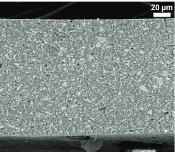
Figure 1 is microscope SEM image of a cryofractured filled sample edge, in the backscattered mode, with incident electrons accelerated at 10 kV. It shows the two kinds of fillers (the small brighter dots correspond to the iron(III) oxide) and their homogeneous dispersion in the polysiloxane matrix.
The glass transition temperature of both filled and neat materials were measured at −117 ± 1 °C, suggesting a low phenyl side groups content (from [10], the phenylmethylsi-loxane mass fraction was estimated to be approximately 10%).
2.2. Electron irradiations
Electron irradiations were performed under high vacuum in the SIRENE facility at ONERA. The procedure and dose calcul ations are detailed elsewhere [8] and summarised here. 150 µm thick elastomer films were irradiated using a 400 keV Van de Graaff electron gun along with a set of aluminium
Figure 1. SEM image of the edge of a cryofractured filled sample (10 kV, backscattered electrons) showing the high wt% and homogeneous dispersion of fillers.
scattering foils to uniformly expose the sample surface. The ionizing dose D expressed in Grays (1 Gy = 1 J kg−1) is
defined by (1). D d E x 1 d d ⎜ ⎟ ⎛ ⎝ ⎞ ⎠ = Φ (1)
where Φ is the particle fluence (in cm−2), d the material
den-sity, and dE/dx is the energy lost by an incident particle per unit length travelled in the material.
Ionizing doses up to 1.4 × 10⁶ Gy were achieved in less
than 12 h by means of high beam currents in the order of 10 nA cm−2. Samples irradiated in this way are uniformly aged (the dose deposited at the exposed face is less than two times lower than at the opposite face), and the doses mentioned throughout this manuscript are mean values corresponding to the dose in the middle of the film thickness.
2.3. Broadband dielectric spectroscopy
Broadband dielectric spectroscopy measurements were per-formed isothermally in the frequency range (10−2; 106 Hz)
on ~150 µm thick films placed between gold-plated stainless steel electrodes (diameter = 30 mm). Using a Novocontrol broadband dielectric spectroscopy (BDS) 4000 impedance analyser, sinusoidal voltages of varying frequency U∗(ω) were
applied to the sample while the intensity and phase shift of the current I∗(ω) were measured, allowing us to determine the
complex impedance Z∗(ω) of the sample.
The complex dielectric permittivity was calculated from the experimental impedance values as in (2).
″ ε ω ε ω ε ω ω ω = ′ − = ∗ ∗ C Z i 1 i 0 . ( ) ( ) ( ) ( ) (2)
The complex electrical conductivity was calculated by means of its definition (3), which directly links it to the com-plex dielectric permittivity.
″
σ∗ ( )ω =σ ω′( )+iσ ( )ω =iωε ε ω0 ∗( ). (3)
2.4. Surface potential decay
The surface potential decay (SPD) technique consists of depositing a finite electrostatic charge (by means of corona discharge or electron gun) at the surface of a dielectric sample, and then studying its isothermal decay dynamics. In this study, SPD measurements were performed at ONERA in a high vacuum (~10−6 mbar) specially designed enclosure. A STAIB
EG10 10 keV electron gun was used to charge the surface of ~150 µm-thick films and achieve initial potentials of ~ −4 kV. The surface potential was monitored by a TREK 341B non-contact vibrating Kelvin probe. A thermally-regulated sample holder (flow of liquid nitrogen and heating resistor) controlled temperature (−160; 150 °C).
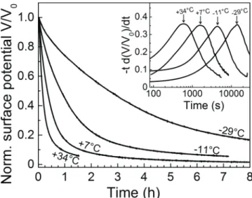
tdV/dt transformations were performed on the exper-imental SPDs. This mathematical transformation was first brought to the field of charge decay studies by Watson [11], and later generalised as a versatile tool for evidencing relaxa-tion and conducrelaxa-tion phenomena in disordered dielectrics [12].
When applied to a simple exponential decay function (such as V0e−t/τ), this transformation turns it into a peak centred on
the decay time constant τ, with an amplitude of V0/e. When
applied to stretched exponential decays (such as in figure 2), it also produces well defined peaks that allow the determina-tion of experimental decay time constants, as evidenced by the inset of figure 2.
By analogy with the ideal parallel plate capacitor, and if one considers that charge transport is the only phenomenon occurring during the potential decay, the DC electrical con-ductivity of the material can be determined as in (4).
( ) ( ) ( ) σ ε ε τ = ′ T T T DC 0 SPD (4) where ε0 is the vacuum permittivity, ε′(T) is the real part of the
relative permittivity (obtained from dielectric spectr oscopy measurements at 10−2 Hz), and τSPD is the exper imental
decay time constant obtained by SPD measurement and tdV/ dt transformation.
3. Results and discussion
In the ionizing dose range performed in this study, the cross-link densities of the materials were previously shown to be linearly increasing functions of absorbed ionizing dose [8], in agreement with Delides and Shepherd [13] who observed a linear increase of crosslink density up to 1.6 × 10⁶ Gy of
γ-rays in polydimethylsiloxane, followed by a sublinear dependence. In this section, the ionizing doses are therefore proportionally linked to the crosslink density of samples.
3.1. Effect of electron irradiation on electrical charge transport
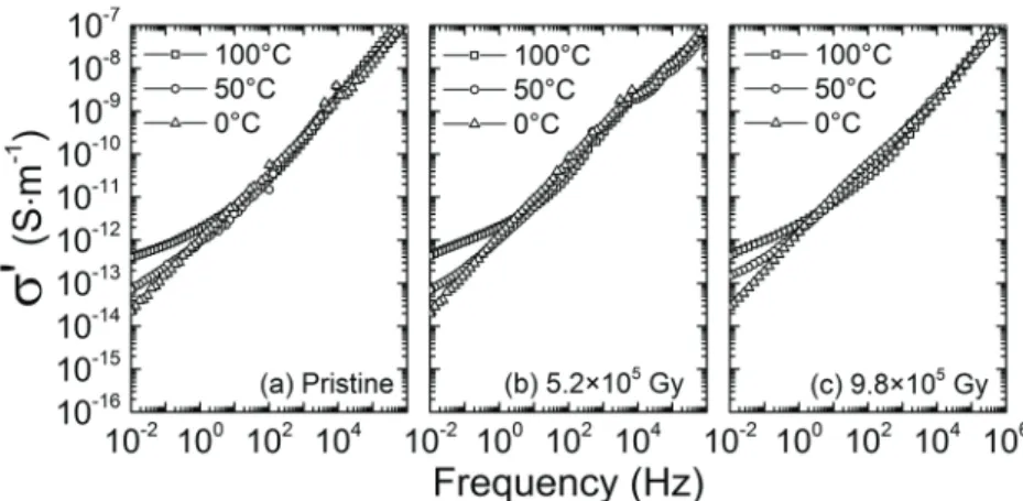
Conductivity spectra obtained by broadband dielectric spectr-oscopy on pristine and irradiated neat samples are represented in figure 3. They exhibit the typical behaviour of disordered
Figure 2. Isothermal surface potential decay curves for the pristine filled material at various temperatures, normalised to the initial potential V0. Inset: tdV/dt transformations of the SPD curves.
di electrics: a DC (direct current) plateau at low frequencies fol-lowed by a power law of frequency at higher frequencies. Pollak and Geballe first noticed such frequency power laws on a pure silicon crystal at low temperature [14]. Later, Jonscher [15] pro-posed to generalise it to all disordered dielectric mat erials under the name ‘universal dielectric relaxation response’ as in (5).
( )
σ ω′ =σDC+Aωs, 0< <s 1. (5) The DC plateaus allow straightforward determination of the DC electrical conductivity σDC(T ), which displays Arrhenius
dependence as in (6) with an activation energy of ~0.4 eV in the pristine case. This is in good agreement with the results of a previous paper [16]. T e E k T DC a B ( ) σ =σ∞ − (6)
where σ∞ is the pre-exponential factor, Ea is the activation
energy of charge transport, kB is the Boltzmann constant, and
T is the temperature.
By definition, the structure of disordered solids such as amorphous polymers lack periodicity which is a prerequisite for the band theory of charge transport. Following the early work of Mott [17], charge carriers hopping through localised states was progressively accepted as the main charge transport process in such solids, regardless of the majority of carrier being electrons or ions [18, 19], which are to date the only models able to predict the universal dielectric response [20]. The Arrhenius dependence of DC conductivity suggests a nearest-neighbour hopping mechanism (in contrast to Mott’s variable range hopping, which involves jumps over farther distances to exonerate from too high energy barriers, resulting in an e T T 11 4
( )
/ −dependence) [21]. The order of magnitude of the activation energy suggests an electron hopping mechanism rather than ionic transport, generally influenced by molecular mobility and with activation energies usually greater than 1 eV [22].
A decrease in σDC with increasing ionizing dose is
observed in figures 3(b) and (c), accompanied with an increase in measurement noise. However, the universal shape of the real component σ′( f ) of the complex electrical con-ductivity (as defined in (3)) is still observed in the spectra of irradiated samples, which suggests that the nature of the
transport mechanism did not change under the influence of ionizing radiations.
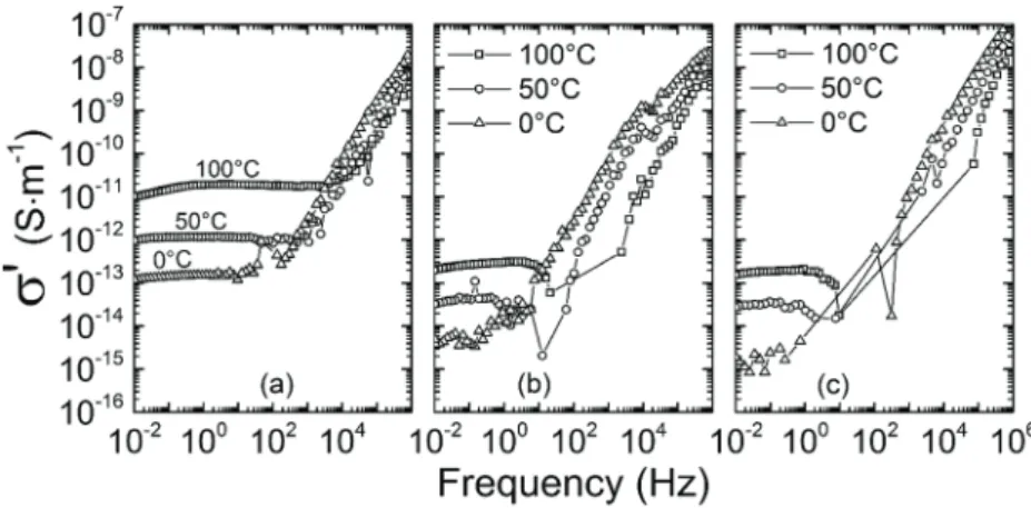
Conductivity spectra obtained by broadband dielectric spectr oscopy on pristine and irradiated filled samples are repre-sented in figure 4. As opposed to spectra of neat samples, no DC plateaus are observed at low frequencies, which is attributed [16] to Maxwell–Wagner–Sillars (MWS) polarisation [23]. Charge carriers are trapped around the inorganic silica and iron oxide fillers incorporated into the matrix, thus forming macrodi-poles which add frequency dependence to the low-frequency electrical response of the material. The fillers with large size distribution, especially silica fillers, result in a large distribu-tion of macrodipoles relaxadistribu-tion times, which are responsible for the disappearance of DC plateaus at low frequencies. Charge transport is influenced by MWS polarisation in the sense that conservative phenomena (charge trapping) are added up to the purely dissipative DC transport. This low-frequency behaviour was called low-frequency dispersion (LFD) by Jonscher [24].
Figures 4(b) and (c) show no significant evolution in the conductivity spectra of the filled material after electron irradi-ation. While DC conductivity of the polymer matrix decreases (as seen in figure 3), MWS polarisation still exists at the filler– matrix interfaces, and seems to dominate the low-frequency response of the filled samples regardless of the ionizing dose.
To avoid most MWS polarisation contributions to the trical response, isothermal SPD was performed. A DC elec-trical field was applied during SPD measurements, as opposed to AC fields applied in BDS. Figure 5 features an Arrhenius plot of DC conductivity measured by SPD on pristine and irra-diated, neat and filled samples.
With the minor exception of the pristine neat sample (Ñ) showing two slightly deviating points at low temperatures, all DC conductivities could be satisfactorily fitted with Arrhenius laws. The resulting Arrhenius fit parameters are reported in table 1 (neat samples) and table 2 (filled samples).
The decrease in conductivity of the neat samples upon irra-diation, already evidenced by BDS (see figure 3), is observed again with SPD. Moreover, the use of a DC applied field instead of the AC field employed in BDS reveals an even more pronounced decrease in the DC conductivity of the filled sam-ples. Tables 1 and 2 show that the activation energy of the filled material doubled after irradiation, while only slightly
Figure 3. Broadband dielectric spectroscopy real conductivity spectra for the neat material: (a) pristine, (b) irradiated at 5.2 × 10⁵ Gy, and
decreased with the neat material. The incorporation of silica and iron oxide fillers is therefore responsible for the signifi-cant discrepancies observed in the evolutions related to charge transport upon ionizing irradiation.
3.2. Filler influence on the evolution of ρDC and structure–
property relationships in light of electronic percolation theory
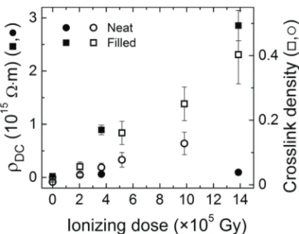
For both neat and filled materials, the electrical resistivity mea-sured by SPD at 30 °C, and the crosslink density determined by swelling tests (taken from [8]), are represented on the same ionizing dose scale in figure 6. The linear scale shows the dis-parity in the evolution of resistivity caused by the presence of fillers, which was less noticeable in the Arrhenius plot in figure 5. A similar disparity can be observed in the evo lution of crosslink density, which was attributed to an additional crosslinking process occurring at the filler–matrix interfaces in the filled material [8]. Similarities in the evolutions of resis-tivity and crosslink density highlighted in figure 6 most likely evidence a correlation between the electrical resistivity and chemical structure of this elastomer.
Miller and Abrahams [25] suggested that calculating the electrical conductivity of a dielectric material came down to calculating the conductivity of a random network of resistors. In this view, the electron or ion hopping rates between pairs of localised states (or traps) are associated with equivalent resistors. These hopping rates depend on the physicochemical structure of the material, as jumps across two sites will be easier when spatially and energetically close to each other. The randomness of the resistor network therefore stems from the extremely disordered nature of amorphous dielectrics. Ambegaokar et al [26] and Shklovskii and Efros [27] devel-oped percolation approaches to solve this problem, which assume charge transport occurs along a 1D ‘critical subnet-work’ consisting of the subset of resistors of least impedance that yet span the entire system: the percolation path. In this context, the net resistance of a sample is therefore dominated by the largest resistors within the percolation path, which act as bottlenecks [18]. According to Dyre [20, 28], the activation energy of the macroscopic DC conductivity corresponds to the largest activation energy met on the percolation path, that is, the energy barrier of the bottleneck.
The activation energies of σDC were determined as the slope
of linearly fits of the curves in figure 5. These activation ener-gies are displayed with respect to ionizing dose in figure 7. In the neat material, the activation energy of DC conductivity only slightly decreased after irradiation at 3.6 × 10⁵ Gy, as seen
Figure 4. Broadband dielectric spectroscopy real conductivity spectra for the filled material: (a) pristine, (b) irradiated at 5.2 × 10⁵ Gy, and
(c) irradiated at 9.8 × 10⁵ Gy.
Figure 5. Arrhenius plot of σDC as measured by SPD on irradiated
neat (open symbols Ñ, ◻, ∆) and filled (filled symbols •, ■, ▴)
samples. Corresponding values of temperature and σDC are
displayed on the upper x-axis and right-hand y-axis, respectively. Arrhenius fits of data are represented by dashed lines.
Table 1. Arrhenius fit parameters of σDC measured by SPD on a
pristine and two irradiated neat samples.
Ea (eV) σ∞ (S · m−1)
Pristine 0.41 ± 0.05 (1.0 ± 1.1) × 10−6 3.6 × 10⁵ Gy 0.32 ± 0.03 (2.9 ± 1.4) × 10−9
1.4 × 10⁶ Gy 0.33 ± 0.03 (3.4 ± 2.3) × 10−6
Table 2. Arrhenius fit parameters of σDC measured by SPD on a
pristine and two irradiated filled samples.
Ea (eV) σ∞ (S · m−1)
Pristine 0.33 ± 0.03 (1.5 ± 0.9) × 10−6
3.6 × 10⁵ Gy 0.61 ± 0.05 (1.9 ± 3.6) × 10−5
in figure 7 and table 1. It is believed that given the relatively spread out confidence interval associated with the pristine neat sample, the significance of this decrease is questionable. In the filled material, however, the activation energy of charge trans-port doubled after being exposed to a dose of 3.6 × 10⁵ Gy.
For a dose of 1.4 × 10⁶ Gy, no further evolution of the
activation energy was observed in neither the neat nor filled materials.
Interpretation of such discrepancy stems from the struc-tural evolution of materials upon irradiation. It was shown in a previous paper [8] that filler incorporation to this matrix resulted in an additional radiation-induced crosslinking mech-anism occurring through the formation of SiO4 covalent bonds
at filler–matrix interfaces, while crosslinking of the unfilled matrix mainly proceeded through the densification of SiO3
covalent bonds within the network.
In the framework of percolation theory, chemical bonds constitutive of the 3D polymer network can be associated with energy barriers that the electrons must overcome by means of thermally assisted hopping. Under the influence of an external electrical field, macroscopic drift currents flow across the sample through the percolation path, which is likely to be altered by chemical structure evolution following ionizing irradiation. In the neat samples, the small sensitivity of activa-tion energy to irradiaactiva-tion may be attributed to an invariance in the constitutive elements of the percolation path. In par-ticular, while the densification of SiO3 crosslinks in the
net-work reflects on the percolation path and implies an increase in electrical resistivity (simplistically, the percolation path can be seen as a set of resistors in series [29]), the highest constitu-tive barrier seems to have remained the same as in the pristine state. This suggests that SiO3 bonds were already present in
the percolation path of the pristine neat sample.
With filled samples on the other hand, the activation energy of conductivity showed high sensitivity to irradiation. Following the same interpretation scheme as with the neat material leads to the conclusion that a higher energy barrier has become constitutive of the percolation path as a result of irradiation. This change in the percolation path is believed to be discrete, triggered at a ‘threshold’ ionizing dose level
which could not be determined in this study due to the lack of experimental points (the threshold lies somewhere below 3.6 × 10⁵ Gy). Above the threshold dose, even though
fur-ther crosslinks densification is observed (as seen in figure 6
for instance), the highest constitutive barrier on the percola-tion path remains constant. In light of the crosslinking mech-anisms evidenced in the filled material, the new highest barrier is very likely to be associated with the SiO4 crosslinks formed
at filler–matrix interfaces. In the percolation paradigm, and by comparison with the evolution in the unfilled material, several conclusions can be drawn about these interfacial crosslinks. On one hand, they are associated with the highest energy barrier or trap in the material (~0.6 eV, which relates to the potential well an electron must overcome to move along the percolation path). On the other hand, the steep increase in acti-vation energy observed upon irradiation suggests they were left outside the percolation path due to their low density in the pristine state. This contrasts with those of matrix-related SiO3. Finally, the more pronounced decrease in electrical
conductivity observed in the filled samples is consistent with the percolation approach: the percolation path incorporates an increasing number of deep traps (SiO4), which results in
increasing its overall resistance.
3.3. Criticality of adhesive formulation for space applications
The decrease of intrinsic DC conductivity upon electron irra-diation is of prime importance when it comes to space appli-cations, particularly for surface dielectric materials. In the geostationary space environment, these materials will expe-rience dose levels similar to those performed in this study, though much less homogeneously spread over volume due to low-energy particles having higher fluxes. As noted in a previous study [8], five years is a very rough estimate of the time needed in geostationary orbit to reach 1.4 × 10⁶ Gy in
the middle of a 150 µm thick silicone film directly exposed to the geostationary electron environment. Near the exposed surface however, this time is greatly reduced (e.g. one year 20 µm below the surface) and it is safe to expect exposure to such ionizing doses during the operational lifetime of any sur-face material in the geostationary space environment.
Figure 7. Activation energy of σDC versus ionizing dose, for the
neat (Ñ) and filled (■) materials.
Figure 6. Evolution with respect to ionizing dose of DC electrical resistivity as measured by SPD (left-hand y-axis, filled symbols •,
■), and crosslink density determined by swelling tests (right-hand y-axis, open symbols Ñ, ◻, from [8]).
DC electrical conductivity is directly linked through (4) to the decay time constant of accumulated charges at the surface of a dielectric film. This time constant may be used to quantify the risk associated with triggering electrostatic discharges, which requires surface charge accumulation up to a few kV. Somewhat arbitrary time constant limits can be set and asso-ciated with a risk of electrostatic discharge. For instance, Dennison et al [30] suggested that this risk became critical when the time constant exceeds 24 h, which corresponds to the period of revolution in geostationary orbit, and was negligible when the time constant is lower than 1 h.
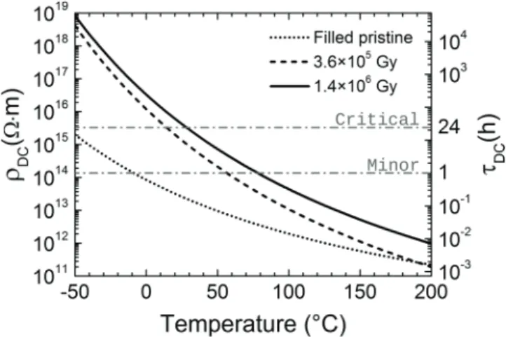
Electrical resistivity deduced from extrapolations of Arrhenius fits of conductivity (SPD data, figure 5) are repre-sented over the temperature range (−50; 200 °C) in figure 8
for the neat material, and in figure 9 for the filled material. Associated time constants and electrostatic discharge risk limits are also displayed. The extrapolated resistivity values in these figures should be looked upon as highlighting evolution trends rather than reliable values. Moreover, accurate electro-static discharge risk anticipation requires consideration of all phenomena balancing surface charging in space applications: namely, photoemission, secondary emission, and radiation-induced conductivity, which results in immediate enhance-ment of electron hopping due to the interaction of incident ionizing radiations with the material [31]. In particular, the latter is expected to play a major role in telecommunication applications due to the high fluxes of ionizing radiations on the geostationary orbit by raising DC conductivity possibly by several orders of magnitude.
Regarding the neat material, figure 8 shows that even though its resistivity increases with irradiation, the associated risk of electrostatic discharge remains below the critical limit over the majority of the temperature range. On the contrary, as seen in figure 9, the resistivity of the irradiated filled samples becomes critical with respect to electrostatic discharge risk below room temperature.
Because ground testing of electrical properties is very often performed at room temperature only, the fact that the
two pristine materials have similar DC electrical behaviours and associated electrostatic discharge risks in this temper-ature region could be misleading regarding their evolution with ionizing irradiation. The inorganic fillers incorporated into the polysiloxane matrix to provide specific functionali-ties (namely, higher mechanical modulus, lower coefficient of thermal expansion, colour, thixotropy) have unforeseen impacts on its electrical properties, leading to the idea that a compromise might exist between filler reinforcement and induced degradation of electrical properties.
4. Conclusions
This study aimed at analysing the influence of radiation ageing on the electrical conductivity of a filled silicone elastomer. An increase in electrical resistivity with respect to ionizing dose was observed in both the filled material and its isolated (unfilled) polysiloxane matrix, but this effect was much less pronounced in the latter.
A phenomenological parallel was drawn between the increase in resistivity and the increase in crosslink density evidenced in a previous paper, as these physical properties displayed similar filler-related discrepancies. In light of the electronic percolation theory, charge transport occurs by hopping over a percolation path consisting of electron traps (localised states) in series. The SiO3 (matrix) and SiO4 (filler–
matrix interfaces) crosslinks were associated with electron traps formed upon irradiation. The increase in resistivity of the matrix was therefore attributed to the densification of SiO3
crosslinks. Since they are constitutive of the polymer network (and thus already present prior to irradiation), no significant evolution in the activation energy of electrical conductivity was observed. On the other hand, it is believed that the char-acteristic percolation path of the pristine filled sample does not contain SiO4 crosslinks. However, the results of this study
suggest that immediately above a minimum ‘threshold dose’, the percolation path starts to include at least one SiO4 bond,
accounting for the steep increase in activation energy. Its
Figure 8. ρDC of neat irradiated samples versus temperature,
from the extrapolated Arrhenius laws of conductivity (figure 5). Associated time constant for charge decay is displayed in the right-hand y-axis. Horizontal dashed lines indicate arbitrary boundaries for electrostatic discharge risk (minor 1 h and critical 24 h).
Figure 9. ρDC of filled irradiated samples versus temperature,
from the extrapolated Arrhenius laws of conductivity (figure 5). Associated time constant for charge decay is displayed in the right-hand y-axis. Horizontal dashed lines indicate arbitrary boundaries for electrostatic discharge risk (minor 1 h and critical 24 h).
stabilisation at higher doses is coherent with the percolation approach: the number of SiO4 bottlenecks along the
percola-tion path is uncorrelated to their energetic height.
While the pristine filled and unfilled materials are very similar from an electrostatic discharge risk viewpoint, the filler-related additional crosslinking mechanism causes the electrical resistivity of the filled material to be much more sensitive to ageing. These findings put the choice of adhesive formulation for space applications into new perspective: not only must it provide the material with desired functionality, but it should also be checked through ground testing that it does not induce unexpected evolutions of other properties (such as electrical) during its operational lifetime.
References
[1] Garrett H B and Whittlesey A C 2000 Spacecraft charging, an update IEEE Trans. Plasma Sci. 28 2017–28
[2] Tafazoli M 2009 A study of on-orbit spacecraft failures
Acta Astronaut. 64 195–205
[3] Reimer L 1998 Scanning Electron Microscopy: Physics of
Image Formation and Microanalysis 2nd edn (Berlin:
Springer) pp 3–7
[4] Egerton R F 2012 Mechanisms of radiation damage in beam-sensitive specimens, for TEM accelerating voltages between 10 and 300 kV Microsc. Res. Tech. 75 1550–6
[5] Charlesby A 1960 Atomic Radiation and Polymers vol 1 (Amsterdam: Elsevier) p 182
[6] Charlesby A 1991 The effects of ionising radiation on polymers Irradiation Effects on Polymers ed D Clegg and A Collyer (Amsterdam: Elsevier) pp 39–78
[7] Shimada A, Sugimoto M, Kudoh H, Tamura K and Seguchi T 2014 Degradation mechanisms of silicone rubber (SiR) by accelerated ageing for cables of nuclear power plant
IEEE Trans. Dielectr. Electr. Insul. 21 16–23
[8] Roggero A, Dantras E, Paulmier T, Tonon C, Dagras S, Lewandowski S and Payan D 2016 Inorganic fillers influence on the radiation-induced ageing of a space-used silicone elastomer Polym. Degrad. Stab. 128 126–33
[9] Hill D J, Preston C M and Whittaker A K 2002 NMR study of the gamma radiolysis of poly(dimethyl siloxane) under vacuum at 303 K Polymer 43 1051–9
[10] Polmanteer K E 1981 Current perspectives on silicone rubber technology Rubber Chem. Technol. 54 1051–80
[11] Watson P K 1995 The transport and trapping of electrons in polymers IEEE Trans. Dielectr. Electr. Insul. 2 915–24
[12] Llovera P and Molinie P 2004 New methodology for surface potential decay measurements: application to study charge injection dynamics on polypropylene films IEEE Trans.
Dielectr. Electr. Insul. 11 1049–56
[13] Delides C G and Shepherd I W 1977 Dose effects in the crosslinking of irradiated polysiloxane Radiat. Phys. Chem.
10 379–85
[14] Pollak M and Geballe T H 1961 Low-frequency conductivity due to hopping processes in silicon Phys. Rev. 122 1742–53
[15] Jonscher A K 1977 The ‘universal’ dielectric response
Nature 267 673–9
[16] Roggero A, Dantras E, Paulmier T, Tonon C, Balcon N, Rejsek-Riba V, Dagras S and Payan D 2015 Electrical behaviour of a silicone elastomer under simulated space environment J. Phys. D: Appl. Phys. 48 135302
[17] Mott N F 1967 Electrons in disordered structures Adv. Phys.
16 49–144
[18] Dyre J C and Schrøder T B 2000 Universality of ac conduction in disordered solids Rev. Mod. Phys. 72 873–92
[19] Tessler N, Preezant Y, Rappaport N and Roichman Y 2009 Charge transport in disordered organic materials and its relevance to thin-film devices: a tutorial review Adv. Mater.
21 2741–61
[20] Dyre J C 1988 The random free-energy barrier model for ac conduction in disordered solids J. Appl. Phys.
64 2456–68
[21] Vissenberg G 1999 Opto-electronic properties of disordered organic semi-conductors PhD thesis Universitat Leiden [22] Raju G G 2003 Dielectrics in Electric Fields vol 19 (New
York: Dekker) p 355
[23] Maxwell J C 1891 A Treatise on Electricity and Magnetism (Oxford: Clarendon)
Wagner K W 1914 Erklärung der dielektrischen Nachwirkungsvorgänge auf Grund Maxwellscher Vorstellungen Arch. für Elektrotechnik 2 371–87
Sillars R W 1937 The properties of a dielectric containing semiconducting particles of various shapes Inst. Electr.
Eng.—Proc. Wirel. Sect. Inst. 12 139–55
[24] Jonscher A K 1999 Dielectric relaxation in solids J. Phys. D:
Appl. Phys. 32 R57–70
[25] Miller A and Abrahams E 1960 Impurity conduction at low concentrations Phys. Rev. 120 745–55
[26] Ambegaokar V, Halperin B I and Langer J S 1971 Hopping conductivity in disordered systems Phys. Rev. B 4 2612–20
[27] Shklovskiĭ B I and Éfros A L 1975 Percolation theory and conductivity of strongly inhomogeneous media Sov. Phys.
Usp. 18 845–62
[28] Dyre J C 1993 Universal low-temperature ac conductivity of macroscopically disordered nonmetals Phys. Rev. B
48 12511–26
[29] Shante V K S and Kirkpatrick S 1971 An introduction to percolation theory Adv. Phys. 20 325–57
[30] Dennison J R, Brunson J, Swaminathan P, Green N W and Frederickson A R 2006 Methods for high resistivity measurements related to spacecraft-charging IEEE Trans.
Plasma Sci. 34 2191–203
[31] Fowler J F 1959 Radiation-induced conductivity in the solid state, and some applications Phys. Med. Biol. 3 395