HAL Id: hal-01622593
https://hal.archives-ouvertes.fr/hal-01622593
Submitted on 31 Mar 2020
HAL is a multi-disciplinary open access
archive for the deposit and dissemination of sci-entific research documents, whether they are pub-lished or not. The documents may come from teaching and research institutions in France or abroad, or from public or private research centers.
L’archive ouverte pluridisciplinaire HAL, est destinée au dépôt et à la diffusion de documents scientifiques de niveau recherche, publiés ou non, émanant des établissements d’enseignement et de recherche français ou étrangers, des laboratoires publics ou privés.
interferometry for STI CMP
Sophia Bourzgui, Agnès Roussy, Jakey Blue, Gaëlle Georges, Emilie Faivre,
Karen Labory
To cite this version:
Sophia Bourzgui, Agnès Roussy, Jakey Blue, Gaëlle Georges, Emilie Faivre, et al.. Device pattern impact on optical endpoint detection by interferometry for STI CMP. International Conference on Planarization/CMP Technology, Oct 2017, Leuven, Belgium. �hal-01622593�
Device pattern impact on optical endpoint detection by
interferometry for STI CMP
S. Bourzgui 1,2,3, a, A. Roussy 1, J. Blue 1, G. Georges 2, E. Faivre 3, K. Labory 3, A. Allard 3 1Mines Saint-Etienne and LIMOS, UMR CNRS 6158, CMP Georges Charpak, F-13541
Gardanne, France
2Aix Marseille Univ, CNRS, Centrale Marseille, Institut Fresnel, Marseille, France 3STMicroelectronics, Rousset, France
E-mail: [email protected]
In this study, the focus is made on interferometry endpoint detection for Shallow Trench Isolation (STI) Chemical Mechanical Planarization (CMP) process done on the first platen of the tool for a three platen-polishing configuration. The interferometry principle is based on light interferences produced by thin transparent and semi-transparent layers. Thus the removed thickness can be correlated to the intensity measured over time. The optical signal received during the SiO2 removal is affected by patterned wafers and pattern type. For STI stack, parameters like Gap Fill SiO2 thickness, trench depth, pattern density and surface topology, could be involved in laser light diffraction and scattering. In some cases, these unwanted effects are stronger than the periodical signal of the removed SiO2 layer thus, preventing from endpoint algorithm usage.
A correlation analysis has been performed based on experimental data between memory product layouts parameters and the response of raw signal detection. It confirms that the more sizable the Electrically Erasable Programmable Read-Only Memory (E²PROM) coverage is, the weaker and noisier the signal is. However, our experiment also shows that regardless of the SiO2 thickness, a deeper trench will produce a more exploitable signal. In conclusion, perspectives for future experimentations are explored, in order to set up CMP optical endpoint detection by interferometry for a broader type of memory device patterns.
Keywords: Planarization, Chemical-mechanical Polishing, optical endpoint, interferometry, STI CMP, device pattern.
1. Introduction
Many in-situ process control systems using different methods (optical, thermal, friction electrochemical, acoustic) have been developed to monitor platen-by-platen polishing time [1]. One of the most relevant process control widely used for CMP is optical endpoint detection, with a monochromatic laser [2] [3] or, a white-light source for advanced nodes [4]. Optical endpoint detection shows good results in compensating for wafer-to-wafer pre-CMP process thickness variations and reducing post-CMP process thickness variations compared to a process control based on polishing by a fixed time.
In this paper, the research is centered on the endpoint detection by interferometry for STI CMP process. In fact, the polishing time of almost all technologies in the production line of STMicroelectronics Rousset site is monitored by optical endpoint detection, except for a single category of products: 512kbits and more E²PROM memory chips. For those E²PROM memory
systems, the signal is noisier and the amplitude is weaker compared to standard logic products (Fig. 1). The objective is to understand better the signal shape in function of input and process parameters. In the first phase, for sake of completeness, the interferometry principle is explained. Additionally, a list of factors, that can impact the periodical signal of SiO2 removal, is drawn
up. Secondly, the focus is made on memory products, to better experimentally understand the signal response. A design of experiments of 25 runs combined three factors: E²PROM size, SiO2 thickness, and depth trench. At last signal shapes correlations with the entry parameters
will be analyzed. The conclusions to these experiments will give directions of future researches.
Fig. 1: The three graphs show 5 unfiltered signals of a) a logic product , b) 32kbits E²PROM product and c) 512kbits E²PROM memory product, each curve representing a wafer The sinusoid corresponding to the SiO2 layer removed over
time is easily seen for a) and b). For the 512 kbits memory product, a noise with a period of about 5 seconds and high amplitude, prevents the detection of the SiO2 thickness sinusoid.
2. Endpoint detection by interferometry
Endpoint detection by interferometry uses the properties of light interference caused by thin transparent and semi-transparent layers. Light interferences are obtained because SiO2 layer
thickness is about hundred nanometers scale, which is smaller than the laser beam diameter and reflected beams are superposed. For two reflected beams (Fig 2), the intensity detected is the addition of the intensity of the reflected beams by each layer (I1 and I2) and an interference term function of I1, I2 and of the phase difference between the waves[5] written:
I1 2 2√ 1 ∗ 2 ∗ cos , (1)
Additionally, can be expressed as a function of the optical path difference between the two waves, related to the material thickness crossed by the incident light:
∗
∗ ∗ ∗ 2 ∗ ∗ ∗ cos 1, (2)
where 1 is the transmitted beam refraction angle. The refractive index of removed material has to be known at the laser wavelength . Thanks to the equations (1) and (2), the SiO2
thickness removal can be determined in function of the intensity detected over polishing time.
Fig. 2: a) depicts the interferometry principle for the simple case of two reflected beams on a SiO2 layer above a silicon
substrate. I is the incoming beam intensity from the laser source and it is both reflected on the semi-transparent material
surface and the bottom layer. As the two reflected beams come from the same source, they initially have the same phase at the origin, but a different phase after reflection, defined by the optical path difference . b) represents a side view of the
endpoint system located under the polishing platen.
For the CMP, many parameters disturb the sinusoidal signal corresponding to the SiO2 removed
that can be split in two categories: CMP process factors and product design factors. CMP process factors include, movements of the rotating platen, the rotating head and the head sweep (Fig. 2b). Moreover, slurry particles can scatter the incident beam that reduce the detected intensity. However, these polishing recipe parameters do not change between technologies: slurry flow, head pressure, head and platen velocity are equal. Under these conditions, the significant difference of signal detection between logic and memory products (Fig. 1) can only be explained by entry process parameters and pattern device type.
3. Wafer pattern for memory products at active step
The signal is detected at the center of the wafer through a window of 45mm and an acquisition time of a few milliseconds. On the first platen, only the SiO2 removal is monitored and the
objective is to leave about 100nm of SiO2 above the Si3N4 layer, to obtain an optimal polishing
process on platen 2. The signal detected is influenced by the following parameters:
• The Gap Fill SiO2 surface topology: it can cause the incident light to be reflected in random directions, thus rendering the outgoing signal weaker and noisier. This phenomenon can happen at the beginning of polishing until the process reaches the full SiO2 portion. The Gap Fill topology surface depends on trench depth and thickness.
Fig. 3: The pictures represent cross sections of the Gap Fill deposition before STI CMP by Scanning Electron Microscopy (SEM) in two zones: memory and logic areas. The logic area has an uneven topology and varying trench widths, while the memory area is flat and trench width and spacing remain constant.
• Gap Fill SiO2 thickness and the trench depth: with a larger SiO2 thickness, the signal
shifts to the right (Fig. 3a) and for a deeper trench, the signal amplitude decreases (Fig. 3b).
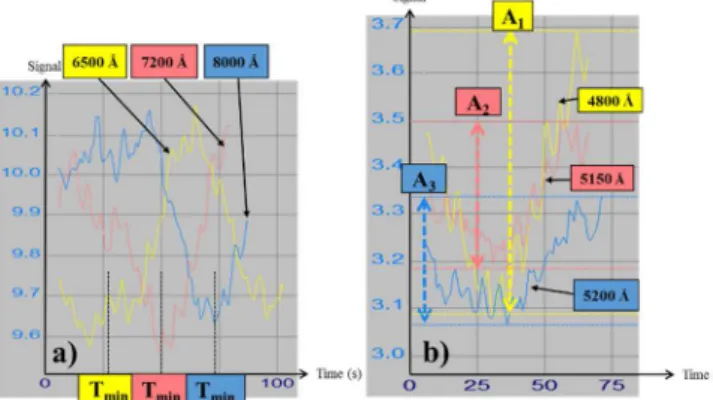
Fig. 4: On both graphs, each curve represents a wafer of the same product. a) depicts that with identical removal rates, pre-CMP process thickness variations cause the signal to shift over time. We can see that Tmin, the time at which the
signal intensity is the lowest, shifts to the right with thickness increases. In b) each wafer has a different trench depth: with the same removal rate, pre CMP process trench depth variation impact the signal amplitude An. In this case, A1 >
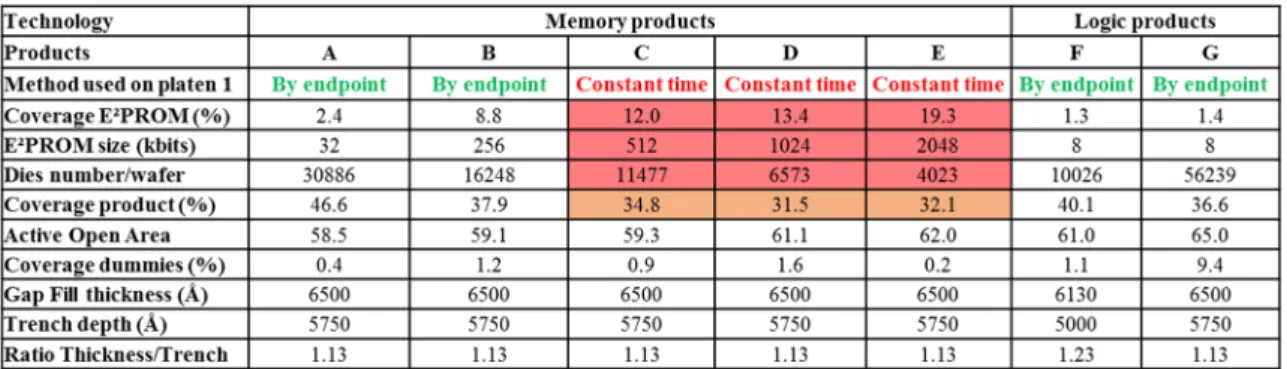
• The pattern type and the density: For some memory products, the use of an endpoint algorithm is already implemented in production. For these products (cf. Table 1) is that the E²PROM’s size is no larger than 256 Kbits and no larger than 9% of the chip’s surface. By comparing logic and memory products on Table 1, Gap Fill and trench depth do not highlight any relevant difference to explain the signal endpoint degradation issue. Likewise, the size of the Active Open Area for all products is within the specifications. The underlying factors causing a significant difference between products are the E²PROM size, the coverage of the E²PROM on the die, the number of dies per wafer: chip number decreases as the E²PROM size rises. The specificity of the E²PROM design is that the memory matrix is like a grid of SiO2 trenches that has a higher density
compared with logic zones.
Table 1 lists the key of certain memory and logic products. In the memory products section, we notice that the Gap Fill thickness and the trench depth are equal for all products.
In order to highlight the three points of this section, a Design Of Experiment (DOE) is set up with the following factors: Gap Fill SiO2 thickness, trench depth, and E²PROM size.
4. Experiments
The objective of this study is to analyze how the signal is impacted by the variation of incoming parameters for E²PROM products. Repeatability and reproducibility have not been tested in this experiment but will be assessed in at a later date time on exploitable signals. Considering a maximum of 25 wafers available, those parameters have been tested on three levels as follow:
Table 2: Input factors of the experiments to analyze their influence on the interferometric signal shape on platen 1
To study the E²PROM size influence, three memory products have been selected including one with a functional algorithm. The STI CMP process needs to respect a certain ratio between the trench depth and the SiO2 thickness, large enough to enable a good planarization and to avoid
a dishing effect in the non-dense zone of SiO2 [6]. This has driven the choice of the different
selected thicknesses for the experiment. Moreover, the trench’s depth factor studies the impact on amplitude variation, seen in Fig. 4b. Finally, the influence of surface topology has been tested, by combining different trench depths and SiO2 thicknesses.
In order to trace a signal long enough to configure an algorithm, wafers were polished with a fixed duration that including over-polishing. Furthermore, the data collection was made with no filters to be sure that the signal treatment is done properly on raw data. The goal is to have the same response during the algorithm development and real polishing conditions. To assess the Removal Rate (RR) of the tool, post measurement via off-line metrology ellipsometry tool
was made on a single wafer per E²PROM size, after polishing, in order to calculate the polishing time needed for platen 1.
5. Results
In our case of a limited number of 25 wafers, a D-Optimal experimental design has been selected. Considering the SiO2 thickness and trench depth factors, the values used to study the
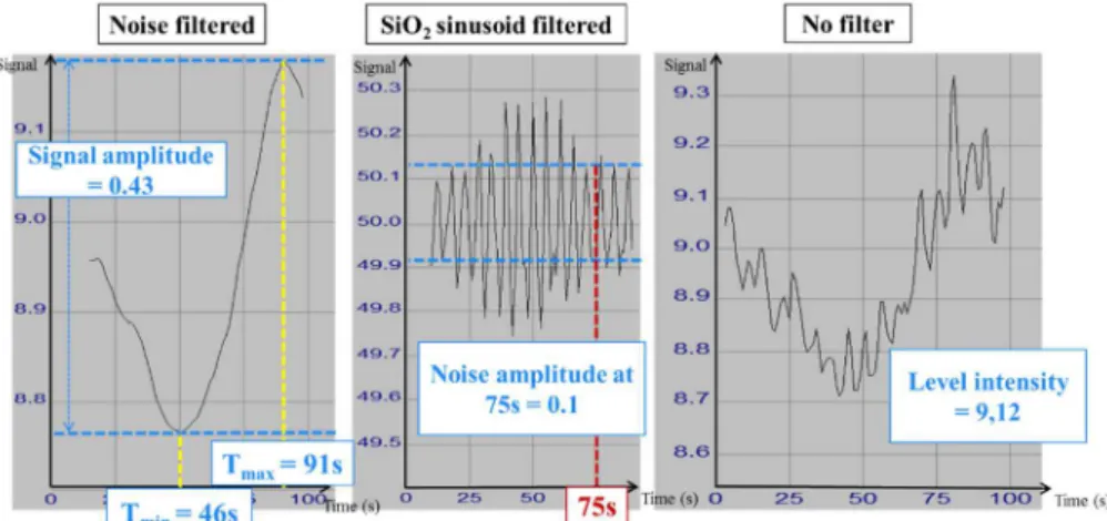
influence are the theoretical values. In fact, only a part of the wafers was measured in line for a concern of costs and availability of metrology tools. The interferometric signal response characteristic are defined as follow (Fig. 5): signal peak-to-peak amplitude, Tmin: the time at
which the signal intensity is the lowest and Tmax: the time at which the signal intensity is the
highest, periodical noise amplitude and signal level intensity. For a better precision of the responses concerning the signal characterization, specific filters were used for each response category.
Fig 5: Responses associated with the D-Optimal plan. Tmin, Tmax and the signal amplitude are determined from the SiO2
removal curve with noise filtering. On the contrary, the noise amplitude is given by filtering the SiO2 removal curve. Finally,
the intensity level is determined without any filter
The signal level intensity results, deduced by the value given by the software used for algorithm development, implied that the smaller the E²PROM size is, the higher the intensity. The signal peak-to-peak amplitude is characterized by filtering the periodical noise. The model shows that the trench depth and the SiO2 thickness have an impact on this parameter (Fig. 6). The signal
amplitude decreases for a trench depth value around 5750Å and increases at the edge of the domain for a 5350Å and 6150Å trench depth. The noise amplitude is defined by filtering each signal with a period to enhance filter of 5 seconds, corresponding to the average period of periodical noise for all curves. The filter erases the SiO2 layer sinusoid and only the noise is
visible. As expected, this parameter is influenced by E²PROM size, increasing with the biggest ones, but it is also influenced by the trench depth, the noise amplitude is the highest for the smaller one. Finally, the signal positioning over time is represented by Tmin and Tmax. On one
hand, the R² of Tmin response is weak (Table 3), which probably means that this parameter was
not correctly measured. On the other hand, the Tmax responses has a very good R² and R²adjusted
associated with a simple linear model which confirms that the SiO2 thickness is the most
Responses R² R²adjusted Influent factors Model
Level intensity 0.97 0.96 E²PROM / trench depth Quadratic Signal amplitude 0.896 0.86 Trench depth / SiO2 thickness Quadratic
Noise amplitude 0.82 0.78 E²PROM / trench depth Quadratic
Tmin 0.78 0.70 Trench depth / SiO2 thickness Square root
Tmax 0.97 0.965 E²PROM / trench depth / SiO2 thickness Linear
Table 3: Summary table of the experimental plan analysis. The models are calculated using the variance analysis method (ANOVA) taking into account the p-value terms less than 5%. The lower R² of the signal amplitude and Tmin responses can be
induced by the fact that five results are missing, because on certain curves the minimum amplitude is not distinguishable
Fig. 6: The response surfaces of a) the signal amplitude and b) the noise amplitude versus their influent factors.To determine the optima in terms of the value of SiO2 thickness and trench depth for the large E²PROMs, it is expected that the amplitude
should be as large as possible and the Noise amplitude to be as low as possible.
6. Conclusions and perspectives
In summary, how the memory product parameters affected the signal is studied in this paper. Our next step will be to classify the level of parameters and to define with which configuration the raw signal is exploitable for proper filtering. For example, and contrary to the experimental domain of depth trench seen in Fig. 4, these experiments show that for a deeper trench, the signal-to-noise ratio is improved and the signal shape is close to what it is expected: a clear distinction of the SiO2 sinusoid. Moreover, combined to the bigger Gap Fill, the sinusoid shape
presents a complete half period, compared with the other Gap Fill that could help set an endpoint window easily. In addition, with these two parameters, the thickness-trench ratio is respected. The second step will be, with available raw signals, to find a robust algorithm with efficient filters to support an endpoint. The essential element of an endpoint algorithm is that its repeatability and reproducibility are verified. Thus, algorithms have to be tested on more wafers to validate the endpoint detection robustness. In parallel, in order to make a deeper analysis on the optical phenomenon produced by the different positions of pattern wafers, a comparative study of the laser light behavior through different E²PROM size with different laser wavelengths will be set up. A better understanding of the observed signal noise origin for the biggest E²PROM sizes is expected.
7. References
[1] Hetherington, Dale L., and David J. Stein. In-line monitoring of chemical-mechanical polishing processes. Microelectronic Manufacturing'99. International Society for Optics and Photonics, 1999.
[2] Fang, S. J., et al. Control of dielectric chemical mechanical polishing (CMP) using an interferometry based endpoint sensor. Interconnect Technology Conference, 1998. Proceedings of the IEEE 1998 International. IEEE, 1998.
[3] Chan, David A., et al. Process control and monitoring with laser interferometry based endpoint detection in chemical mechanical planarization. Advanced Semiconductor Manufacturing Conference and Workshop, 1998. 1998 IEEE/SEMI. IEEE, 1998.
[4] Perrot, C., et al. STI CMP stop in Silicon Nitride controlled by FullVision TM endpoint. Planarization/CMP Technology (ICPT 2012), International Conference on. VDE, 2012.
[5] Hariharan, Parameswaran. Basics of interferometry. Academic Press, 2010.
[6] Li, Yuzhuo, ed. Microelectronic applications of chemical mechanical planarization. John Wiley & Sons, 2007.