Science Arts & Métiers (SAM)
is an open access repository that collects the work of Arts et Métiers Institute of
Technology researchers and makes it freely available over the web where possible.
This is an author-deposited version published in:
https://sam.ensam.eu
Handle ID: .
http://hdl.handle.net/10985/20018
To cite this version :
Erick Cardoso COSTA, Fabio Antonio XAVIER, Ricardo KNOBLAUCH, Cristiano BINDER, Walter
Lindolfo WEINGAERTNER - Effect of cutting parameters on surface integrity of monocrystalline
silicon sawn with an endless diamond wire saw - Solar Energy - Vol. 207, p.640-650 - 2020
Any correspondence concerning this service should be sent to the repository
Administrator :
archiveouverte@ensam.eu
E
ffect of cutting parameters on surface integrity of monocrystalline silicon
sawn with an endless diamond wire saw
Erick Cardoso Costa
a,⁎, Fabio Antonio Xavier
a, Ricardo Knoblauch
b, Cristiano Binder
c,
Walter Lindolfo Weingaertner
aaPrecision Engineering Laboratory (LMP), Mechanical Engineering Department, Universidade Federal de Santa Catarina, Florianopolis, SC, Brazil bMSMP Laboratory, Ecole Nationale Supérieure d’Arts et Métiers ParisTech, Aix-en-Provence 13671, France
cMaterials Laboratory (LabMat), Mechanical Engineering Department, Universidade Federal de Santa Catarina, Florianopolis, SC, Brazil
A R T I C L E I N F O
Keywords:
Diamond wire sawing Mono-Si
Surface integrity Brittle-ductile transition Wafering
A B S T R A C T
The cutting of silicon wafers using multi-diamond wire sawing is a critical stage in solar cell manufacturing due to brittleness of silicon. Improving the cutting process output requires an in-depth understanding of phenomena associated with cutting parameters. In order to investigate the influence of diamond wire sawing on surface integrity of monocrystalline silicon, a looped diamond wire was used and cutting parameters wire cutting speed, feed rate and wire tension were varied. The surface morphology was observed by scanning electron microscopy. Surface roughness Sawas measured with a non-contact profilometer. The brittle-ductile transition was identified
by presence of residual phases on sawn surface. A bevel-polishing method was employed to determine the microcrack depth. The results show that with higher feed rate the surface presents deeper and wider craters because of deeper penetration of diamond grain. On increasing wire cutting speed, there were more regions formed in ductile mode. The higher Savalues was observed on increasing both feed rate and wire tension, while
Sadecreased with an increase in wire cutting speed. The brittle mode was predominant with an increase in feed
rate, resulting in Si-I phase in regions formed in fragile mode. Material removal in ductile mode led to ap-pearance of a-Si phase at high wire cutting speed. No significant effect was observed on increasing wire tension. Subsurface microcracks mainly initiating from bottom of grooves generated by cutting mechanism. The most appropriate set of cutting parameters is the lowest feed rate and wire tension and highest wire cutting speed.
1. Introduction
Crystalline silicon is the main material used for manufacturing solar cells in the photovoltaic industry, with around 95% of the solar cells manufactured being based on this material (62% multi-crystalline si-licon and 33% monocrystalline sisi-licon). Consequently, the photovoltaic industry consumes approximately 90% of the crystalline silicon pro-duced globally. Crystalline silicon is favored over other semiconductor materials due to its abundance in the earth's crust, comprising ap-proximately 27% of the minerals present (Ozturk et al., 2018a; Yu et al., 2012). The semiconductor characteristics of crystalline silicon allows a high efficiency to be obtained in power generation.
In order to produce solar cells, crystalline silicon ingots are sawn into wafers with a thickness of 100–180 μm. Currently, the re-ciprocating multi-wire sawing (MWS) process is almost exclusively employed in the photovoltaic industry to cut hundreds, and even more
than one thousand, wafers from a single crystalline silicon ingot (Möller, 2014). The MWS processes are divided in multi-wire slurry sawing (MWSS) and multi-wire diamond wire sawing (MWDWS). MWSS is a free-abrasive machining method, referred to as the three-body wear mechanism. The cut is performed by a loose silicon carbide (SiC) abrasive dispersed in polyethylene glycol, which is supplied through nozzles over a wire web and carried by gravity to the wire in the sawing channel. MWDWS is performed through a two-body wear mechanism through the interaction of the bonded diamonds on the abrasive wire with the workpiece. MWDWS is widely applied for slicing brittle-hard materials, such as crystalline silicon, sapphire crystals, SiC, stones and optical glass (Gao et al., 2016; Wu, 2016).
Although both sawing processes are widely used in the industrial sector, MWDWS has some advantages over MWSS, including higher material removal rate, better surface quality and, if correctly used, lower machining cost per wafer (Chen et al., 2015; Liu et al., 2017a).
https://doi.org/10.1016/j.solener.2020.07.018
Received 28 April 2020; Received in revised form 27 June 2020; Accepted 6 July 2020
⁎Corresponding author at: Laboratório de Mecânica de Precisão (LMP), Departamento de Engenharia Mecânica– CTC, Universidade Federal de Santa Catarina,
Trindade, 88040-900 Florianópolis, SC, Brazil.
E-mail address:erick.cardoso.costa@posgrad.ufsc.br(E.C. Costa).
0038-092X/ © 2020 International Solar Energy Society. Published by Elsevier Ltd. All rights reserved.
However, the residual damage introduced by the sawing process, which includes surface roughness, phase transformation and microcracks, re-mains unavoidable and directly affects the main mechanical, optical and electronic properties of the crystalline silicon wafer (Liu et al., 2017a). Due to the manufacturing of thinner and larger silicon wafers, the damage to the surface integrity, mainly in the form of subsurface microcracks, decreases considerably the fracture strength of the sliced silicon wafer during the post-processing step (e.g., lapping and pol-ishing) as well as the lifespan of the solar module (Liu et al., 2017b; Ozturk et al., 2018b). This generates some concern given that MWDWS is a critical process in the solar cell production chain.
Strategies adopted to reduce the damage at the surface and sub-surface of monocrystalline silicon (mono-Si) wafers are associated with the applied cutting conditions, such as wire cutting speed (vc), feed rate
(vf) and wire tension (Twire), as well as the characteristics of the wire
(Kumar et al., 2016). Many researchers have been trying to understand the macro and micro-kinematics of the sawing process by means of mathematical models and experimental approaches. In the literature, experiments carried on MWDWS are not described in depth. Most re-searchers have focused on single-diamond wire sawing (DWS). Re-garding the surface integrity,Gao et al. (2016)investigated the
influ-ence of the cutting parameters (vc≤ 2 m/s; vf≤ 0.75 mm/min) and
different cutting fluids on the surface topography, surface roughness, subsurface damage, total thickness variation and bending of the sawn mono-Si. Liu et al. (2017a)evaluated the subsurface microcrack da-mage of mono-Si induced by DWS with different cutting parameters (vc≤ 1.5 m/s; vf≤ 0.75 mm/min). The authors formulated a
mathe-matical model to describe the microcrack formation based on fracture mechanics theory. Their experimental results validated the proposed model and showed that the depth of the microcracks is mainly influ-enced by both cutting parameters vcand vf.
Gao et al. (2019)carried out experiments to analyze the influence of the vf/vcratio on the brittle-ductile transition in the DWS of mono-Si.
On evaluating different cutting parameters (vf ≤ 0.75 mm/min;
vc≤ 2 m/s) they observed that the vf/vcratio has a significant
influ-ence on the material removal mechanism.Pala et al. (2020)introduced a method for the characterization of the surface morphology by image processing and they showed that both vcand vfinfluence the
percen-tage of ductility and fragility of the sawn surface of mono-Si. However, the authors carried out experiments employing kinematics similar to that of grinding and the material removal mechanism was not validated by the residual crystalline phase.Kayabasi et al. (2017)investigated the effects of variations in the wire cutting speed (vc≤ 4.5 m/s), feed rate
(vf≤ 2 mm/min) and oil/water emulsion ratio (100% and 30% oil) on
the surface roughness of sawn mono-Si wafers. An artificial neural network (ANN) was accommodated to predict the surface roughness parameter Rausing the data obtained from the DWS cutting
experi-ments. Ozturk et al. (2018b)used regression models to optimize the surface roughness (parameters Ra, Rqand Rz) of mono-Si specimens cut
with a diamond wire. They employed a wire cutting speed of vc≤ 4.5 m/s and feed rate of vf≤ 1 mm/min.
The aforementioned authors provided valuable results, but an ef-fective correlation between the cutting parameters and surface integrity of mono-Si wafers cut by DWS has not yet been established. Furthermore, the wire cutting speed of vc= 20 m/s is widely employed
in the wafering industry; however, few experiments have been con-ducted using a wire cutting speed close that value.Kumar et al. (2016)
analyzed the wear of diamond wires for a wire cutting speed of vc= 18 m/s.Knoblauch et al. (2018)carried out experiments using an
endless wire saw test rig to analyze the progression of wear in the diamond sawing of mono-Si, with a wire cutting speed of vc= 13.7 m/s
and constant feed force of Ff = 3.1 ± 0.6 N.Suzuki et al. (2017)
investigated the effect of the diamond grain size and number of sawing cycles on the surface roughness and subsurface damage using a wire cutting speed of vc= 29 m/s. However, although these authors applied
wire cutting speeds close to those used in industrial applications, the
influence of the cutting conditions on the surface integrity was not evaluated. A previous investigation revealed that there is a close re-lationship between the microcrack depth and surface roughness in terms of the parameter Rz, and that the surface and subsurface integrity
is strongly influenced by variations in the cutting parameters when si-licon is cut using the diamond wire sawing process (Costa et al., 2019). In order to contribute to the diamond wire sawing (DWS) tech-nology and better understanding the material removal phenomena in-volved in the sawing of mono-Si wafers, the effects of the main cutting parameters (vc, vfand Twire) on the surface integrity of sawn mono-Si
workpieces were investigated. This paper reports an experimental study on the characteristic of the brittle-ductile transition of the sawn surface of mono-Si and discusses the results considering the surface mor-phology, surface roughness, phase transformation and microcracks in the subsurface region. The present paper is an important study for the researches aiming directly increase the silicon wafer quality in photo-voltaic applications.
2. Experimental procedure
2.1. Experimental setup and design of experiments
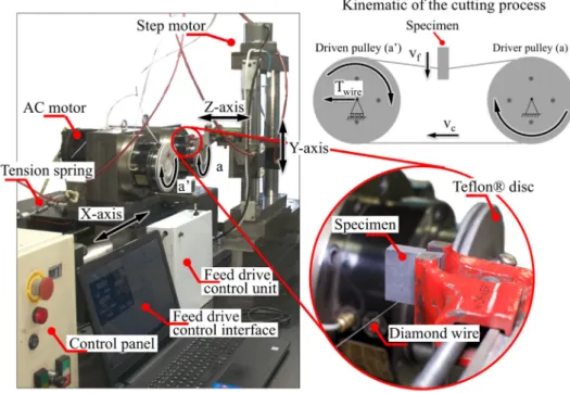
The experiments were carried out on the endless wire saw devel-oped byKnoblauch et al. (2017a), shown inFig. 1. In contrast to the industrial DWS machines, in this study a single-electroplated diamond wire in the shape of a loop was employed. Thus, instead of using a few thousand meters of wire for a multi-cut, single cuts were performed using only around a 1-meter segment of diamond wire. The ends of the industrial diamond wire segment were butt-welded on a welding device developed byKnoblauch et al. (2017b). After the loop shape had been obtained, the diamond wire was wrapped around two Teflon® discs and moved by the driven rotary axis with constant rotation to perform the cut with a constant wire cutting speed (vc).
The test rig slides and rotatory bearings (X, Y, Z, a and a′) are based on aerostatic slides/bearings, which ensure low friction on them (see
Fig. 1). This ensures that the applied forces are correspondingly applied in the cutting zone (no stick–slip effect on the input variables) and al-lows the cuts to be controlled with constant wire tension. The cut is performed by the endless diamond wire wrapped around two Teflon® pulleys, mounted on the front side of the two rotatory spindles. An electric AC motor, controlled by a frequency inverter, drives the main spindle. The maximum cutting speed of the wire is vc= 26 m/s. The
wire tension (Twire) is set by the air pressure on a pneumatic cylinder
and controlled by the deflection of a spiral spring. The vertical feed movement is driven by a step motor/ball bearing system. The minimum feed rate is vf = 0.08 mm/min and the value can be set using the
control interface. The width of the mono-Si specimen slices is manually set on the Z-axis by a micrometer adjustment screw.
The diamond wire used in this study is an industrial Ni electroplated diamond wire, manufactured by Norton Saint-Gobain Abrasives, with an outer diameter ØOD= 350 µm, wire core diameter of 250μm and
diamond grain size of 30–45 μm. The diamond grains are distributed randomly over the wire surface and bonded by a nickel (Ni) layer (Fig. 2).
Considering its widespread use in the manufacturing of solar cells, mono-Si was employed for this study, in the form of rectangular test specimens with dimensions of 25 mm × 50 mm × 7 mm (Fig. 3a). The specimens were sawn into slices (25 mm × 1 mm × 7 mm) with 1 mm thickness, parallel to the crystallographic plane (100), according to the Miller index (seeFig. 3b). The cutting direction in the kerf is normal to the crystallographic plane (010).
A full factorial design of experiments (DOE) was performed and experiments were carried out using the cutting parameters vcand vfat
three different levels (low, medium and high), and Twireat two levels
(low and high), as indicated inTable 1. Each experiment was performed three times.
For each single sawing experiment, a new (unworn) diamond wire was employed to minimize the effect of the wear of the diamond wire on the workpiece surface integrity. The cuts were performed dry. The sawn specimens were submitted to surface integrity analysis, based on the following techniques: surface morphology analysis by scanning electron microscopy (SEM), surface roughness analysis, micro-Raman spectroscopy and subsurface damage analysis (details are given in
Section 2.2).
A statistical evaluation was carried out to quantify the influence of the cutting parameters vc, vfand Twireon the surface integrity. Analysis
of variance (ANOVA), with a 95% confidence interval and confidence level ofα = 0.05, was performed to determine the effects of the factors, the divergence percentages and the p-values, as described by
Montgomery and Runger (2014).
2.2. Surface integrity analysis
2.2.1. Surface morphology
The surface morphology characteristics of the mono-Si specimens, sawn applying different cutting parameters, were determined by SEM (Hitachi TM-3030 microscope). The SEM micrographs allow the da-mage caused to the surface by the sawing process to be observed, which
provides information on the material removal mechanisms that act during the cutting process.
2.2.2. Surface roughness
The surface roughness of the sawn specimens is influenced by the characteristics of the diamond wire and the distribution of the diamond grains on the wire. Therefore, the surface roughness was measured using an optical non-contact profilometer (Zygo NewView 7300). Three-dimensional images of the surface topography were generated using the software MetroPro®, version 8.1.5. For each sawn specimen, images of three different regions, with an area of 1 mm2, were acquired
in order to obtain an average value for the measured surface roughness. The software MountainsMap Universal® 7.1 was used to process the measurement data, as recommended in ISO 16610–61, and the surface roughness parameter Sa(arithmetic average height) was extracted
ac-cording to ISO 25178–2. As a result, for the three specimens sawn under the same cutting conditions, an arithmetic mean value of Sawas
de-termined.
2.2.3. Raman spectroscopy
Raman spectroscopy was used to identify the presence of different crystalline phases on the sawn surface. The sawn specimens were Fig. 1. Endless wire saw test rig.
analyzed using a Renishaw® inVia micro-Raman microscope that op-erates with an Ar-laser (wavelength of 514.2 nm). The focal point of the laser was set on the sawn surface with an optical magnification lens (500x), and the Raman spectra were acquired through an accumulation of 10 s with three replicates in the bandwidth region of 200–700 cm−1
using the software Wire3.4®.
Based on considerations made byGao et al. (2019)regarding the influence of the r-ratio vf/vc(dimensionless) on the material removal
mechanism in DWS, four mono-Si specimens sawn with different r-ra-tios were analyzed. In each case, the analysis was performed twice and the two regions investigated showed evidence of (i) the brittle mode and (ii) the ductile mode of material removal. This step was carried out in order to confirm the presence of brittle material removal and the progression of ductile material removal in the region by detecting the residual crystalline phases on the sawn surface corresponding to each material removal mechanism.
2.2.4. Subsurface damage
Based on the ASTM F 950-02 standard, an embedding and bevel-polishing method was employed to analyze the depth of subsurface damage caused by the cutting of mono-Si specimens (seeFig. 4). The mono-Si specimens sawn by DWS were embedded in acrylic resin with a tilt angleα (°), after being ground and polished. The depth of the mi-crocrack damage observed on the polished surface was obtained under the bevel angleα, which permitted the geometric determination of the arithmetic mean depth of the microcracks for each specimen analyzed.
3. Results and discussion
3.1. Surface morphology
Figs. 5 and 6shows the SEM micrographs of the sawn surface of the mono-Si specimens cut with a wire tension of Twire = 20 N and
Twire= 30 N, respectively. The sawn surfaces are composed of parallel
and oriented grooves that follow the direction of the effective sawing movement, as also noted byBidiville et al. (2009) and Yu et al. (2012). Each SEM image shows areas with craters, microcracks and pitting, which are formed under the fragile (brittle) regime, and smooth areas characterized by the presence of parallel and oriented grooves, formed under the ductile regime. On comparing the nine cutting conditions evaluated for each Twire, it can be observed that the proportion of each
cutting regime varies with a variation in the cutting parameters (vcand
vf). This is in agreement with the results ofGao et al. (2019), although
the respective values of vcand vfwere much lower than the parameters
used in this study.
On applying a high vf, the material removal occurs predominately
through the fragile regime. Due to the penetration of the most pro-truded diamond grains into the mono-Si surface, corresponding to a high average undeformed chip thicknesses (hcu), on exceeding a critical
value (hcu,crit), plastic deformation gives way to microcrack formation
and propagation. A further increase in vf induces surface formation
predominantly with fragile fracture as the main material removal me-chanism. According toLiu et al. (2017b), an increase in vfleads to a
higher number of active diamond grains that effectively are assuming the cut, with material removed under the brittle regime, and this si-tuation progresses with increasing vf while maintaining vc and Twire
constant.
On the other hand, increasing vc, while maintaining the same
con-ditions described for the variation in vfand Twire, resulted in a reduction
in the microcracks and craters on the sawn surface. The diamond grains present different degrees of protrusion and their shapes vary, which leads to a difference in the stress state acting at point of grain/material contact. As a consequence, the sawn surface presents regions with evidence of mixed ductile and fragile modes, as seen in the SEM mi-crographs inFigs. 5 and 6. Considering afixed range of diamond grain protrusion and that all diamond grains are in contact with the surface of the mono-Si specimen, an increase in vcwould increase the engagement
frequency of the diamond grains on the mono-Si specimen along the sawing line, leading to a decrease in hcu. As a result, more kinematic
cutting edges will engage and contribute to the removal of ductile material, as reported byLiu et al. (2017b) and Chung and Le (2015). This change from brittle to ductile mode in the material removal me-chanism, resulting in surfaces with more regions that are free of frac-tures associated with the fragile mode.
All sawn surfaces obtained in these experiments exhibited both ductile and fragile material removal modes. The ductile regime was Fig. 3. Mono-Si test specimen: (a) dimensions and (b) crystallographic planes in detail.
Table 1
List of cutting parameters used in the cutting experiments.
Test vc(m/s) vf(mm/min) Twire(N)
1 10 20 20 2 10 30 20 3 10 40 20 4 15 20 20 5 15 30 20 6 15 40 20 7 20 20 20 8 20 30 20 9 20 40 20 10 10 20 30 11 10 30 30 12 10 40 30 13 15 20 30 14 15 30 30 15 15 40 30 16 20 20 30 17 20 30 30 18 20 40 30
dominant for the combination of highest vc and lowest vf. On
com-paring the results inFigs. 5 and 6, although the wire tension increases, the sawn surfaces under both wire tension conditions presented similar morphological characteristics, indicating a mixture of fragile and duc-tile modes as the material removal mechanism. However, the fragile behavior observed in the SEM micrographs inFig. 5is slightly more accentuated when the Twireis increased from 20 to 30 N, as can be seen
inFig. 6.
3.2. Surface roughness
The surface roughness is influenced by variations in vf, vcand Twire. Fig. 7shows the results for the variation in the arithmetic mean value for the surface roughness parameter Safor the mono-Si specimens sawn
under different cutting conditions. It can be observed that the mean value increases with an increase in vfand decreases with high vc, for
both Twirevalues. This can be explained by the combination of brittle/
ductile regimes during the chip formation. At high vfand low vcthe
sawn surface is formed by extensive fractured regions, observed in the form of craters (Jackson and Davim, 2011). According to Klocke (2008), fragile fractures can be attributed to an increase in the frictional force per grain and, consequently, higher hcudue to an increase in the
penetration of the diamond grains. Therefore, as described byBifano et al. (1991), the penetration depth has a significant influence on the
fragile fracture formation, resulting in the presence of more craters and pitting on the sawn surface.
The graphs inFig. 7show that the surface roughness parameter Sa
presented a slight reduction with an increase in vcfrom 10 to 20 m/s.
According toMarinescu et al. (2015), this behavior is associated with a reduction in hcuas a consequence of the higher engagement frequency
of the diamond grains on surface of the specimen. A lower penetration depth of the grains favors material removal in the ductile regime, re-ducing the surface roughness, since more damage-free regions are generated during the surface formation.
Higher Savalues were obtained for the highest vfand lowest vcfor
both wire tensions, as seen inFig. 7a and 7b. An increase in Twirecaused
Fig. 4. Schematic diagram of embedded and bevel-polished specimen.
an increase in the surface roughness with notably higher values of Sa.
An increase in the wire tension from 20 to 30 N reduced significantly the wire deflection during the cutting process. Considering the kine-matics of the cutting process shown schematically inFig. 8, it can be seen that in the initial stage (seeFig. 8a) there is no contact between the wire and the specimen, and the cutting wire movement remains per-pendicular to the feed rate (vf). With the feed movement of the
spe-cimen against the wire, a deflection effect was observed, as shown in
Fig. 8b. Although the chip removal mechanism of the diamond wire sawing is similar to that of the grinding process, the diamond wire is considered aflexible cutting tool. This characteristic generates a dis-placement of the free wire length in the form of a wire bow with an angle (Φ). In comparison to the initial stage (Stage 1), the diamond wire will then be in a new vertical position (Stage 2) caused by its deflection,
as shown inFig. 8c.
Applying a wire tension T2 > T1, for same condition of vcand vf,
result in an angleΦ2smaller than the wire bow angle (Φ1) generated
under a wire tension T1, as shown inFig. 8d. In the experiment was
observed that an increase in Twirefrom 20 to 30 N reduces the de
flec-tion effect and the wire bow angle (Φ) becomes smaller, resisting the force perpendicular to the cutting movement direction (component of feed force). As a results, there is a significant increase in the material removal rate due to the higher hcu, compared to that at Twire= 20 N. In
this regard, it can be stated that the higher material removal rate is the main factor that led to higher Savalues when the Twirewas varied from
20 to 30 N.
The behavior of the parameter Sa obtained from the surface
roughness measurements (seeFig. 7) are consistent with the surface Fig. 6. SEM micrographs showing the surface morphology of mono-Si specimens sawn under a wire tension of 30 N.
morphology of the mono-Si specimen sawn shown inFigs. 5 and 6. It can be observed that the sawn surfaces with more fragile fractures have the highest Savalues, whereas for the sawn mono-Si specimens with a
predominance of the ductile chip forming mechanism the variation in the arithmetic mean of the Savalues is significantly lower.
According to the ANOVA analysis, an increase in vcdecreased the
surface roughness parameter Saby up to 10.2% (p-value = 0.000894).
On the other hand, there was an increase in the Savalues on increasing
both cutting parameters vfand Twire. With an increase in vf, the value of
Saincreased by up to 15.6% (p-value = 0.000003). In the case of Twire,
an increase from 20 to 30 N resulted in an increase in the Savalues by
up to 34.3% (p-value = 0.000000). Based on the ANOVA results, it can be stated that variations in the cutting parameters vc, vfand Twirehad a
significant effect on the surface roughness of the mono-Si specimens, since the p-values remained at < 0.05 for all factors analyzed.
3.3. Raman spectroscopy
The SEM micrographs on the left side of Fig. 9show the regions analyzed by Raman spectroscopy for the specimens sawn applying different cutting conditions, considering the r-ratio (vf/vc). The image
in Fig. 9a shows a surface composed of extensive and deep craters, which indicates that there was a predominance of the fragile regime as the material removal mechanism. According toBifano et al. (1991), this characteristic suggests that hcuexceeded hcu,crit, which means that the
fracture resistance limit is reached before plastic deformation occurs, resulting in the material removal by fragile fracture. Therefore, the surface was formed through crack propagation resulting in the presence of craters on the sawn surface. The analysis of the phase transformation was based on the Raman spectra for the sawn surfaces, also shown in
Fig. 9. The spectra inFig. 9a show a single peak at 523 cm−1, corre-sponding to the cubic diamond phase structure (Si-I). According toWu and Melkote (2012), the Si-I phase is present in regions where the material removal mechanism was predominantly the fragile regime. Therefore, as the chip formation and removal was mainly by crack propagation, the pure crystal silicon (Si-I phase) becomes exposed.
The sawn surfaces shown inFig. 9b also exhibit a predominance of the fragile regime, evidenced by craters and a few damage-free spots.
The Raman spectra inFig. 9b show three new peaks at 349 cm−1(Si-XII phase), 433 cm−1 (Si-III phase), and 469 cm−1 (a-Si phase). The plasticity of the crystalline silicon have as primary mechanism the high-pressure phase transformation that cause brittle-ductile transition. The presence of these residual crystalline phases suggests that the Si-I phase underwent a phase transformation to the metallic phase Si-II due to the action of the grain/material contact pressure, which permits plastic deformation during chip formation. This is a result of the increase in vc
from 10 m/s to 15 m/s, which induces a lower hcuvalue due to the
highest engagement frequency of the diamond grain on the surface of the mono-Si. It can be stated that a value of vc= 15 m/s allows the
phase transformation of Si-I to metastable Si-II which can assume the crystalline and amorphous phases. The residual phases observed are formed by different unloading conditions: Si-XII and Si-III phases are attributed to a slow unloading rate and the a-Si phase is a result of a high unloading rate. These results can be attributed to the different levels of protrusion and shapes of the diamond grain, which lead to variations in the stress states underneath the grain/material contact point. Although there are different residual phases, the Si-XII, Si-III and a-Si phases occur due to the shear-induced phase transformation of the mono-Si during chip removal in the ductile regime.
The SEM micrographs inFig. 9c and 9d show the sawn surface of the mono-Si specimen obtained with r-ratios of 2.5 × 10⁻⁵and 1.6 × 10⁻⁵,
respectively. The characteristic predominance of a smooth surface can be observed with oriented, parallel and damage-free grooves, the so-called saw mark grooves. This suggests that on increasing vcand
de-creasing vfthe mono-Si cutting occurs predominantly in the ductile
regime, although the a few regions with craters are still presented, which indicates that part of the material was removed in the fragile regime due to different degrees of protrusion and shape of the diamond grains as well as lateral vibrations of the diamond wire.
The damage-free grooves correspond to the material removal me-chanism in the ductile regime, as can be observed by the appearance of a secondary phase of silicon due to the phase transformation phe-nomenon. This phase transformation from Si-I to Si-II with β-tin structure at high-pressure phase transformation results in the formation of an amorphous and metastable phase, which is a consequence of the ductile behavior of the mono-Si during plastic deformation. Under the Fig. 8. Influence of the wire tension on the kinematic of the cutting process.
ductile cutting conditions, it is possible to avoid microcrack initiation, since the mono-Si behaves as a ductile material during chip formation and removal. This is evidenced by the Raman spectra inFig. 9c and 9d, where the bandwidth of the amorphous phase (a-Si) has a peak at 475 cm−1. The presence of the a-Si phase is consistent with the ductile removal of mono-Si during the cutting, which is caused by grains that cut with hcubelow the critical value (hcu,crit) that produce a
microcut-ting as well as by grains that are only generates ploughing over the
workpiece surface.
Wang et al. (2020)reported that the phase transformation of the (100) mono-Si during high-speed scratching shows several residual phases as a consequence of the ductile mode of the material. The au-thors evidenced that at high-speed scratching between 10 m/s and 25 m/s there is an exponential increase in the intensity of the a-Si and Si-IV peaks on the Raman spectra, caused mainly by a higher unloading rate. Based on thisfinding, along with the results obtained during the Fig. 9. SEM micrographs and respective Raman spectra of sawn surfaces obtained with variations in the cutting parameters.
mono-Si cutting by diamond wire sawing experiments, it can be stated that vc= 10 m/s is the threshold for the phase transformation, and an
increase in vcgenerates a more intense phase transformation, which
leads to the amorphization of the silicon. In this regard, an increase in vc(10, 15 and 20 m/s) results in a sawn surface with a greater presence
of residual phases, which indicates the ductile removal mode for the mono-Si chips. This can be seen inFig. 9 (a, b, c and d), where the bandwidth and intensity of the a-Si phase observed on the Raman spectra increase progressively.
3.4. Subsurface damage
The SEM micrographs inFig. 10show the subsurface damage in the form of microcracks propagated from the surface to the subsurface. These microcracks are formed mainly due to the high brittleness and hardness of the mono-Si, as described by Lawn and Wilshaw (1975). During penetration of the diamond grains, fragile fracture takes place before plastic deformation occurs, leading to the nucleation and pro-pagation of microcracks into the subsurface of the mono-Si specimen.
According to the subsurface damage analysis reported inFig. 10, the measured average depth of the microcracks was within the expected range (between 2 and 20μm from the surface) (Möller, 2014). It can be observed that microcracks propagated mainly from the bottom of the grooves of the sawn surface. This is consistent with the restricted or-ientation of the diamond grains on the wire surface that introduces uniformly aligned microcracks along these periodic grooves. Moreover, many of the microcracks were median microcracks and slightly oblique, as also reported byXiao et al. (2019). This supports the hypothesis that lateral microcracks propagate to the surface and contribute to frag-mented chip formation.
With regard to the cutting parameters, an increase in vfresulted in
deeper subsurface microcracks. As seen inFig. 10a and 10b, increasing vffrom 20 to 40 mm/min resulted in an increase in the average depth of
the microcracks from 9.2 ( ± 1.1) to 11.9 ( ± 0.8) μm. According to
Gao et al. (2016), this increase in the microcrack depth occurs due to the high force per grain, which leads to a greater penetration depth of the kinematic cutting edges and, consequently, higher pressure on the workpiece material. This is in agreement with Klocke (2008), who stated that a higher force per grain results in deeper microcracks.
In contrast, when the increase of vcfrom 10 to 15 m/s (seeFig. 10b
and 10c), the average depth of the microcracks decreased from 11.9 ( ± 0.8) to 9.6 ( ± 1.0) μm. This reduction may be because an
increase in vc leads to a lower hcu value of the diamond grains and
reduces the nucleation and propagation of microcracks.
As seen in theFig. 10d, increasing vc(from 15 to 20 m/s) and
de-creasing vf(from 40 to 20 mm/min) caused a significant decrease in the
subsurface damage, which resulted in an average microcrack depth of 8.1 ( ± 0.9) μm. The microcrack depth analysis showed that for the cutting conditions investigated in this study, lower vfand higher vc
results in the lowest microcrack depth. This behavior can be attributed to a smaller undeformed chip thickness (hcu) and lower force per grain
of the diamond grains, leading to less damage to the surface integrity, as verified by the reduction in the microcrack depth.
The average values for the microcrack depth measured under dif-ferent cutting parameters are shown inFig. 11. It was found that the microcracks became deeper with an increase in vf, for the same vcand
for both wire tensions (Twire), because this increase allow the hcu,critfor
ductile-to-brittle mode transition to be exceeded. This generates deeper microcrack at the subsurface of the mono-Si specimen. The microcracks depth is associated with the morphological characteristics and increases when more craters are present on the sawn surface, exhibited by a high value for the surface roughness. This suggests that the surface mor-phology is close with subsurface damage. According to the ANOVA results, with a variation in vffrom 20 to 40 mm/min the microcrack
depth increased by up to 18% (p-value = 0.000169).
On increasing vc and keeping vfconstant, for both conditions of
Twire, there was a decrease in the microcrack depth. As previously
mentioned, the highest vc allows a reduction in the tangential and
normal loads of the active diamond grains. Under this condition, there is a lower force per grain, which decreases significantly the initiation and propagation of subsurface microcracks and, consequently, reduces the subsurface damage depth. The ANOVA analysis showed that an increase in vcresults in a reduction in the microcrack depth of up to
20% (p-value = 0.000003).
Regarding the cutting parameter Twire,this did not significantly
af-fect the average microcrack depth, as seen inFig. 11. In the ANOVA analysis, the p-value for the results obtained on increasing Twirefrom 20
to 30 N was 0.416201, which is higher thanα = 0.05. This behavior demonstrates that there is no difference between the average values obtained with a variation in the wire tension (Twire) under the
condi-tions analyzed in this study.
4. Conclusions
The cutting of mono-Si using the diamond wire sawing process was experimentally investigated. The experiments were performed applying different cutting parameters in order to evaluate their influence on the surface integrity of the cut mono-Si specimen. Aspects of the brittle-ductile transition phenomenon were discussed and supported by the surface morphology, surface roughness, identification of the material removal mechanism by residual crystalline phase on the sawn surface and depth of subsurface microcrack damage. Based on the experimental results obtained, it can be concluded that:
i. The sawn surface morphology exposed regions which had under-gone material removal in the fragile and ductile modes. The pre-dominant mechanism is dependent on the input cutting parameters. An increase in vfled to the formation of more fractures associated
with the fragile mode on the sawn surface. An increase in vcfavored
material removal in the ductile mode, reducing the surface damage. The sawn surfaces analyzed exhibited similar morphology for the two wire tensions (Twire) tested.
ii. An increase in vcresulted in a slight reduction in Sa, and increasing
vfpromoted the higher Savalues. This correlation between the vc
and vfparameters and the Savalue exhibited a similar behavior for
both Twirevalues. For Twire = 30 N, the Savalue increased
sig-nificantly when compared with the specimens sawn using Twire= 20 N. The results for the Saparameter also showed a
cor-relation with the surface morphology observed from the SEM ana-lysis.
iii. Raman spectra of the fractured regions exhibited the presence of the Si-I phase, which corresponds to the pure crystal phase of silicon. With a reduction in vfand an increase in vcthe sawn surface
pre-sented less fractures and more smooth areas with grooves aligned in the wire cutting direction. The grooves exhibited the metastable phases Si-XII and Si-III, as well as the a-Si phase, which indicates that the surface underwent phase transformation due to the grain/ silicon contact pressure. The cutting parameters vc and vf both
contributed significantly to the surface formation in the ductile re-gime, which was evidenced by the presence of the a-Si phase. The variation in Twirehad no significant effect on the phase
transfor-mation of the sawn surface.
iv. The microcracks in the subsurface originated mainly from the bottom of the machined grooves during the cut. An increase in vf
resulted in deeper microcracks, whereas increasing vcresulted in
lower microcrack depths. A decrease in vftogether with an increase
in vc led to lower subsurface microcracks damage. These results
were observed for both wire tensions (Twire) tested. The Twireno
present significate effect on the microcrack depth.
The experimental results for the surface integrity of mono-Si cut using the diamond wire sawing process under different cutting condi-tions showed that the cutting parameters have a significant influence on the sawn surface quality and the brittle-ductile transition of the mono-Si specimen. In future research the sawing forces could be measured to establish a correlation between the cutting parameters and the forma-tion of subsurface microcracks in the mono-Si specimen.
Declaration of Competing Interest
The authors declare that they have no known competingfinancial interests or personal relationships that could have appeared to in flu-ence the work reported in this paper.
Acknowledgements
The authors would like to thank the Coordination for the Improvement of Higher Education Personnel (CAPES) for thefinancial support; Saint-Gobain Abrasives for kindly providing the electroplated diamond wires and the Materials Laboratory (LabMat) at UFSC.
References
Bidiville, A., Wasmer, K., Kraft, R., Ballif, C., 2009. Diamond wire-sawn silicon wafers– from the lab to the cell production. In: 24th Eur. Photovolt. Sol. Energy Conf. Exhib. pp. 1400–1405.
Bifano, T.G., Dow, T.A., Scattergood, R.O., 1991. Ductile-regime grinding: a new tech-nology for machining brittle materials. J. Eng. Ind. 113, 184.https://doi.org/10. 1115/1.2899676.
Chen, K., Liu, Y., Wang, X., Zhang, L., Su, X., 2015. Novel texturing process for diamond-wire-sawn single-crystalline silicon solar cell. Sol. Energy Mater. Sol. Cells 133, 148–155.https://doi.org/10.1016/j.solmat.2014.11.016.
Chung, C., Le, V.N., 2015. Depth of cut per abrasive infixed diamond wire sawing. Int. J. Adv. Manuf. Technol. 80, 1337–1346.https://doi.org/10.1007/s00170-015-7089-z. Costa, E.C., dos Santos, C.P., Xavier, F.A., Weingaertner, W.L., 2019. Influence of
dia-mond wire sawing parameters on subsurface microcracks formation in mono-crystalline silicon wafer. In: ABCM (Ed.), 25th ABCM International Congress of Mechanical Engineering. ABCM, Uberlândia - MG, Brazil, pp. 1–8.https://doi.org/ 10.26678/abcm.cobem2019.cob2019-1574.
Gao, Y., Ge, P., Liu, T., 2016. Experiment study on electroplated diamond wire saw slicing single-crystal silicon. Mater. Sci. Semicond. Process. 56, 106–114.https://doi.org/ 10.1016/j.mssp.2016.08.003.
Gao, Y., Ge, P., Zhang, L., Bi, W., 2019. Material removal and surface generation me-chanisms in diamond wire sawing of silicon crystal. 104642. Mater. Sci. Semicond. Process. 103.https://doi.org/10.1016/j.mssp.2019.104642.
Jackson, M.J., Davim, J.P., 2011. Machining with Abrasives, Machining with Abrasives. Springer, US, Boston, MA https://doi.org/10.1007/978-1-4419-7302-3.
Kayabasi, E., Ozturk, S., Celik, E., Kurt, H., 2017. Determination of cutting parameters for silicon wafer with a Diamond Wire Saw using an artificial neural network. Sol.
Energy 149, 285–293.https://doi.org/10.1016/j.solener.2017.04.022.
Klocke, F., 2008. Manufacturing Process 2: Grinding, Honing, Lapping, RWTH. ed. Springer, Berlim - Germany.
Knoblauch, R., Boing, D., Weingaertner, W.L., Wegener, K., Kuster, F., Xavier, F.A., 2018. Investigation of the progressive wear of individual diamond grains in wire used to cut monocrystalline silicon. Wear 414–415, 50–58.https://doi.org/10.1016/j.wear. 2018.07.025.
Knoblauch, R., Costa, V.M.R.J., Weingaertner, W.L., Xavier, F.A., Wegener, K., Costa, J.V.M.R., Weingaertner, W.L., Xavier, F.A.A.F.A., Wegener, K., Da Silveira, C.A., Weingaertner, W.L., Xavier, F.A.A.F.A., Wegener, K., 2017a. Endless diamond wire saw for monocrystalline silicon cutting. In: 59th Ilmenau Scientific Colloquium. Technische Universität Ilmenau, Ilmenau, Germany, pp. 1–12.
Knoblauch, R., da Silveira, C.A., de Campos, J.E.S., Weingaertner, W.L., Xavier, F.A., Wegener, K., 2017b. Test rig for welding diamond wires into a loop. In: Proc. Fifth Intl. Conf. Adv. Civil Struct. Mech. Eng. - CSM 2017, pp. 37–41.https://doi.org/10. 15224/978-1-63248-132-0-38.
Kumar, A., Kaminski, S., Melkote, S.N., Arcona, C., 2016. Effect of wear of diamond wire on surface morphology, roughness and subsurface damage of silicon wafers. Wear 364–365, 163–168.https://doi.org/10.1016/j.wear.2016.07.009.
Lawn, B., Wilshaw, R., 1975. Indentation fracture: principles and applications. J. Mater. Sci. 10, 1049–1081.https://doi.org/10.1007/BF00823224.
Liu, T., Ge, P., Bi, W., Gao, Y., 2017a. Subsurface crack damage in silicon wafers induced by resin bonded diamond wire sawing. Mater. Sci. Semicond. Process. 57, 147–156.
https://doi.org/10.1016/j.mssp.2016.10.021.
Liu, T., Ge, P., Bi, W., Wang, P., 2017b. Fracture strength of silicon wafers sawn byfixed diamond wire saw. Sol. Energy 157, 427–433.https://doi.org/10.1016/j.solener. 2017.08.063.
Marinescu, I.D., Hitchiner, M.P., Uhlmann, E., Rowe, W.B., Inasaki, I., 2015. Handbook of Ceramics Grinding and Polishing, 1st ed, Handbook of Ceramics Grinding and Polishing. Elsevier, Waltham, USA. https://doi.org/10.1016/B978-1-4557-7858-4. 00011-X.
Möller, H.J., 2014. Wafer processing. In: Peter RudolphPeter Rudolph (Ed.), Handbook of
Crystal Growth: Bulk Crystal Growth. Elsevier B.V., Schönefeld - Germany, pp. 715–755 https://doi.org/10.1016/B978-0-444-63303-3.00018-3.
Montgomery, D.C., Runger, G.C., 2014. Applied Statistics and Probalisty for Engineers, 6th ed. John Wiley & Sons Inc, New York, USA.
Ozturk, S., Aydin, L., Kucukdogan, N., Celik, E., 2018a. Optimization of lapping processes of silicon wafer for photovoltaic applications. Sol. Energy 164, 1–11.https://doi.org/ 10.1016/j.solener.2018.02.039.
Ozturk, S., Aydin, L., Celik, E., 2018b. A comprehensive study on slicing processes op-timization of silicon ingot for photovoltaic applications. Sol. Energy 161, 109–124.
https://doi.org/10.1016/j.solener.2017.12.040.
Pala, U., Kuster, F., Wegener, K., 2020. Characterization of electroplated diamond wires and the resulting workpiece quality in silicon sawing. J. Mater. Process. Technol. 276, 1–9.https://doi.org/10.1016/j.jmatprotec.2019.116390.
Suzuki, T., Nishino, Y., Yan, J., 2017. Mechanisms of material removal and subsurface damage infixed-abrasive diamond wire slicing of single-crystalline silicon. Precis. Eng. 50, 32–43.https://doi.org/10.1016/j.precisioneng.2017.04.011.
Wang, B., Melkote, S.N., Saraogi, S., Wang, P., 2020. Effect of scratching speed on phase transformations in high-speed scratching of monocrystalline silicon. Mater. Sci. Eng. A 772, 138836.https://doi.org/10.1016/j.msea.2019.138836.
Wu, H., 2016. Wire sawing technology: A state-of-the-art review. Precis. Eng. 43, 1–9.
https://doi.org/10.1016/j.precisioneng.2015.08.008.
Wu, H., Melkote, S.N., 2012. Effect of crystallographic orientation on ductile scribing of crystalline silicon: Role of phase transformation and slip. Mater. Sci. Eng. A 549, 200–205.https://doi.org/10.1016/j.msea.2012.04.034.
Xiao, H., Wang, H., Yu, N., Liang, R., Tong, Z., Chen, Z., Wang, J., 2019. Evaluation of fixed abrasive diamond wire sawing induced subsurface damage of solar silicon wafers. J. Mater. Process. Technol. 273.https://doi.org/10.1016/j.jmatprotec.2019. 116267.
Yu, X., Wang, P., Li, X., Yang, D., 2012. Thin Czochralski silicon solar cells based on diamond wire sawing technology. Sol. Energy Mater. Sol. Cells 98, 337–342.https:// doi.org/10.1016/j.solmat.2011.11.028.