THESIS PRESENTED TO
ECOLE DE TECHNOLOGIE SUPERIEURE
IN PARTIAL FULFILLMENT OF THE REQUIREMENTS FOR
A MASTER'S DEGREE IN ELECTRICAL ENGINEERING
M.Eng.
BY
Roger EL-KAFROUNI
ENHANCEMENT AND VALIDATION OF A TEST TECHNIQUE FOR INTEGRATED
CIRCUITS
MONTREAL, MAY 10, 2010
1 Copyright 2010 reserved by Roger El-KafrouniBOARD O F EXAMINER S
THIS THESIS HAS BEEN EVALUATED BY THE FOLLOWING BOARD OF EXAMINERS:
M. Claude Thibeault, Thesis Supervisor
Departement de genie electrique a I'Ecole de technologic superieure
M. Ghyslain Gagnon, President of the Board of Examiners
Departement de genie electrique a I'Ecole de technologic superieure
M. Christopher Fuhrman, Member of the Board of Examiners
Departement de genie logiciel et des TI a I'Ecole de technologic superieure
THIS THESIS HAS BEEN PRESENTED AND DEFENDED BEFORE A BOARD OF EXAMINERS AND PUBLIC
April 9, 2010
Je tiens tout d'abord a exprimer ma reconnaissance envers mon directeur de maitrise et professeur titulaire, Dr. Claude Thibeault, pour son appui et sa confiance envers moi durant mon projet de recherche. Sa methode pedagogique etait enrichissante et a rendu mon projet de plus en plus interessant.
Je remercie aussi les etudiants du LACIME dont I'aide, le dynamisme et le travail remarquable ont contribue a creer une ambiance de travail cooperative et chaleureuse.
Je remercie mes parents et mes deux freres Michel et Paul, qui m'ont donne un support infmi, beaucoup de passion et d'espoir pour arriver a completer ma maitrise.
ACKNOWLEDGEMENTS
First and foremost, I wish to express my sincere appreciation and gratitude to my supervisor. Dr. Claude Thibeault, for his guidance and encouragement during my master's work.
I would like to thank the graduate students of LACIME; they have created a great cooperative and pleasant working environment.
I would like to dedicate this work to my parents and my brothers Michel and Paul. Their support, encouragement and understanding have been monumental during the course of my education. Without them, I doubt I would have been successful in my academic work.
AMELIORATION E T VALIDATION D'UN E TECHNIQUE D E TEST POU R CIRCUITS INTEGRE S
Roger EL-KAFROUNI RESUME
Ce memoire s'interesse a une approche de test recemment developpee a I'ETS. Cette approche, appelee methode de test dc delai sans capture (Capture-less Delay Testing, CDT), a ete proposee comme technique complementaire aux approches plus traditionnelles de test visant a s'assurer que les circuits integres fonctionnent a la frequence prevue, afm d'ameliorer la couverture de test de ce type de test. CDT utilise entre autres des capteurs permettant de detecter la presence de transitions a des endroits strategiques.
L'objectif de ce projet est d'ameliorer certains aspects de cette nouvelle approche. Dans un premier temps, nous allons analyser la distribution de delai des noeuds non couverts par les methodes traditionnelles de test, afin de developper la meilleure maniere de deployer les capteurs CDT. Nous presentons I'ensemble d'outils, utilisant le langage Perl, developpe a cette fin. Les resultats obtenus confirment que les chemins passant par les noeuds non couverts sont plus longs que ceux qui passent par les noeuds couverts. La difference entre les deux types de chemins represente plus de 20% de la periode d'horloge si Ton considere les delais des chemins les plus courts.
Dans un deuxieme temps, nous proposons un algorithme entierement automatise qui permet, pendant les premieres etapes du processus de generation automatise des vecteurs de test: 1) d'identifier les noeuds non couverts, 2) d'identifier les emplacements des senseurs CDT sur les entrees des bascules afin d'ameliorer la couverture de test, et 3) de minimiser le nombre de senseurs selon le besoin. Nos resultats indiquent que lorsque nous appliquons CDT en complement aux methodes transitionnelles basees sur le modele de pannes de type transition nous pouvons augmenter la couverture de test de pres de 5%. De plus, ralgorithme de minimisation du nombre de senseurs de CDT permet de reduire dc plus de 85% le nombre de ces senseurs avec une perte de couverture minimale, en moyenne de 1.6%.
Mots cles: circuits integres analogiques, generateur algorithmique de sequence de test, methode de test de delai sans capture, methode de test pour circuits integres.
Roger EL-KAFROUNI ABSTRACT
This thesis focuses on a scan-based delay testing technique that was recently developed at ETS. This new approach, called Captureless Delay Testing (CDT), has been proposed as a technique that complements traditional methods of test, ensuring the integrated circuits will function at their proposed clock speed, further improving the test coverage of the particular type of test. Furthermore, CDT incorporates the use of sensors enabling the detection of the presence of transitions at strategic locations.
The purpose of this project is to improve on certain aspects of this novel technique. At first, we analyze the delay distribution of the non-covered nodes by traditional methods of test, in order to develop the best way possible of placement of the CDT sensors. We present, using Perl Language, the ensemble of tools developed for this purpose. The end results obtained confirm that the paths that pass through the non-covered nodes are longer than those that traverse the covered ones. The difference between the two types of paths exceeds 20%) of the clock period when considering the shorter path delay values.
Secondly, we propose a fially automated algorithm that enables, at the earliest stages of the test vectors generation process: 1) the identification of the non-covered nodes, 2) the identification of the placements of the CDT sensors at the inputs of the flip-flops for further improvement of the test coverage, and 3) the minimization of the number of sensors with regards to requirements. Our results indicate that when we apply CDT on top of transition-based fault model we can improve the test coverage by 5%. Moreover, the algorithm of CDT sensors minimization allows a reduction of more than 85% the number of those sensors with a minimal test coverage loss, on average of 1.6%.
Keywords: analogue circuits, automatic test pattern generation, captureless delay testing, integrated circuit testing, low cost testing, scan-based test technique.
TABLE OF CONTENT S Page CHAPTER 1 INTRODUCTION 1 1.1 Motivations 1 1.2 Thesis Outline 3 1.3 Contribution 4 CHAPTER 2 MANUFACTURING DEFECTS AND DETECTION
MECHANISM 5
2.1 Introduction 5 2.2 IC catastrophic defects 6
2.2.1 IC catastrophic defects detection 7
2.3 IC parametric defects 8 2.3.1 Resistive vias 8 2.3.2 Metal mousebites 9 2.3.3 Metal Slivers 11 2.4 Parametric failures due to defects 11
2.5 Parametric timing failure due to process variation 12
2.6 IC delay defects detection 12
2.7 Summary 13 CHAPTER 3 EXISTING DELAY TESTING TECHNIQUES 14
3.1 Introduction 14 3.2 Functional testing 14
3.3 LBIST 15 3.4 Scan-based testing 15
3.4.1 Launch on shift (LOS) 17 3.4.2 Launch on capture (LOC) 18
3.5 Delay fault models 19 3.5.1 Path delay model 19 3.5.2 Transient fault model 20 3.6 Current DFT techniques limitations 20
3.6.1 Small delay defect 21
3.6.2 Testers limitafions 21
3.7 Conclusion 21 CHAPTER 4 CDT (CAPTURE-LESS DELAY TESTING) 23
4.1 Introduction 23 4.2 CDT Overview 23 4.3 CDT ftinctionahty 24 4.3.1 Implementation of CDT sensor 25 4.3.2 CTVC operation 27 4.3.3 Dynamic compensafion 28
4.3.4 CTVC 1st stage: Low Gain AmpHfication 29 4.3.5 CTVC 2nd stage: Differential Amplification 30
4.3.6 CTVC Buffering Stage 30 4.3.7 Delay measurement stage 31 4.4 Advantages of CDTP (Capture-less Delay Testing Patterns) 32
4.5 Conclusion 33 CHAPTER 5 TIMING BASED DELAY DISTRIBUTIONS OF TRANSITION
UNDETECTED FAULTS MODEL 34
5.1 Introduction 34 5.2 Scan based structural test techniques 34
5.3 ATPG methodology 35 5.4 Simulated implementation steps 37
5.5 Simulated results 37 5.5.1 Minimum path delay distribution of non-covered faults 37
5.5.2 Maximum path delay distribution of non-covered faults 38 5.5.3 Minimum path delay distribution of covered faults 39 5.5.4 Maximum path delay distribufion of covered faults 40 5.5.5 Comparing delay distribution of non-covered & covered faults 41
5.6 Conclusion 42 CHAPTER 6 ANALYSIS OF DELAY TEST EFFECTIVENESS WITH CDT
ON TOP OF LOC 43
6.1 Introduction 43 6.2 Capture-less Delay Testing CDT 44
6.3 Experiments CDT on Top-off LOC technique 44
6.3.1 Evaluation Framework 45
6.4 Contribution 46 6.4.1 Algorithm general steps 46
6.5 Algorithm implementafion 48 6.5.1 Implementafion steps 48 6.6 Running CDT on top of LOC patterns on muUiple ITC99 benchmarks 50
6.6.1 Proposed complementary ATPG process 50 6.6.2 Applying CDT random patterns on Un-detected faults 50
6.6.3 Un-optimized CDT sensors count coverage 51 6.6.4 Optimized CDT sensors count coverage 51 6.6.5 Summary of obtained test coverage results on selected ITC 99
benchmarks 52 6.6.6 Validating the obtained test coverage with the optimized list of sensors 54
6.7 Conclusion 54 CONCLUSION 56 ANNEX I LOGIC BUILT-IN SELF TEST BIST 59
VIII
ANNEX III PATH DELAY DISTRIBUTION PERL SCRIPTS 67
ANNEX IV CDT SENSOR PLACEMENT AND OPTIMIZATION PERL
SCRIPTS 79
BIBLIOGRAPHY 90
Table 2.1 Table 5.1 Table 6.1 Table 6.2 Table 6.3 Table 6.4 Table 6.5
Stuck-at truth table of a 2 input AND gate 8 Minimum, mean & maximum values of umin-pd(i), cmin-pd(j),
umax-pd(i), cmax-pd(j) expressed as a percentage of the clock period (T) 41
LOC test coverage results of ITC benchmarks 50 Un-optimized SS- random patterns test coverage results 51
Optimized SS-random patterns fault coverage results 52 Summary of simulated ITC 99 benchmark test coverage 53 A compromise of Test coverage with minimal CDT sensors use 54
LISTE DES FIGURE S
Page
Figure 2.1 Global and local manufacturing defects 6
Figure 2.2 Logic AND gate 7 Figure 2.3 Resistive vias 9 Figure 2.4 Defect-free and a defective interconnect 9
Figure 2.5 Zoom-in defective interconnect 9 Figure 2.6 Normal Metal line and one with mousebite 10
Figure 2.7 Voided metal resistance (mQ) versus percent 10
Figure 3.1 Shifting patterns in scan chains 16 Figure 3.2 Capturing the response of the combinatorial logic 16
Figure 3.3 Launch on shift transition delay fault pattern generation 17 Figure 3.4 Launch on capture transition delay fault pattern generation 18
Figure 4.1 Scan based CDT architecture 25 Figure 4.2 CDT sensor implementation: intrinsic (blue), extrinsic (burgundy), 26
Figure 4.3 Current to voltage conversion CTVC block 27
Figure 4.4 Dynamic compensation on Vddl3c 28 Figure 4.5 (a)Low gain amphfier, (b) and a differential amplifier 29
Figure 4.6 CDT Timing Diagram 31 Figure 5.1 Path delay distribution extraction flow 36
Figure 5.2 Minimum path delay distribufion of non-covered faults 38 Figure 5.3 Maximum path delay distribufion of non-covered faults 39 Figure 5.4 Minimum path delay distribution of covered faults 40 Figure 5.5 Maximum path delay distribufion of covered faults 41
Figure 6.1 Benchmark test coverage evaluation 45 Figure 6.2 CDT sensor aflocation, placement and optimization flow 47
Figure 6.3 CDT sensor allocation, placement and optimization implementation
LIST OF ABREVIATION S ASIC Application-specific integrated circuit
ATPG Automatic test pattern generation ATE Automatic test equipment
CDT Capture-less delay testing
CDTP Capture-less delay tesfing pattern CMP Chemical mechanical polishing CTVC Current to voltage conversion block CUT Circuit under test
CVP Current voltage pulse
DC Dynamic compensation block DFT Design for testability
DM Delay measurement block DVP Data voltage pulse
LB 1ST Logic built-in self test
LFSR Linear feedback shift register LOC Launch from capture
LOS Launch from last shift SOC System on chip
SSS Sensors switching at the same time STA Static timing analyzer
INTRODUCTION 1.1 Motivation s
"The success of the semiconductor industry has been due in large part to its ability to continuously increase the complexity, and therefore the processing power, of integrated circuits" [Nanowerk Spotlight]. Moore's law predicts that the number of transistors in a computer chip doubles every two years, due to miniaturization of the components. However, as device and interconnect dimensions continue to scale down from sub-micron to nanometer towards thousand-pico dimensions, IC designers and test engineers have to deal with an increase in process variation and the manifestation of new defect mechanisms.
Integrated circuits fabricated using older technologies, based on larger feature size, were relatively insensitive to process variation. As the feature size has approached the 32 nm dimensions and the wafer size has grown to 450 mm (Samsung-TSMC, Intel Fabs), process variation impact on the operation of a chip has become non-deterministic. This is mainly attributed to a decrease of feature dimensions without a corresponding increase in manufacturing machine precision. As technology has been scaling down to nanometer and feature sizes shrink accordingly, photolithography became a concern. The wavelength of light used for geometry imaging is longer than the one desired for printing [Mak 2004]. For example, a 248 nm light source is used for a 130 nm to 180 nm gate length. This issue required using the light diffraction method causing the printed image to be different than the intended shape. To solve this issue, lithography engineers generate shaping rules in order to add or subtract geometries to the mask. This method is successful to a large degree, but can still create variations on the width and uniformity of the metal lines, and the shape of vias. Furthermore it might affect the poly-silicon layer that defines the gate length of a transistor. The polishing process in Chemical Mechanical Polishing (CMP) technology that is used to help planarize th e metal layers or the interlayer dielectrics for successive layer deposition depends on the geometries underneath it. A dishing phenomenon occurs when there are less
dense materials underneath, thus increasing the interlayer capacitance. Due to CMP process, copper wires that are widely used nowadays to decrease wire resistance, tends to wear down much faster than the neighboring dielectrics, hence creating erosion and dishing effect that might affect the copper interconnects resistance [Mak 2004]. All these phenomena may lead to faults, including the so-called timing related failures that need to be detected, as affected ICs do not meet the frequency specifications. In other words a chip might work at a particular speed but fails at the desired clock frequency.
IC manufacturing defects can also cause faults, including the timing related ones. Defects might occur randomly during fabrication process and are related to photolithography, CMP mentioned above, and some other fabrication processes that are beyond the scope of this work. In the so-called nanometer designs, new types of manufacturing defects have been introduced with the ever increasing number of interconnects, namely timing induced delay defects [Lin 2003]. As a consequence, more attention nowadays is being given to the test of these delay defects, this kind of test being known as delay testing.
Most of the techniques for delay testing used in the industry inject transitions through patterns to the device under test on some dedicated input ports and check its response on the output. Those kinds of techniques can be categorized as slack based delay testing. Scan-based delay testing is the dominant delay testing technique applied today as it generally provides fair coverage results and that it is fially automated. However, the quality of this kind of test is often limited by the tester memory which is not large enough to store all the required test patterns [Saxena 2002]. CPU time required by the automated test pattern generation (ATPG) tools is also a limiting factor. Consequently, transition test coverage of 80% is typical in the industry [Mentor Graphics website]. Moreover, conventional ATPG tools do not use timing information, and tend to select the shortest paths to propagate transitions, leaving undetected most of the faults that lie on the longest most critical paths [Lin 2006].
additional test patterns. In this thesis, we present a robust set of tools to automate the selection of test points where CDT sensors are required. The newly introduced procedure uses CDT on top of conventional delay testing and works in harmony with current industry used ATPG tools. With this new procedure, test engineers can: 1) pin-point the left non-covered nodes by the tools during ATPG flow and automatically select the appropriate CDT sensor locations, 2) identify the potential percentage increase of test coverage with each selection of CDT sensors, and 3) optimize the number of needed sensors to achieve a reasonable test coverage increase with reduced area overhead, in a timely manner.
1.2 Thesi s Outlin e
In Chapter 2, we review the types of delay defects that are rendering manufactured ICs with sub nanometer technologies more prone to defect and harder to spot. We further analyze the delay fault model and how it is used in conventional ATPG tools. The discussion encompasses the concept of transition delay fault model as well as shed light on the IC speed failure due in large to manufacturing defects.
In Chapter 3, we investigate the current delay testing techniques as well as unravel the shortcomings of each method and show the aspects and challenges that limit current timing insensitive ATPG tools from achieving higher test coverage.
In Chapter 4, we propose a methodology that allows the DFT engineer to better understand the timing delay distribution of transition model left undetected faults. A set of tools was implemented to allow the user to pin point those remaining non-covered nodes in any particular design, identify all those combinatorial paths and capture all the appropriate transition delay estimations in order to better analyze the switching activity of a circuit as well as the maximum achievable frequency it can run at.
In Chapter 5 we present the CDT technique and explain in details all the aspects of its implementation stage by stage as well as analyze its functionality and potential in the real world of DFT design.
In Chapter 6, we present our proposed procedure to automate CDT application. This procedure is implemented through a set of tools that enables the test engineer to achieve during the ATPG process, a proper robust placement of CDT sensors along specific non-covered paths, as well as optimize the number of needed sensors to achieve an optimal coverage in terms of area overhead and the highest possible test coverage.
In conclusion. Chapter 7 reviews the objectives of this thesis and summarizes the contributions made in the field of scan-based delay testing. Possible future work is also discussed in this chapter.
1,3 Contributio n
Significant contributions of this thesis include:
• The development of an algorithm that enables the test engineers to pinpoint the remaining non-covered nodes by the conventional ATPG tools as well as placing the sensors at the appropriate end flip flops to ensure optimal test coverage.
• An optimized algorithm that minimizes the number of needed CDT sensors to achieve a rather similar final test coverage with less area overhead and higher achievable at speed tester frequency.
• An investigation of the shortcomings of current ATPG tools from both Mentor Graphics Fastscan and Synopsys Tetramax timing insensitive tools that might leave thousands of non-covered combinatorial paths along the way and lead to potential IC test escapes.
MANUFACTURING DEFECT S AN D DETECTION MECHANIS M 2.1 Introductio n
Manufacturing defects have a direct impact on VLSI circuit behavior and can drastically alter its functionality. Those undesired phenomena in the silicon structure of an IC range from mild to catastrophic defects. They can take different forms from missing pieces of manufacturing materials to having extra added materials at the wrong spot inside a die. The latest ICs designed with over 2 billion transistors on a die represent a serious challenge in terms of manufacturing process precision, i.e., photolithography, as well as the detection process of potential manufacturing defects [Groeneveld 2002]. Heat and voltage drop are also critical factors to be considered, but they are beyond the scope of this work.
According to [Sachdev 2007], defects range from global defects such as mask misalignments, non-uniformity of critical dimensions, shifting of dopants under etching, to more localized spot defects of the silicon layer structure caused by dust, process variations, etc. Any process error during manufacturing process might have a tremendous impact on the chip by introducing a defect. Such a defect that alters circuit behavior is rendered as a fault. Faults in turn can be classified as catastrophic, or parametric. A fault is catastrophic when the functional behavior of the IC is incorrect. "On the other hand, according to [Sachdev 2007], parametric faults are those faults for which the IC is functional but it fails to meet its specificafions, e.g. timing, power budget, leakage, etc". In today's sub-micron very large scale integration (VLSI) manufacturing demands, the soft parametric faults can drastically limit the maximum frequency the IC can run at, and might develop with time into critical catastrophic faults due to fault site being more susceptible and vulnerable to excess of heat, resistance and electromigration.
2.2
IC catastrophic defects
Catastrophic defects occur during IC manufacturing process and have direct impact on the
fianctionality of the chip. For example, these IC deformations are due in part to wafer
contamination as dust particle that can break a metal line, or flakes due to fabrication
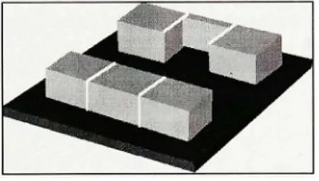
machinery errors. Figure 2.1 shows some types of global and local spot defects occurring
during IC manufacturing process.
Irregular Shapes Smal l Particles Open Lines
Figure 2.1 Global and local manufacturing defects.
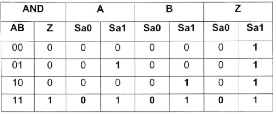
These types of catastrophic defects on a chip can be detected using the traditional "stuck-at" fault model. Over the past decade, the "single-stuck-at" fault model was the most widely used in the industry on digital circuits to detect manufacturing defects. The "single-stuck-at" is a static approximation of a physical defect, in other words, it models all the failures as if all gate level pins or nets connected to the gate as they were stuck or connected or shorted to power or ground. Figures 2.2 and table 2.1 respectively illustrate an AND gate and its single stuck-at truth table. In Fig.2.3, the shaded cells represent the faults that are detected bay applying the corresponding AB combination. As an example, when AB = 11,3 single stuck-at faults are detected: A saO, B saO and Z saO.
This type of fault model is insensitive to clock frequency the device operates on and it assumes that one fault exists at a time during test mode. This makes it applicable under any circumstance, regardless of frequency and time domain. Its simplicity allows a fast computation during Automated Test Pattern Generation and time spent on tester during diagnosis.
A
^,. .n ^
Figure 2.2 Logic AND gate .
Higher operational frequency, higher complexity, smaller area, and lower power consumption usually are the design objectives. Unfortunately, all of these criteria have caused ICs to become susceptible to various yield loss mechanisms which are parametric in their nature and that are not necessarily covered by single stuck-at based test patterns [Sachdev 2007].
The following section 2.3 is a brief summary of a study done by [Hawkings 2003] that sheds light on certain types of IC parametric defects.
Table 2.1 Stiick-at truth table of a 2 input AND gate AND AB 00 01 10 11
z
0 0 0 1 A SaO 0 0 0 0 Sa1 0 1 0 1 B SaO 0 0 0 0 Sa1 0 0 1 1z
SaO 0 0 0 0 Sal 1 1 1 1 2.3 IC parametric defect sParametric failures have been there since the beginning of CMOS technology, but their significance is now more serious and growing. According to [Hawkins 2003], inaccuracies of lithography with CMOS IC nanometer technologies and increasing lack of manufacturing control of circuit parameter variance have shown that allow transistor and interconnect variations. Temperature variation across the circuit as well as power supply levels within the die, and during switching activities may result in inaccuracies that impact circuit quality, and can provoke erroneous functional behaviors and might lead to chip failure.
Interconnect properties include crosstalk errors arise from poor design rule implementation or fluctuations in metal line spacing and width. In the following a description of three different parametric failures is provided: resistive vias, metal mousebites, and metal slivers in ultrathin technologies.
2.3.1 Resistive vias
Nowadays ICs might contain billions of transistors and approximately ten times that number of metal vias. Contacts and vias at the lowest metal level are close to minimum technology feature size. With nanometer technology it is not surprising to see defective vias with elevated resistance.
Crack in metal lines show the same characteristic of a resistive via, even though it is less common to induce failure mechanism on a chip.
2.3.2 Meta l mousebite s
As mentioned above, missing parts of interconnect metal are called mousebites. They can happen during IC manufacturing process due to particles defects, or electro-migration. Figures below show a defect-free and a defective (mousebite) section of interconnect.
Figure 2.4 Defect-free an d a defective interconnect . Extracted from Cook (2003)
Figure 2.5 Zoom-in defectiv e interconnect . Extracted from Cook (2003)
10
Mousebites might have a minor effect on the overall delay on the metal line, but if we divide
a healthy metal line to squares of 0.5 micron each, then if 90% of the middle square as shown
in figure 2.8, is missing, then the new ratio becomes 0.5 |im /0.05|am.
Figure 2.6 Normal Metal line and one with mousebite.
Extracted from Segura (2003)
Figure 2.7 Voided metal resistance (mil) versus percent
metal voiding using Rs = TOmli/sq.
Extracted from Segura (2003)
Assume that sheet resistance is Rj = 70mf^/sq, the resistance of the square with the
Mousebite defect will be equal to Rn = (70mQ/sq)(0.5 |j,m /0.05|am) = 700m^. Therefore,
the original segment of one square was 140mQ and now it becomes 840mQ, yielding an
increase in resistance by a factor of 6.
2.3.3 Meta l Sliver s
Metal sliver defect is due to a metal particle that falls between two metal conductors and slightly contacts the signal line. It can be formed from any of the metal layers used in the fab. With temperature change, this metal can expand and touches or connect the two interconnect lines. This bridge resistance might be permanent and might cause noise on the two signal lines or even cause a fatal functional failure.
2.4 Parametri c failure s du e to defect s
IC parametric defects can lead to parametric failures. Here, we focus on timing failures. Any device with logic network is considered faulty if it does operate correctly at a slower clock speed but fails at the targeted or desired clock frequency.
The cause of failure in a synchronous sequential logic might be extra induced propagation delay on combinational data path reaching a storage element such as a flip-flop or a latch. Each flip-flop has a setup time and a hold time. If the signal propagating through the data path doesn't arrive or be stable before the flip-flop setup time, it is called to be violating the long path timing constraints (setup time violation). In other hands, if the signal is not stable long enough to be captured by the flip-flop it is called to be violating the short path timing constraints (hold timing violation).
According to [Kim 2003], delay defect testing is critical to insure fault free integrated circuits in the overall test strategy. A demonstration of these types of IC defects has been established by Stanford University's Murphy and ELF35 experiments (0.7-and 0.35-micron technology, respectively) on logic circuits designed using standard cells showed that 3 out of 116 defective parts were not detected when tested at lower speed than the expected functional operating speed.
12
2.5 Parametri c timing failure du e to process variatio n
Timing failures can also be caused by regular process variations. During IC manufacturing process, a small natural variation in physical parameters can alter the operating frequency (fmax) and varies in severity from one unit to another. The die location on a wafer, differences in materials and equipments can cause such a variation according to [Hawkins 2003]. It can affect the entire die or can be localized in a part or a block within the die. They might introduce a delay changing without killing the entire die by decreasing the desired frequency the device should operate on.
According to [Chandrakasan 2000], parametric variations might be due from optical effects during lithography processes, resulting in wafer images different from the original layout. It might degrade transistor parameters and might lead to catastrophic manufacturing defects occurring in the poly-silicon layer. Metal interconnect lines can also suffer from variation due to chemical-mechanical polishing (CMP). A chip might function at certain power supply voltages, but not on all its specified VDD range. The die might pass at high speed with high temperature and might fail with colder temperature. It might have windows of pass and fail.
To overcome this issue, engineers should design the chip at a higher frequency targeting all longest path delays called critical path with the worst case conditions. This approach might be very expensive in terms of die size and packaging and difficult to implement and might require extraordinary engineering efforts and time.
2.6 I C delay defects detectio n
"From the SOC testing point of view, test solutions must address new fault models and failure mechanisms caused by manufacturing defects at the 65-nanometer (nm) process node and below" [Kaufman 2008]. In practice, delay faults can be a combination of direct manufacturing defects caused by lithography as resistive shorts and opens and capacitive crosstalk that can impact a local island or functional circuit path within the die, whereas
power supply noise, intra-die temperature distribution, and process variation might cause a global defects that might affect a large part or even the entire chip.
As above underlined, in the real silicon design not all faults can be simply described by the single-stuck-at model that does not include any timing effects. As discussed in the next chapter, this led to the development of delay models that are very similar to the single stuck-at one but thstuck-at also take into considerstuck-ation the timing relstuck-ationship. The applicstuck-ation of these models implies the use of transitions. In the test terminology, AC scan refers to using a scan chain to launch transitions through a combinatorial circuit and capture the response to those transitions within the period of the system clock. However, testing delay faults in a sequential circuit using standard scan (scan based delay testing), has its own limitations, and structural transitional fault model tests might not cover all delays defects leading to a yield escape. Chapter 3 discusses in details the pros and cons of each delay testing approach, be it functional testing, logic built-in self test, as well as scan-based delay testing and the limitations of nowadays ATPG tools.
2.7 Summar y
As shown in this chapter, with nanometer technology, new types of manufacturing defects have risen to the surface, mainly due to the decrease in feature size and probable lack of manufacturing precision of lithography mask. With that in mind, IC manufacturing faults can be classified as catastrophic or parametric. The latter type of faults might occur during manufacturing process due to IC machinery fabrication flaws. These types of faults, that can also be caused by process variafions, might alter the desired fianctional speed on a given ASIC, triggering the necessity of what is called delay testing. These delay defects are not covered by the traditional stuck-at fault model, which is timing insensitive. Delay testing techniques are a must in today ASIC manufacturing process to insure fair test coverage. In the next chapter we discuss in details these delay test techniques and their limitations, and the possibility of enhancing such a test scheme.
CHAPTER 3
EXISTING DELAY TESTIN G TECHNIQUE S 3.1 Introductio n
In this chapter we present and discuss the three main approaches used to detect delay failures, namely: Functional testing. Logical Built In Self Test (LBIST), and scan based delay testing. It shows the pros and the cons, and opens up the discussion about a new testing technique called CDT that complement the actual ones and might boost up the testing coverage to an acceptable level without the need of much engineering effort and time.
3.2 Functiona l testin g
Functional testing consists on applying test patterns derived based upon the functionality of a chip. According to [Bareisa 2008], when used for delay testing, functional test patterns are specifically derived to detect delay failures (caused by defects or by process variations), which most likely affect the longest combinational paths on a chip, or what it is called "the critical paths". According to [Ahmed 2006], the identification of these critical paths, usually performed by using a tool called Static Timing Analyzer (STA), is part of the design flow to guarantee that the chip will work at the desired speed. To derive these functional test patterns for delay testing, test engineers must manually generate these patterns such that they exercise those critical paths (namely, sending a transition along those paths) when applied later on the tester. In order to detect a delay failure, those patterns should be applied at-speed, hence exercising all relevant combinations on the targeted functional blocks using the operation speed or the desired clock frequency. The disadvantages of such approach are the following:
Functional Patter n Developmen t effort : According to [Thibeault 2006], developing suitable efficient functional test patterns requires long and difficult engineering work. Functional at-speed test task is very expensive and requires lots of manual engineering works targeting on some large chips thousands of critical paths rendering it extremely difficult and
somehow impossible to implement. Furthermore, importing such patterns to the tester requires also an extra effort of manual debugging, changing the timing sequences from simulation to tester environment.
High teste r costs : According to [Bareisa 2008], applying functional test patterns to a tester at the desired product speed, using device primary inputs and checking the response at the device primary outputs require a high-end tester that can operate at a very high frequency along with a very high pin counts.
3.3 LBIS T
LBIST is a test approach where most (if not all) test patterns are pseudo-random ones generated on chip, using a linear-feedback shift registers (LFSR), and where the response of the injected patterns are verified on-chip by a signature analyzer (or more information about LBIST structure and design flow, please refer to Annex I). Therefore BIST data exchange with the tester is minimal and drastically reduced. Test costs are generally reduced due to reduced test time, tester memory requirements, or tester investment costs, as most of the tester functions reside on-chip itself Another positive aspect of BIST is that the test can be performed at-speed.
According to [Thibeault 2006], the main disadvantages of LBIST are the area/performance penalty and the extra design effort to deal with: 1) the propagation of the necessary at-speed scan-enable signal (discussed later, section 3.3.1, as this issue is shared by other approaches), 2) the elimination of don't care conditions and multi-cycle paths (when the circuit under test (CUT) requires two or more clock cycles to settle), and 3) the issues related to multiple clock domains and test clock skews peculiar to this test mode.
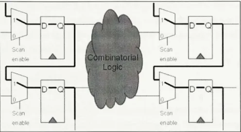
3.4 Scan-base d testin g
This technique is well known and a common design for testability (DFT) application through the entire semiconductor industry and has been used for decades. In this approach, automated
16
scan insertion tools, such as Synopsys TetraMax and Mentor DFTAdvisor, arrange part or all
of the internal flip-flops of a particular device in scan chains. With this architecture in mind,
test patterns generated by ATPG tools are applied to the device under test using the sequence
of events depicted in figures 3.1 and 3.2.
Figure 3.1 Shifting patterns in scan chains.
Figure 3.2 Capturing the response of the combinatorial logic.
The tester puts the chip in test mode by setting the scan enable signal to I on each scan
converted flip-flop. It then shifts each scan pattern serially on the scan primary input. In the
second phase, tester de-assert scan enable for one or two clock cycles (depending on the selected transition launch strategy), bringing back the chip to its normal functionality, allowing the capture of data and the circuit response is stored in the device storage elements i.e. flip-flops. The third phase starts by asserting again the scan enable allowing the stored values in scan chain flip-flops to be shifted out, while shifting in a new pattern. As for the other delay testing techniques, the detection of delay defects requires that transitions are launched and propagated along combinational paths, i.e. there is no dependence between test vectors. With scan-based test techniques, there are two main transition test strategies: the launch on shift (LOS) and the launch on capture (LOC).
3.4.1 Launc h on shift (LOS )
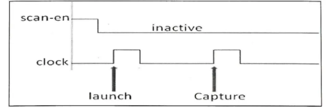
With LOS, the logic value launching the transition is initiated during the last scan shift cycle, when the scan enable signal (scan-en) is still active (figure 3.3). The fault is exercised at this period and the new logic value is captured by the first active clock edge in the capture phase, when the scan-en has been de-asserted (low).
sea n - e n-a c t i v e clocks
I
l a u n c h i n a c t i v e C a p t u r eFigure 3.3 Launch on shift transition dela y fault pattern generation .
LOS takes advantage of a single capture clock pulse to catch the result of the launched logic value; moreover, as the fault is sensitized during the chains load/unload, any of the available clocks can be used. For this reason, a basic scan combinational engine can be used for the test pattern generation, which brings to a much compact set of vectors in a reasonable amount of time. This is the mosfly comparable technique with the single stuck- at ATPG. According
to [Benayahu 2007], the significant drawback is the scan enable signal management. In delay test, the scan enable signal must switch between the launch and capture clock; in design, it fans out to every flip-flop. Therefore, the skew effect plays a relevant role and, if the developed design is not very robust in timing, the balancing of this signal may be required with evident criticalities in routing. Additionally, if the scan enable is slower on the automatic test equipment (ATE) than predicted (different load, more delay induced on the ATE board, induced skew between Scan Enable and CLK, etc.) the device can easily fail also if fault-free. To avoid ATE induced failures, when applying LOS it is recommended to implement the pipelined scan enable technique [Synopsys DFT Compiler Manual].
Otherwise, the scan-enable signal must be routed like a clock signal. Moreover, according to [Benayahu 2007], a very accurate pin-to-pin timing between the enable, in, scan-out, and clock pins must be provided by the tester.
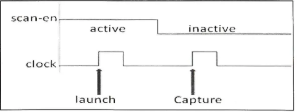
3.4.2 Launc h o n capture (LOC )
With LOC, both launch and capture operations occur when the scan enable signal is inactive, meaning that the chip is in its normal operation mode (figure 3.4) Therefore, the logic value launching the transition comes from the combinational paths, sampled at the regular flip-flop inputs. It exercises the target delay fault at the first active edge of the clock after the scan-enable signal is disabled, and then it captures the corresponding effect at the next clock edge.
scan-Gn
c l o c k
1 i n a c t i v e
1
l a u r
1
^ch Caf1
[
3 t u r -nThe big advantage of LOC is that it relaxes the timing constraints on the scan enable signal, which becomes a regular combinational one. The disadvantage is that a multiple clock capture (sequential) procedure is requested, making the ATPG more compute-intensive and time-consuming. This brings to the generation of more vectors, which may arise potential test data volume issues. The usage of scan compression techniques is strongly recommended to reduce the impact of the pattern count. However, such techniques are often considered too costly in terms of area penalty. In spite of its disadvantages, LOC is often the preferred launch strategy. Once the transition launching strategy is selected, one must also choose the delay fault model on which the test patterns generation will be based.
3.5 Dela y fault model s
There are 2 main fault models that can be used in order to generate the scan-based delay test patterns: the path delay fault and the transient delay fault models.
3.5.1 Pat h delay mode l
The path-delay model is used for testing delay failures on selected paths. According to [Qiu 2004], a circuit is considered faulty if the delay of any path exceeds the specification. As it assumes that the delay fault may be distributed all over a path, this model is most suitable (and used) to detect delay failure caused by process variations. The path-delay fault model requires that the transition traverse a specific path previously defined. Since the number of paths in a real device grows exponentially with the number of nodes in the circuit, it will be impossible to target all the possible combinations of paths because this number may become really huge. Therefore, only the critical paths are addressed when the path-delay model is applied.
20
3.5.2 Transien t fault mode l
The transient delay fault assumes that any delay defect is significant enough to cause a delay failure and that it is associated with (located at) the output of the gate driving the selected node. With this fault model, the single "gate" delay fault represents itself as a pin value of a gate component that works as if it has a "Slow-To-Rise" or "Slow-To-Fall" logic transition, and test patterns are created that passes the transition throughout a single gate only, no matter which path it follows. Test patterns generation in a transition fault model can use the same techniques as stuck-at-faults and can cover theoretically 100% of fault coverage. It requires minor modification for existing stuck-at-fault test patterns generation and simulation tools, and doesn't need any timing analysis. Definitely, transition fault patterns should be injected in the design under test using the highest desired frequency. It can then detect a delay fault on a particular data path, if the data arrival time to the end flip-flop is violating the setup or hold time.
Unfortunately, it must be underlined that the extra-step of applying both 0 and 1 to the identified fault renders the delay test more difficult to compute and more time-consuming. For this reason, the transition delay test coverage of large complex SOCs is typically lower covering, typically 80% of all faults. It is rather more difficult to propagate a transition along the longest paths, as it becomes more difficult to control or observe a particular fault on a given combinatorial site. Nevertheless, the transient delay fault model is the preferred model to generate scan-based delay testing test patterns.
3.6 Curren t DFT techniques limitation s
There are some limitations to the currently used DFT techniques. Some of the limitations are discussed in the following sections.
3.6.1 Smal l delay defec t
Unfortunately it has been shown that timing related defects often introduce a delay which size is less than the at-speed cycle time. According to [Kim 2003], this makes traditional transition fault testing less accurate for this class of faults, as transition ATPG tools attempt sensitizing a fault on the shortest (minimum slack) paths. Transition fault test vectors are therefore unable to individuate a defect which manifests itself on a long circuit path.
3.6.2 Tester s limitation s
It is a well known observation in the semiconductor industry, that even by using state of the art ATPG tools, several gigabits of test data may be required to exercise transition, stuck-at, and path delay faults for a multi-million gate SOC. According to [Pateras 2003], in many cases the testers used in the industry don't have enough memory to store all patterns, forcing test engineers to load and reload test patterns, or use a subsets of the test patterns at a time, hence increasing the test time and cost. Typically every second of test time might cost between 25 to 50 cents, moreover reports from high-end testers used in large Microprocessors, that amortization time for such testers is around $6000 per hour, [Hetherington 1999]. To summarize, large volume of test patterns needed to detect manufacturing defects on a particular ASIC creates a bottleneck for testers in terms of capacity and diagnosis time. As mentioned before, scan compression and LBIST are often considered too complex or costly.
3.7 Conclusio n
The scan-based LOC approach is the dominant delay testing technique, at it eases the scan insertion and design and as it minimizes the area/performance overhead penalty, at the expense of extra test patterns and ATPG CPU time. In this project, our goal is to improve the test coverage of the LOC patterns along the longest critical paths, using DFT techniques, mainly a Capture-less Delay Testing technique that incorporates analog circuitry into the
22
early stages of the design, widening the area of coverage of traditional delay test patterns. Next in chapter 4, we discuss CDT structure and shed light on the major components that make up this novel complementary DFT technique.
CDT (CAPTURELESS DELA Y TESTING ) 4.1 Introductio n
As mentioned in Chapter 3, one of the most difficult test challenges is the ever-growing number of test vectors that need to be applied on the tester to increase the required fault coverage. This is a big challenge in terms of cost and time required for device under test. Multiple types of test pattems are required in order to get high coverage as possible for all sorts of manufacturing defects. The conventional approach is to apply all test pattems until the tester memory is full, LBIST and test compression being often seen as too complex and costly. And as it was also discussed in Chapter 3, LOC transient delay testing is the dominant way to detect faults in nanometer technologies that take into consideration timing related defects.
In this chapter, we present CDT, a recent type of scan based delay testing that requires no additional test pattems, and increase the potential of detecting such delay faults. We discuss the major components that make up this novel complementary delay test technique. It is worth mentioning that CDT was proposed before this master project started. Therefore, CDT is not a contribution of this thesis, which rather covers how to integrate CDT in a traditional design flow.
4.2 CD T Overvie w
CDT (Capture-less Delay Testing) [Thibeault 2006], is a scan-based delay tesfing technique that increases the potential of detecting imperfections that might lead to less bad chips that are tested "Good". This novel approach uses analog test circuitry in the digital world. A redundant circuitry is added on chip, mainly sensors, with a main purpose to test and measure delay affected by defects occurring during manufacturing process. The term captureless means that no logical value is captured during CDT application. As explained later, the most
24
outstanding CDT aspect is that it does not require any addifional test pattems to be loaded in the tester. The overall area and speed penalty of redundant analog testing blocks is minimal. Finally, the CDT potential for automation is partly demonstrated later in this thesis, which should keep low the required additional design effort.
4.3 CD T functionaUty
CDT requires adding sensors at selected scan flip-flop data inputs and scan flip-flop clock inputs. While the device is under test during transition fault pattern shift mode, all data transitions are captured by the sensors located at the input of the modified-to-be CDT scan flip flops.
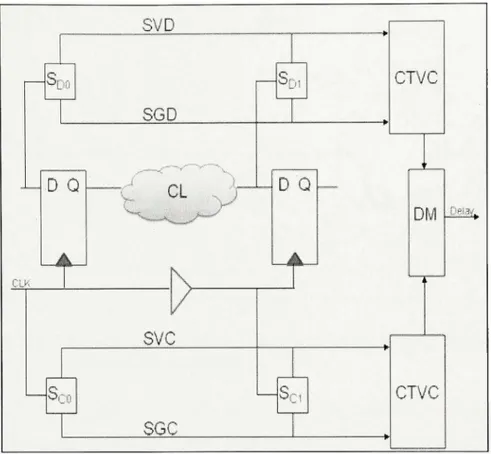
According to [Thibeault 2006], as seen in figure 4.1, the transition capture is performed by the sensors (in this example: SDO and SDI for the data, Sco and Sci for the clock) that transform the voltage transitions into current pulses collected by the parallel power rails (SVD and SGD for the data, SVC and SGC for the clock). These current pulses are then converted back to voltage pulses by the CTVC (Current-To-Voltage Converter) blocks. Finally, the DM (Delay Measurement) block estimates the delay by comparing the clock and the data voltage pulses.
L'l SDO D C
T
•s "•; 'QSVD
SGD /SVC
SGC S.V CTVC 1D Q ~
—Mk . 1 ^ -Sr; ' DM 1 . CTVC Del34Figure 4.1 Scan based CDT architecture.
4.3.1 Implementatio
n of CDT sensor
Each sensor consists of two small inverters twice the minimum size for the target technology
and one small capacitor in series according to [Thibeault 2006]. The dual inverters sensor
structure in figure 4.2 ensures a much balanced and stable voltage to current conversion. The
transient behavior of the cascaded inverter pair is influenced by the intrinsic and extrinsic
related parasitic capacitances. Cgdl and Cgd2 are the gate drain capacitances due to overlap
in Ml and M2. This sensor parasitic model assumes Ml and M2 are either cut-off or in
saturation, which means the transistors are fimctioning in steady state.
26
V i .
-" M II 3£' l 11 ^* ivu
^VtM C t t . SVDc«i_.
('•1
C.:i.i SGDL
^ o Ms i. C'L MdFigure 4.2 CDT sensor implementation: intrinsic (blue), extrinsic (burgundy),
and load (red) capacitances.
Cdbl and Cdb2 are the diffusion capacitances due to the reverse-biased pn-junction. Cw is
the wiring capacitance that depends on the length and width of the connecting wire as it is a
fianction of the fan-out of the gate and the distance to reach those gates. Cg3 and Cg4 are the
gate capacitances of the fan-out gate that depends primarily on the width of M3 and M4
which includes both linear overlap and nonlinear gate capacitances.
The CDT sensor uses small equally sized transistors, with a small capacitance in series that
matches the input capacitance of the inverter driving it. The intrinsic and extrinsic parasitic
capacitances might limit the number of sensors that can be connected on one CTVC block.
The cumulative parasitic capacitances may be a limiting factor when multiple sensors in
chain are switching at the same time, and might require a dynamic compensation to take care
for voltage attenuations on the power rail.
4.3.2 CTV C operatio n
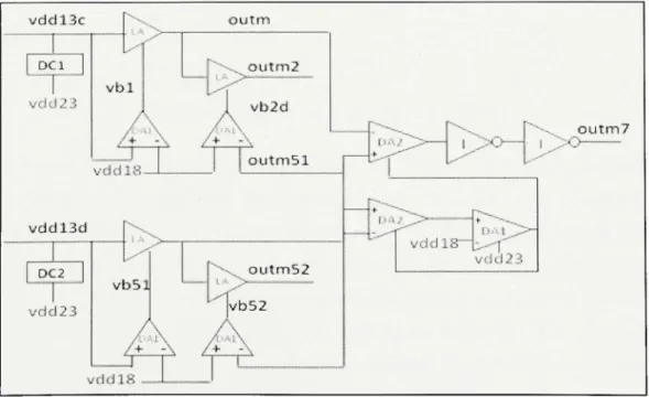
When the CTVC analog block receives the collected current pulses generated by the sensors during switching activity, as transitions happen at the input of the related flip flops chain, it converts the current pulses into voltage pulses ( S V D ^ D V P , SVC^CVP).
The CTVC block as seen figure 4.3, consists of multiple stages, starting from the dynamic compensation on the SVD and SVC current-collecting power rails (DCl, DC2), the pre-amplification stage using a low gain amplifier (LA), calibration circuitry (DAI), a current to voltage conversion stage formed with a current mirror load differential amplifier (DA2), and a final buffering stage consisting of two inverters (I) in series. The low level transistor schematics for each sub-block are fiarther analyzed and explained in the upcoming sections.
vdd13c DCl vdd 2 3 v b l /
fr
v d d l S -v d d l 3 d |_£e2_J vdd 2 3 1 A > . vcWJg o u t m |"'^-^.s.^outm2 vb2ciJ\
o u t m S la
'""\ outmS 2 i.. A ^ P A i I > o I po-o u t m 728
4.3.3 Dynami c compensatio n
The dynamic compensation block works like a bleeder that compensates for any potential attenuation on the power rails voltages. It forms an internal on the fly compensation during switching activity of the sensors. The implementation of the DC block is seen in figure 4.4.
vr2— vr3 VdctlSc™, vr4— V d d l S c -vr8— V>i ''*' ^^^^^ iH, m Vddl3c •1^ i m200 mBOO m400 mSOO Vdd23
Figure 4.4 Dynamic compensatio n o n Vddl3c.
As the voltage decrease on the vddl3c node, when transitions occur at the input of multiple sensors, the dynamic compensation structure rectifies vddl3c pulling it up to vdd23. When both differential amplifier inputs are at the same potential, the comparison between vddI3c with one of the different internally generated voltage sources (vr2-vr8) leads to logic 0 that tums the related PMOS transistor on as it enters the resistive region of operation. Hence, the current flows through the active transistor and pulls up the depleted vdd 13c. This helps to reduce the impact of the number of simultaneously switching sensors (SSS) on the measured delay at the final DM stage.
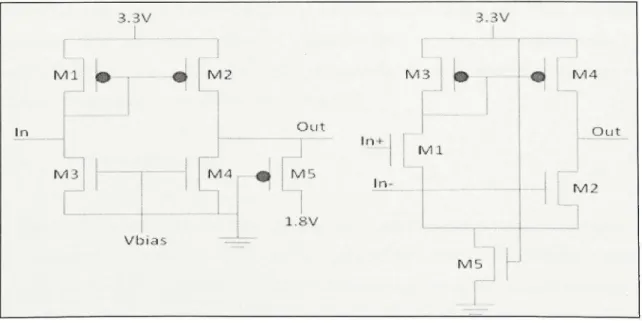
4.3.4 CTV C 1s t stage: Low Gain Amplificatio n
The low gain ampHfier L, as seen in figure 4.5(a), is biased by the differential amplifier DAI which is twice the transistor sizing of DCl. One way to control the quiescent current is to sense and feedback a copy of the input current. The opted way limits the variation in the quiescent current by designing the amplifiers to have low gain. The quiescent current is controlled by the gate-source voltages on the M3-M4 NMOS transistors of LA, which in turn is confroUed by the output of the differential amplifier DAI. Therefore, reducing the preamp gain reduces the variation of gate-source voltages and the quiescent current for a given variation in the offset voltages. Also a second LA amplifier is added as a load on the outm51 node, for offset calibration purposes. As Ml is connected in diode mode, it mirrors the current from M3 and flows into transistor M2 through M4. M5 is always branched always in saturation as an output PMOS resistor bleeder.
30
4.3.5 CTVC 2n d stage: Differential Amplificatio n
A current mirror load differential amplifier, as seen in figure 4.5(b), is used in the CTVC block to produce an output voltage proportional to the input current. The amplifier has a current mirror load so any imbalance in the drain currents of Ml and M2 causes the output of the differential amplifier to swing either towards Vdd23 or Vss.
When Vin- is larger than Vjn+, the current in M2 is larger than the current in Ml as VGS2 > VGSI. The current in Ml flows through M3 and is mirrored by M4. This causes DA2 output to go towards Vss until the current in M2 equals the current in M4. The internally generated reference voltage outm51 is deliberately connected on the inverting node of DA2 in order to achieve maximum gain. Since M3 is connected in a diode configuration it has a lower resistance than M4 hence the gain from Vjn- to the output out is larger.
The amplifier operates as a current to voltage converter due to its near zero input and output impedance. The self-biased differential amplifier DA2 receives the voltage outm, as previously seen in figure 4.3, on the inverting input while its non-inverting input receives the reference voltage outm51 which is always grounded.
4.3.6 CTVC Bufferin g Stage
As the CMOS inverter can be modeled as a dynamic equivalent output resistance ro, there are more aspects that need to be taken care of, such as the intrinsic and extrinsic parasitic capacitances that play a major role during the switching activity of the cascaded inverters as seen in figure 4.3.
The resulting current to voltage conversion at the output of DA2 gets buffered through a cascade of two inverters in series generating the final DVP (data voltage pulse) and CVP (clock voltage pulse) output voltages to be later processed by the delay measurement DM block. DA2 and the cascaded inverters at the final stage form a high speed input buffer which
transforms the input signal that might have uneven slow-to-rise and slow-to-fall transitions
into a clean digital signal with correct pulse width and level.
4.3.7 Dela
y measurement stage
The delay between the incoming voltage pulses from the data path is then measured against
the voltage pulse received from the clock network. As seen in figure 4.6, the delay
measurement is taking place between the falling edges of the CVP and DVP voltage pulses
by the delay measurement (DM) block.
CLK A B SVC SVD CVP DVP : -'^ Delay ; 1 X '
'1
i—1 . Delay'1
Figure 4.6 CDT Timing Diagram.
The delay measurement can be done on chip or off-chip during wafer probing. With this
approach we can estimate the propagation delay of the combinatorial clouds and therefore the
ICs maximum achievable clock frequency. When the CUT's frequency is exceedingly lower
than specified frequency, the circuit under test is declared faulty. It is worth mentioning that
the delay measurement differential approach should mostly compensate for any offset error
along the path. CDT limitations are discussed in [Thibeault 2006].
32
4.4 Advantage s o f CDTP (Capture-less Dela y Testing Patterns )
The majority of DFT engineers are using a combination of stuck-at and LOC transition fault model pattems to achieve an acceptable level of fault coverage. Traditional ATPG tools fail to cover those hard to control/observe faults that lie on the longest critical paths. It's much more convenient to integrate CDT in the architecture along those critical paths then spending time writing functional path delay pattems to exercise the faults. CDT might detect potential faults and allows for seamless integration with current techniques, as DFT engineer can aim for higher if not near perfect test coverage with a very reasonable amount of area/speed overhead.
As memory tester is often limiting the number of test pattems that can be applied. CDT then becomes a very efficient way to boost the delay fault coverage without requiring any additional tester memory. CDT takes advantage of the fact that no data is captured to transform the intermediate values contained in the scan chains during the shifting (in and out) into CDT test pattems.
The CDT pattems can be characterized as:
C^'rPatterns — (Sc — 1) X PattemSfraditional (4-1)
Where Sc in the total number of scan flip flops in one scan chain.
As an example, if there are 5000 scan test pattems, 1 scan chain of 1000 scan cells; it creates around 5 million additional (CDT) test pattems. This means that the number of delay test pattems can be increased by order of magnitude.
It is important to disable all sensors during normal functional mode in order to eliminate any addifional dynamic or static power consumption. The CDT architecture allows such important low power feature, as it consists of multiple separate power domains for the CTVC
and DM blocks as well as the data current pulses (SVD, SGD) and the clock related current pulses (SVC, SGC).
4.5 Conclusio n
CDT is a Top-Off technique that uses the already generated transition faults model pattems. This complementary technique doesn't require any additional pattems to be generated nor stored, hence no additional tester memory load and no restrictions on the CPU computation time. CDT is an at-speed testing technique. It captures transitions at the input pin of a CDT Scan Flip Flop during LOC shift mode, and allows the test engineer to measure the delay differences between data paths and clock network, hence giving an accurate estimation of the highest frequency the circuit under test can operate on. It doesn't require any post layout information and it can be inserted during early stages of DFT / ATPG flow. Next in chapter 5, we discuss the timing based delay distribution of the left undetected faults by traditional mainstream ATPG tools, the ones we will target with CDT.
CHAPTER 5
Timing Based Delay Distributions o f Transition Undetecte d Fault s Mode l 5.1 Introductio n
Any testing that is not aware of the delay that might occur due to process variation or any other defects in nanometer technology is not complete. A small delay on a critical path might cause a timing failure that can render the chip unusable or operate at a lower frequency. Commercial ATPG tools usually exercise transition fault test pattems on the shortest path, and are timing unaware, as transition ATPG technique attempts sensitizing a fault on the shortest (minimum slack) paths without incorporating the SDF annotation timing. Furthermore, since the ATPG tool doesn't consider the timing constraints and the actual delays of the devices and interconnects in a given design, a transition test pattern that detects a fault on a long path might fail to detect the same fault if that path was critically timed.
In the industry, according to [Davidson 2007], test coverage of 75-85% for transition fault pattems is considered acceptable when factoring in time, cost and reliability of the test. Hence, CDT implementation might bridge the gap by complementing the LOC transition fault model and further improving the test coverage with minimum time and engineering effort, at no extra tester cost. This chapter discusses this issue in details by analyzing the delay distribution of the left non-covered faults by conventional ATPG tools such as Mentor Fastscan. The ATPG process is targeting low cost testers and meant to respect reasonable industry standard test abort limit.
5.2 Sca n based structural test technique s
Scan-based structural tests are widely used in the industry for their cost/coverage test effectiveness versus at-speed functional test. Transition fault models targets for slow-to-rise and slow-to-fall the output on each gate in the design. Path Delay targets the full path from the start point (output of a flip-flop) to the end point (input of a flip-flop) of the total delay
(gates and interconnects) on a specific circuit path. Detecting a delay induced defect on a chip, transition faults and path delay faults models are so far effective in producing good fault coverage. Unfortunately they have some limitations that are discussed in chapter 3.
Transition fault test are applicable on one clock domain, assuming a fixed cycle time. When a transition occurs and reaches the end point and being captured and observed, a defect might be detected if it doesn't meet the timing slack of the exercised and observed circuit path. Relatively to the clock domain, if the slack of this particular circuit path is big, the delay defect might not be detected. This defect escape might introduce a failure later in the life cycle of the chip. The quality of the chip is then reduced, and might trigger a costly recall.
A small delay defect that might occur on a short path might have subsequent aging failure on a chip, while a defect occurring on the longest path might have a catastrophic immediate effect on the correct operation of an integrated circuit. By using current commercial ATPG tools, such a defect on the longest path might be left undetected with transition fault models. In this chapter we will focus on the longest path fault detection and its impact on the overall test coverage.
5.3 ATPG methodology
In this study we determine the ATPG undetected faults and observe where they lie in the timing domain of each related path. For simplicity we used a single clock domain design, especially that transition fault model requires one clock domain in each scan chain to be exercised and observed one at a time. A delay distribution of the undetected faults paths using Launch-On-Capture (LOC) transition fault model is evaluated. In the following figure, the implementation flow is described. A set of tools using Perl scripting is implemented at each stage of the flow to extract and process data.
In this study, we target some of the Politecnico di Torino circuits belonging to the Intemational Test Conference (ITC99) benchmark suite that were meant to be used for
36
experimentation on DFT and ATPG. Those benchmarks correspond to synthesizable
RT-level descriptions of different size, complexity, and type [ITC 99 Benchmarks].
,/*! V ^ V T&tVaiDr5
X
Uncovered(i) • Coveredy) >"ODES (3 KLOC} ; 3 ! {LOS})~CDT 3{LOC}; 3f{LOS > Paths (J m n-pdfir Um3>.pdf i}''Cmin-Figure 5.1 Path delay distribution extraction flow.
Perl scripts were created to mn DFT /ATPG processes that are applied on the ITC99
benchmark b05 and to analyze results. It determines the min and max path delays of those
nodes that are non-covered by LOC. It can further analyze and determine the final Delay
distribution of any selection of covered nodes in relation to non-covered ones. This
methodology allows for proper investigation of the placement of the undetected faults along
the respective paths as well as it shows the occurrences of the suitable path transition delays
which is crucial to understanding the switching activity of the CDT sensors that are going to
be inserted at a later stage.
5.4 Simulate d implementation step s
Scan chains insertions are implemented by DFTAdvisor in the design and Mentor Graphics Fastscan ATPG tools using transition fault with Launch-On-Capture and Launch-On-Shift. Fastscan is then used to report all Fan-in and Fan-out of all non-covered nodes on both LOC and LOS. A set of Perl scripting tools compare the LOC undetected faults and the LOS undetected ones to create the following lists: 1) the list of nodes non-covered by LOC but covered by LOS (those are the nodes we want to cover with CDT and from which the destination FFs, where sensors are added, are determined), 2) the list of nodes non-covered by LOS but covered by LOC, and 3) the list of nodes that are non-covered by both.
After generating the destination FF file, we use the paths links and mn it in Prime-Time Static Timing Analyzer, with type 'Max" meaning we are taking into account the maximum delay. The worst case process comer is used, for slack timing calculation. Parsing through the STA report, the arrival time for each path is calculated. The minimum path delay umin-pd(i), and the maximum path delay umax-umin-pd(i), of all the paths passing through the same node i are measured. The number of occurrences of all minimum and maximum path delays, are then computed on all undetected nodes.
As can be seen in figure 5.1, the previous procedure is repeated for all the covered nodes to calculate their path delay occurrences. For each covered node j , we respectively define cmin-pd(j) and cmax-cmin-pd(j) as the minimum and maximum path delay of all the paths passing through this node.
5.5 Simulatio n result s
5.5.1 Minimu m path delay distribution o f non-covered fault s
The following chart shows the delay distribution of all the shortest paths, namely all Umin-pd(i) values, along all non-covered faults. The fastest path of all shortest paths namely
38
min(umin-pd(i),) is taking 18.7% of the cycle period to arrive at the (to be inserted) CDT
sensor. Whereas the slowest path max(umin-pd(i), V i) is taking 77.1% of the clock cycle
period to arrive at the to be inserted CDT sensor that lies at the input of the destinafion FF.
25 -1 20 -5« '1 C s 1 1 1 0 -O 5 -0 - 1
Delay Distribution o f Min. Paths of I'ncov faults, uniin-])<l(i)
•
/ \
•f \
5 20 40 GO 80 100
Path Delay (%T ) 120