HAL Id: hal-02335357
https://hal.archives-ouvertes.fr/hal-02335357
Submitted on 28 Oct 2019
HAL is a multi-disciplinary open access
archive for the deposit and dissemination of
sci-entific research documents, whether they are
pub-lished or not. The documents may come from
teaching and research institutions in France or
abroad, or from public or private research centers.
L’archive ouverte pluridisciplinaire HAL, est
destinée au dépôt et à la diffusion de documents
scientifiques de niveau recherche, publiés ou non,
émanant des établissements d’enseignement et de
recherche français ou étrangers, des laboratoires
publics ou privés.
Nonlinear noise modeling of a PHEMT device through
residual phase noise and low frequency noise
measurements
Olivier Llopis, J Juraver, B. Tamen, F. Danneville, M. Chaubet, A. Cappy,
Jacques Graffeuil
To cite this version:
Olivier Llopis, J Juraver, B. Tamen, F. Danneville, M. Chaubet, et al.. Nonlinear noise modeling
of a PHEMT device through residual phase noise and low frequency noise measurements. IEEE
International Microwave Symposium, May 2001, Phoenix, United States. pp.831-834. �hal-02335357�
Nonlinear noise modeling of a PHEMT device through residual
phase noise and low frequency noise measurements
O. Llopis, J.B. Juraver, B. Tamen*, F. Danneville*, M. Chaubet**, A. Cappy*, J. Graffeuil
LAAS-CNRS, 7 av. du Colonel Roche, 31077 Toulouse FRANCE
*IEMN, Avenue Poincaré, BP 69, 59652 Villeneuve d'Ascq, FRANCE
**CNES, 18 av. Edouard Belin, 31401 Toulouse, FRANCE
Abstract The phase noise generated by a FET device is
investigated using transmission and reflection residual phase noise measurements. This approach helps in locating, in the intrinsic device, the low frequency noise sources which are responsible for these phase fluctuations. On the basis of these experiments, a new nonlinear noise model of the FET is proposed. This model is able to describe a phenomenon that has been observed, but never modeled in the past : the dependence of the baseband noise on the microwave input power.
I. INTRODUCTION
The oscillator phase noise has been, for more than 30 years, one of the most difficult and less understood problem in microwave electronics. The high frequency white noise has been firstly proposed as the possible cause of oscillator’s frequency fluctuations [1]. Then, the transposition of the transistor low frequency (LF) noise (or excess noise) has been recognized as the main source of frequency fluctuations in most microwave oscillators [2,3]. The main goal of the microwave scientists has then been to model this transposition of LF noise into microwave phase noise. This has been done successfully with simplified models [4] for a qualitative description of the mechanisms, or more accurately using dedicated CAD approaches [5,6]. However, each of these techniques supposes that the LF noise sources in the device are well known and can be localized in the intrinsic non-linear model of the transistor. This is, in our opinion, the most difficult step in an oscillator phase noise modeling.
The reason is that the location of a noise source in the nonlinear model is of prime importance. Indeed, in a linear design, a physical noise source in the device can be replaced by an equivalent noise source (almost) anywhere else in the device. On the contrary, in a nonlinear design, a given noise source will induce the fluctuations of some nonlinear elements and these fluctuations will strongly
depend on the location of the source with respect to these elements.
It is therefore essential to determine an experimental procedure which can help in the localization and in the extraction of these intrinsic noise sources. In this paper, residual phase noise measurements and drain current LF noise measurements are used to this purpose. These measurements are performed at different input microwave levels, ranging from the linear operation to the strong compression regime. Moreover, reflection mode residual phase noise measurements are performed and help in the understanding of, as an example, the gate related noise mechanisms. On the basis of these results, a new nonlinear noise model of a commercial PHEMT device is proposed. The main interest of this model is in its ability to describe the dependence of the LF noise on the microwave input power.
II. EXPERIMENTAL SET-UP
The experimental set-up is depicted in Fig. 1. The residual phase noise data (or open loop phase noise) has been preferred to the measurement of an oscillator phase noise because a better control of the experimental set up is provided by this measurement mode [7]. The transistor behaves as an amplifier, there is no loop condition and a measurement is possible from the nonlinear regime down to a perfectly linear regime while, in the oscillator case, the linear regime cannot be easily investigated. Moreover, these two types of phase noise are not so much different : it is the amplifier phase noise which is directly converted into oscillator’s frequency fluctuations in an oscillator loop [8].
The two parameters that are being measured are the PHEMT phase fluctuations, on 50 Ω input/output loads, and the PHEMT drain current fluctuations. The whole experiment is performed in a shielded environment, and
the device is battery biased. The input source is a low noise dielectric resonator oscillator, also battery biased, and the experiment is optimized to reject the AM and FM noise of this source. Thanks to a two mixers technique and an associated cross-spectrum analysis, the noise floor of the residual phase noise measurement is much lower than the phase noise levels that are measured on FET devices. This noise floor is in the range of -175 dBc/Hz at 10 kHz offset. Mixer 2 FFT spectrum analyser Faraday's shielding 50 dB Mixer 1 Att. Att. 50 dB A B LFG φφ DRO FET Rd Vd0 Vg0 Rg 40 dB
Figure 1 : Experimental set-up for the residual phase noise
and LF noise measurements
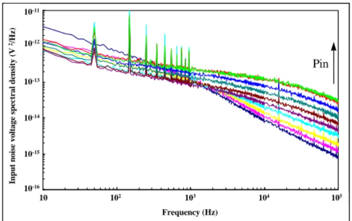
III. LF NOISE AND PHASE NOISE MEASUREMENT The measured LF noise data are depicted in Figure 2. The LF drain current noise is systematically transformed into an equivalent voltage noise source on the gate, by measuring the FET LF gain (or transconductance) under non-linear operation. A strong change is observed on this spectrum between the linear regime and the compression regime, both in amplitude and shape. Such a behavior has been already discussed in earlier papers [9,10,11]. It is responsible for the inaccuracy of the phase noise calculations performed with the gate voltage excess noise model. The change of the equivalent noise spectrum with the input microwave power can be understood through the following equation :
Sv = [k1(Vgs,Vds)]2 S1 + [k2(Vgs,Vds)]2 S2 + ... (1)
where Sv is the total equivalent gate noise spectral density,
Sn (n = 1,2...) are the intrinsic noise sources spectral
densities and kn(Vgs,Vds) are the transfer functions
between these sources and their representation on the gate electrode. These transfer functions can be nonlinear and, in this case, when the microwave signal is superimposed on the device, they are modified. In these conditions, the effect of some noise sources can be increased, with respect to other sources. 1,E-16 1,E-15 1,E-14 1,E-13 1,E-12 1,E-11
1,E+01 1,E+02 1,E+03 1,E+04 1,E+05 Frequency (Hz)
Sv (V^V/Hz)
Pin
10-16
10-11
Input noise voltage spectral density (V
2/Hz) 10-12 10-13 10-14 10-15 10 102 103 104 105 Frequency (Hz) Pin
Figure 2 : Measured equivalent input LF noise spectral density
of the PHEMT device versus different input microwave power levels at 3.5 GHz (from the linear regime up to compression : -8 dBm < Pin < + 4 dBm) -160 -150 -140 -130 -120 10 100 1000 10000 100000 Fréquence (Hz)
Bruit de phase résiduel (dBrad/Hz)
Pin 10 102 103 104 105 -120 -130 -140 -150 -160
Phase noise (dBrad/Hz)
Frequency (Hz)
Pin
Figure 3 : Measured residual phase noise of the PHEMT device
at 3.5 GHz (same conditions than in Fig. 2)
The only rigorous solution to this problem is to combine different measurement data to extract the intrinsic noise sources Sn. We use, to this purpose, residual phase
noise data, both in transmission and reflection mode. The transmission residual phase noise data for the same device are depicted in Figure 3. These spectra clearly show that the observed LF noise variations versus the input microwave power are also observed on the phase noise data. Moreover, at high input power, a strong generation-recombination (G-R) noise source, revealed by a strong bump near 10 kHz, is predominant in both measurements. This is typical of what we have already observed on other HEMT devices [9,10]. Also, this similarity between the LF noise and the microwave phase noise at high input power is the evidence of a strong correlation between these two fluctuation phenomena. It is due to the predominance of a specific LF noise source in
the LF to phase noise conversion process. Our main goal has thus been to find a model able to describe the rising influence of such a noise source with the increasing microwave power.
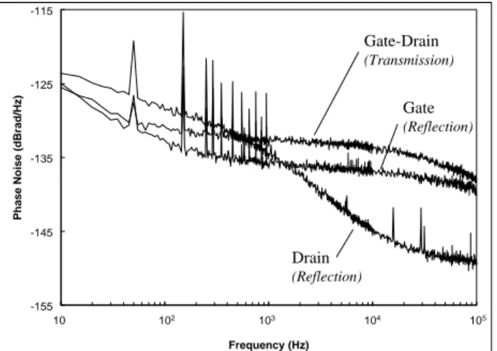
The first step is in finding the location of such a noise source in the nonlinear model of the transistor. To this purpose, the information given by reflection mode residual phase noise measurement is particularly interesting. This new phase noise measurement mode consists in using a circulator to separate the reflected wave from the input wave on the FET gate or drain port, thus allowing the phase noise of the reflected wave to be measured. The phase noise of a ferrite circulator is much lower than a GaAs transistor noise and there are no special difficulties in such an experiment, except that the power level on the mixer RF port is lower than in the transmission case because of the absence of any amplification through the DUT.
The result of such an experiment is depicted in Figure 4. The PHEMT residual phase noise is shown, for a high microwave input power level of 4 dBm, on three measurement configurations : reflection on the gate electrode (phase fluctuations of S11), reflection on the
drain electrode (phase fluctuations of S22) and transmission
gate-drain (phase fluctuations of S21).
-155 -145 -135 -125 -115 10 100 1000 10000 100000 Frequency (Hz)
Phase Noise (dBrad/Hz)
10 102 103 104 105 Drain (Reflection) Gate (Reflection) Gate-Drain (Transmission)
Figure 4 : Measured reflection and transmission phase noise at
high level (4 dBm) ; reflection on the input (gate) and on the output (drain).
When compared to the transmission phase noise data, the reflection phase noise reveals a very similar spectral shape at the input and a much different at the output. Actually, the spectral shape observed at the output is similar to the one observed in transmission at low input power. Two major remarks can be made from these results. The first one is that a strong fluctuation of the gate-source reactance takes place in the device, which is
responsible for the high level of phase noise in reflection on the gate. The second one is that the high G-R noise source observed at high level on the LF noise or on the transmission phase noise spectra is predominant only if the microwave signal is injected on the PHEMT gate electrode.
These remarks demonstrates the existence of a gate related LF noise source, associated with a gate related nonlinear element able to translate the effect of this LF source into phase fluctuations. In various papers [4,10], this noise source was described as a voltage noise source in series with the gate electrode and the gate capacitance was suspected to be the main nonlinear element in the device responsible for the transposition of this LF noise into phase noise. Unfortunately, this model is unable to explain the strong changes in the spectral shapes depicted in Figures 2 and 3. It is therefore essential to determine which gate related nonlinear element of the PHEMT equivalent circuit can be responsible for this behavior. There is effectively one parameter, which is often considered to be linear, but which actually features variations with the gate bias : the input channel resistance Ri. A multi-bias small signal model extraction procedure shows that this resistance features bias related variations that are inversely proportional to the one of the transconductance gm, which is a strong device nonlinearity.
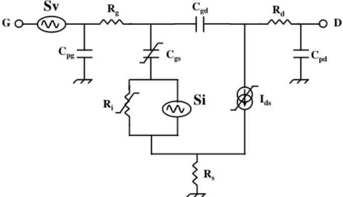
IV. PHEMT NON LINEAR NOISE MODELING The model used is depicted in Figure 5. It is a classical laboratory extracted FET nonlinear model, in which a polynomial Ri(Vgs) nonlinearity is added.
The LF noise is described with two sources : one source is the classical voltage noise source in series on the gate and the other one is a new current noise source in parallel with Ri(Vgs).
The association of a current noise source with Ri(Vgs) leads to an equivalent gate voltage noise which depends on the microwave input power, simply because the value of Ri depends on the microwave input power. Therefore, such a noise source is predominant at high microwave power.
The total LF noise measured has been shared between these two sources, in order to obtain the better possible fit of the measured noise data. Concerning the Ri associated source, its spectral characteristics can not be determined from the LF noise measured on the quiescent device. Therefore, the LF noise data measured at different high microwave level have been used to model this source. On the contrary, the influence of the classical gate voltage noise source is predominant at low microwave power and the LF noise data measured on the quiescent device is used in this case to model it.
Sv Si Cpg Rg Cgd Cpd Rd Cgs Ids Ri Rs G D
Figure 5 : PHEMT nonlinear model, including the two LF noise
sources Sv and Si -170 -160 -150 -140 -130 -120 10 100 1000 10000 100000 Fré que nce (Hz) B ruit d e pha se rés idu el (dBrad/Hz) 10 102 103 104 105 -120 -130 -140 -150 -160 -170
Phase noise (dBrad/Hz)
Frequency (Hz) Pin
Figure 6 : Modeled transmission residual phase noise of the
PHEMT device (same conditions than in Fig. 3)
V. PHASE NOISE SIMULATION
The PHEMT phase noise is simulated using a commercial harmonic balance software and a modulation approach [5]. The conversion coefficients of each of the two noise sources into phase fluctuations are calculated through a quasi static perturbation of the nonlinear steady state. Then, the total phase noise is the sum of these two contributions, which are supposed to be uncorrelated.
The result of this phase noise modeling is shown in Figure 6. The increase of the phase noise at high input power is well described. Compared to the results of Figure 3, the phase noise variation with the microwave power is now very similar ; the only difference is in the absolute level of phase noise which is a few dB lower on the simulated values than on the measured ones. This can be due to the difficulties met during the model extraction : the phase noise mainly depends on the gate charge and the input channel resistance nonlinearities, and these two elements are not the easiest ones to model.
VI. CONCLUSION
The phase noise modeling of FET devices has always been a difficult task and no device nonlinear model able to describe the noise variations with the microwave power was available, up to now. In this paper, the generation of the phase fluctuations near the gate electrode of a PHEMT device is demonstrated using various residual phase noise measurements (reflection and transmission). A new nonlinear model of the device is then proposed, including two low frequency noise sources. This model solves, for this device, the problem of the LF noise dependence on the microwave power.
REFERENCES
[1] K. KUROKAWA, « Some basic characteristics of broadband negative resistance oscillator circuits », Bell Systems Technical Journal, July-August 1969, pp. 1937-1955. [2] J. GRAFFEUIL, A. BERT, M. CAMIADE, A. AMANA,
J.F. SAUTEREAU, « Ultra low noise GaAs MESFET microwave oscillators » Noise in Physical Systems and 1/f Noise Conf., 1983, pp. 329-332.
[3] M. POUYSEGUR, J. GRAFFEUIL, J.F. SAUTEREAU, J.P. FORTEA, « Comparative study of the relation between device low frequency noise and oscillator phase noise for GaAs MESFETs », 1987 IEEE MTT-S Digest, pp. 557-560. [4] H. J. SIWERIS, B. SCHIECK, “Analysis of noise
upconversion in microwave FET oscillators”, IEEE trans. on MTT, vol 33, n° 3, pp. 233-242, 1985.
[5] V. RIZZOLI, F. MASTRI, D. MASOTTI, “General noise analysis of nonlinear microwave circuits by the piecewiese harmonic-balance technique”, IEEE trans. on MTT, vol 42, n° 5, pp. 807-819, 1994.
[6] J. M. PAILLOT, J.C. NALLATAMBY, M. HESSANE, R. QUERE, M. PRIGENT, J. ROUSSET, « A general program for steady state, stability and FM noise analysis of microwave oscillators » 1990 IEEE MTT S. Digest, pp. 1287-1290.
[7] P.A. DALLAS, J.K.A. EVERARD, “Measurement of the cross-correlation between baseband and transposed flicker noises in an GaAs MESFET” 1990 IEEE MTT-Symp. Digest, pp. 1261-1264.
[8] D. B. LEESON, « A simple model of feedback oscillator noise spectrum » Proc. of the IEEE, vol 54, n° 2, Feb. 1966, pp. 329-330.
[9] O. LLOPIS, J. VERDIER, R. PLANA, J. GRAFFEUIL, "Low frequency noise in FET devices operated under nonlinear conditions ; consequences on oscillator phase noise", Proceedings of the 1995 EuMC, pp. 285-289. [10] J. VERDIER, O. LLOPIS, R. PLANA, J. GRAFFEUIL,
"Analysis of noise up-conversion in microwave FETs oscillators" IEEE trans. on Microwave Theory and Tech., vol 44, n° 8, aug. 1996, pp. 1478-1483.
[11] H.J. SIWERIS, B. SCHIEK, "A GaAs FET oscillator noise model with a periodically driven noise source", 1986 EuMC Proceedings, pp. 681-686.