Introducing Positive Envelope Feedback – A New Method for
Linearity Improvement in Radio Frequency Integrated Circuit
Power Amplifiers
by
Smarjeet SHARMA
THESIS PRESENTED TO ÉCOLE DE TECHNOLOGIE SUPÉRIEURE
IN PARTIAL FULFILLMENT FOR THE DEGREE OF
DOCTOR OF PHILOSOPHY
Ph.D.
MONTREAL, MARCH 13, 2020
ÉCOLE DE TECHNOLOGIE SUPÉRIEURE
UNIVERSITÉ DU QUÉBEC
© Copyright reserved
It is forbidden to reproduce, save or share the content of this document either in whole or in parts. The reader who wishes to print or save this document on any media must first get the permission of the author.
BOARD OF EXAMINERS (THESIS PH.D.) THIS THESIS HAS BEEN EVALUATED BY THE FOLLOWING BOARD OF EXAMINERS
Mr. Nicolas Constantin, Thesis Supervisor
Electrical Engineering Department at École de technologie supérieure
Mr. Guy Gauthier, President of the Board of Examiners
Systems Engineering Department at École de technologie supérieure
Mr. Vahé Nerguizian, Member of the jury
Electrical Engineering Department at École de technologie supérieure
Mrs. Lyne Woodward, Member of the jury
Electrical Engineering Department at École de technologie supérieure
Mr. Serioja Tatu, External Evaluator
Centre Énergie Matériaux Télécommunications at INRS, Montréal
THIS THESIS WAS PRESENTED AND DEFENDED IN THE PRESENCE OF A BOARD OF EXAMINERS
JANUARY 24 2020
DEDICATION
FOREWORD
The work presented in this thesis presents my original research work that was carried out from 2012 to 2019 at École de technologie supérieure, Montreal as part of my master’s-doctoral integrated-program studies under the supervision of Professor Nicolas Constantin and in collaboration with the Ottawa R&D division of Skyworks Solutions, Inc., a U.S.-based world leader in the area of radio frequency integrated circuits for wireless communication. The objective of this research work is to address the linearity-power efficiency trade-off in power amplifiers (PAs), a subject of extensive investigation and much scholarly treatment since the advent of vacuum tube power amplifiers in the early part of the twentieth century and yet never short on excitement in terms of new and innovative methods that continue to be proposed towards further improving power amplifier performances. My doctoral research work introduces and demonstrates one such innovation based on an original positive envelope feedback circuit technique in Radio Frequency Integrated Circuit (RFIC) PAs. Further, my doctoral research work introduces an analytical three-port power amplifier representation to aid the design and implementation of envelope-dependent PA biasing techniques, including positive envelope feedback PAs, in practical scenarios that benefit from the availability of closed-form equations for predicting PA performances and PA biasing requirements. One such scenario, shown for the first time through my doctoral research, demonstrates using the 3-port power amplifier representation for the embedded self-calibration of PAs within the mobile unit to compensate against part-to-part variation of RFIC PA performances. The results of my doctoral research work have been submitted to two journals (one published and one currently under revision), published in three patents (two granted and one under provisional application) and one conference paper (awarded “Best Student Paper”). Multiple additional journal manuscripts are currently under preparation for submission. Another journal, two conference papers (including one as a second author) as well as various posters have also been presented and highlight contributions directly or indirectly stemming from the research work conducted during my doctoral studies.
ACKNOWLEDGMENT
It would hardly be an overstatement to say that the research work presented in this thesis would have been impossible without the constant help, guidance and encouragement given by my thesis supervisor, Professor Nicolas Constantin. From working very late hours together to spending entire weekends (including during the holidays) trying to troubleshoot designs, reviewing test measurements and drafting technical documents – my years in academia during the last few years of graduate studies have truly been a learning experience, and in no small part because of Professor Constantin. Whatever little that I have learned regarding the nuances associated with conducting research is largely due to his excellent tutelage, and I am extremely grateful for it.
I would like to express my appreciation to the members of my thesis evaluation jury for accepting to review this document, and for taking time out to examine the research work presented here. I would also like to express my gratitude to the staff at Skyworks Solutions, Inc. for their assistance with various aspects of my work, as well as their insights into industry practices that I was exposed to during (as well as after) my time at the R&D Division of their Ottawa design center. My thanks are due to the staff at the Laboratoire de communication et d’intégration de la microélectronique (LACIME) and the staff at the Electrical Engineering Department of ÉTS, who have both always been forthcoming with their help. I would also like to acknowledge the support of ÉTS Excellence awards for international students – Master’s-PhD Award, CMC Microsystems Canada, MITACS Canada and the Natural Science and Engineering Research Council (NSERC), Canada.
My life at ÉTS, and in Montreal, has been enriched by many individuals. While it is impossible to name every one of them here, I would like to thank David, Gabriel and Tân – all at LACIME – for making life at school as fun as it was. Our morning chats over coffee (supplemented with unhealthy levels of politics, cooking recipes and television show banter), afternoon swimming sessions at the neighbourhood pool and many Friday evenings at the pub – these, along with many other unforgettable experiences (as well as the academic
X
exchanges), have all been extremely memorable, and I would not have traded them for anything else. I would also like to acknowledge David’s contribution to an essential aspect of my work – my diagrams. The basic structures of most of the figures found in my work are based on a template created by David and that he kindly shared with me at the beginning of my graduate studies, and this template has made my life – when it comes to drafting figures – so much easier. I would also like to acknowledge Tân’s timely help with generating the references, in addition to all the moral support throughout – both inside and outside the university. Thanks are also due to my many friends back in India, and elsewhere, who have digitally kept in touch and helped me get through the trials and tribulations of life at graduate school. While the list is (again) too long, I am indebted to Dhiman for his constant mirth (as well as the countless entertaining conversations).
Despite the very long winters, Montreal is a terrific city to call home – and my hours outside school were made all the more fabulous thanks to a notorious circle of friends that has only grown over the years. I would like to mention the chief architects among them – Jean, and
especially David M. and Jamie – for all the good (and constant) cheer. It is the people that
you surround yourself with that maketh life, and I count myself fortunate to have been given the chance to surround myself with such special people. Nothing would have been the same
without them, and nothing will ever be.
It would also hardly be an overstatement to say that my family’s unwavering optimism, infinite patience and unfaltering faith have been my single biggest sources of motivation throughout. My parents have sacrificed a lot and consistently emphasized the value of education, and my brother could always be counted on when I needed him. For this, and for
Présentation de la rétroaction positive de l'enveloppe - une nouvelle méthode d'amélioration de la linéarité dans les amplificateurs de puissance radiofréquences
intégrés sur puces de semiconducteur Smarjeet SHARMA
RÉSUMÉ
Dans la première partie de cette thèse de doctorat, l'auteur présente la technique de rétroaction positive de l'enveloppe dans les amplificateurs de puissance radiofréquences intégrés sur puces (acronyme en anglais: RFIC PAs). Il s’agit d’une nouvelle méthode introduite dans cette thèse, pour améliorer le compromis linéarité-efficacité énergétique d’un amplificateur et basé sur un cheminement du signal directement à partir de la sortie de l’amplificateur, à travers un seul détecteur d'enveloppe et vers son entrée de polarisation. La technique proposée nécessite une surface de circuit supplémentaire minimale, consomme un courant supplémentaire négligeable, ne présente pas de limitations sévères de la bande passante et ne dégrade pas les performances de bruit de l’amplificateur de puissance. La simplicité inhérente de la technique proposée permet son intégration dans les architectures d’amplificateur existantes avec un minimum de modifications dans la conception, ainsi que son utilisation conjointement avec d'autres techniques de circuit pour l'amélioration de la performance des amplificateurs. La théorie, la conception et l’implémentation de la technique proposée sont décrites en détail, tout en considérant les différentes conditions de conception à respecter pour améliorer les performances des amplificateurs utilisant cette technique. L’implémentation de la technique proposée est démontrée en utilisant plusieurs conceptions d'amplificateurs de puissance, à l'aide des résultats obtenus par simulation et aussi des expériences sur des conceptions d’amplificateurs qui ont été fabriquées. Les mesures sur une conception expérimentale d’un amplificateur de puissance en technologie CMOS SOI démontrent une augmentation de 1,7 dB de la puissance correspondant au point de compression de 1dB du gain (P1dB) de l’amplificateur en utilisant la technique proposée ici,
ainsi qu’une amélioration de la distorsion d'intermodulation de troisième ordre en sortie (IMD3) allant jusqu'à environ 3,44 dB. Des simulations sur une version modifiée de cette
conception montrent une amélioration IMD3 allant jusqu'à 3,5 dB et une amélioration de la
réjection de puissance aux canaux adjacents (ACPR) allant jusqu'à 6 dB pour les signaux à large bande passante, aux niveaux de puissance de sortie où l'amplificateur subit une compression de gain importante.
Dans la seconde partie de cette thèse, l'auteur développe les fondements analytiques d’une nouvelle représentation non-linéaire multi-ports pour amplificateurs radiofréquences. Elle est basée sur des ensembles distincts de polynômes complexes non-linéaires décrivant un combineur, un convertisseur non-linéaire de l’information en bande de base jusqu’aux radiofréquences, ainsi qu’une fonction d'amplification non-linéaire aux radiofréquences, pour le traitement d’un signal RF modulé à l’entrée de l’amplificateur et d’un signal de polarisation dynamique dépendant de l’enveloppe. La représentation proposée permet une
XII
prédiction précise des composantes de distorsion en sortie de l’amplificateur, en fonction d’une excitation RF à tonalités multiples en entrée et d’un signal de polarisation dépendant de l’enveloppe et à tonalités multiples. Cette nouvelle représentation des effets non-linéaires d’un amplificateur rend possible des formulations analytiques pour décrire un système amplificateur non-linéaire à trois ports et permet de déterminer les ajustements nécessaires dans le signal de polarisation dynamique ainsi que dans les circuits pour l’amélioration de la linéarité de l’amplificateur en présence de signaux d’excitation à tonalités multiples et modulés. La nouvelle représentation proposée est destinée à un contexte qui, du mieux des connaissances de l’auteur, est introduit pour la première fois et qui est envisagé comme prometteur pour les équipements de communication mobile actuels et futurs – soit l'optimisation automatique des performances de linéarité d’un amplificateur utilisant une polarisation dynamique dépendante de l'enveloppe du signal modulé, à l’aide de fonctions d’auto-calibration intégrées à la tête-RF d’un émetteur à l’intérieur d’un équipement de communication mobile. La représentation proposée permet ainsi d’optimiser la polarisation dynamique dépendante de l’enveloppe dans un amplificateur pour l’amélioration de la linéarité dans la transmission de signaux modulés par chaque equipment de communication mobile individuellement. Une telle optimisation de chaque unité d’équipement de communication est donc possible grâce à ces fonctions d’auto-calibration intégrées qui ne requièrent, comme séquences d’entraînement, que des mesures quasi-statiques de la puissance d'entrée et celle de la sortie de l’amplificateur. Cela contraste avec les séquences d’entraînement beaucoup plus complexes qui sont nécessaires pour les représentations non-linéaires d'ordre élevés telles que les séries de Volterra, ou d’autres représentations proposées dans la litérature scientifique. L'applicabilité de la représentation proposée ici est illustrée par des simulations et des analyses comparées à des résultats expérimentaux, démontrant une caractérisation précise des performances d’amplificateurs conçus selon différentes techniques de polarisation dynamique et utilisant différentes technologies de semiconducteur. Dans une implémentation expérimentale utilisant un amplificateur en technologie d’Arséniure de Gallium (AsGa) et conçu dans un milieu industriel, la représentation proposée prédit avec précision les ajustements de polarisation dynamiques nécessaires pour obtenir une réduction de plus de 4 dB de la valeur IMD3 à la sortie. Une
réduction similaire de la puissance du canal adjacent (ACP) est démontrée avec un signal modulé. Dans une deuxième implémentation expérimentale, la représentation proposée permet, pour la première fois, d’utiliser une approche analytique pour prédire l’état de la stabilité d’un amplificateur utilisant la rétroaction d’enveloppe positive en boucle fermée, ainsi que de déterminer les performances optimales requises pour les composants du système en rétroaction.
Mots clés: polarisation dynamique, efficacité, auto-calibration intégrée, linéarité, signaux multi-tons, enveloppe de signaux modulés, rétroaction positive de l'enveloppe, amplificateurs de puissance radiofréquences, circuits intégrés radiofréquences, représentation non-linéaire à trois ports
Introducing Positive Envelope Feedback – A New Method for Linearity Improvement in Radio Frequency Integrated Circuit Power Amplifiers
Smarjeet SHARMA
ABSTRACT
In the first part of this doctoral thesis, the author introduces Positive Envelope Feedback in Radio Frequency Integrated Circuit (RFIC) Power Amplifiers (PAs) - a new method for improving the PA’s linearity-efficiency trade-off and based on a signal flow directly from the PA output, through a single envelope detector, to its bias input. The proposed technique requires minimum additional circuit area, consumes negligible additional current, does not suffer from bandwidth limitations and does not degrade PA noise performances. The inherent simplicity of positive envelope feedback enables its incorporation into existing PA architectures with minimum re-design, as well as its use in conjunction with other circuit techniques aimed at PA performance enhancement. The theory, design and implementation of positive envelope feedback are described in detail while underscoring the various design conditions that must be taken into consideration to ensure PA performance improvement through the proposed technique. Its implementation is highlighted with the help of multiple PA designs, using results obtained through simulation as well as experiments on fabricated designs. Measurements on one experimental Complementary Metal-Oxide-Semiconductor (CMOS) Silicon-on-Insulator (SOI) PA design using positive envelope feedback show an increase of 1.7dB in the PA’s 1dB gain compression point (P1dB) and an output third-order
intermodulation distortion (IMD3) improvement of up to ~3.44dB while requiring only an
equivalent ~5% increase in chip area and 1.2% increase in quiescent current consumption. Simulations on a modified version of this PA design demonstrate an IMD3 improvement of
up to 3.5dB and Adjacent Channel Power Ratio (ACPR) improvement of up to 6dB thanks to the use of positive envelope feedback with larger signal bandwidths, and at output power levels where the open-loop PA is under significant gain compression.
In the second part of this thesis, the author develops the analytical foundations of a novel multi-port PA representation based on distinct sets of nonlinear complex polynomials that describe a combiner, a nonlinear baseband-to-RF converter and a nonlinear RF amplifying function, for the processing of the PA’s input modulated RF signal and any envelope-dependent dynamic biasing signal. The proposed representation is shown to allow an accurate prediction of the PA’s output distortion components as a function of an input RF multi-tone excitation and a multi-tone envelope-dependent biasing signal. This novel representation of a PA’s nonlinearities renders possible closed-form analytical formulations to describe a three-port PA system, and allows determining the adjustments necessary in the dynamic biasing signal and circuitry for PA linearity improvement under multi-tone as well as modulated excitation signals. It is intended for a context introduced for the first time in the author’s research work and envisioned as promising for current and future mobile communication equipment – the automatic optimization of linearity performance in RFIC
XIV
PAs that employ envelope-dependent dynamic biasing, through embedded self-calibration functions implemented within the transmitter front-ends of mobile equipment. The proposed representation allows the optimization of the PA’s envelope-dependent dynamic biasing for linearity improvement from one mobile unit to another through embedded self-calibration, starting from quasi-static measurements alone of the PA’s input and output power, in contrast to more complex training sequences that are required for high-order Volterra-based and other PA representations. The applicability of the proposed representation is highlighted through simulation and benchmarking against experimental results, demonstrating accurate characterization of PA performances under different dynamic biasing techniques, for multiple RFIC PA platforms and in different semiconductor technologies. In one experimental implementation using an industry-designed Gallium Arsenide (GaAs) PA, it accurately predicts the necessary dynamic biasing adjustments to achieve more than 4dB reduction in the output IMD3. A similar reduction in Adjacent Channel Power (ACP) is
demonstrated with a modulated signal. In a second experimental PA implementation, the proposed representation allows, for the first time, using an analytical approach for predicting the condition of system stability under closed-loop positive envelope feedback operation, as well as determining the optimum performance requirements for the feedback system components.
Keywords: dynamic biasing, power efficiency, embedded self-calibration, linearity, multi-tone signals, output envelope, positive envelope feedback, power amplifier, three-port representation
TABLE OF CONTENTS
Page
INTRODUCTION ...1
CHAPTER 1 LITERATURE REVIEW ...21
1.1 Improving the linearity-power efficiency trade-off in RFIC PAs – An overview ...23
1.1.1 Some existing PA architectures for improving PA performance ... 26
1.1.1.1 Envelope Tracking (ET) PAs ... 26
1.1.1.2 Doherty PAs ... 29
1.1.1.3 Switching PAs ... 32
1.1.1.4 Other PA architectures ... 34
1.1.2 Dynamic gate biasing of PAs ... 35
1.1.2.1 Envelope-dependent dynamic gate biasing of PAs ... 36
1.1.3 PA architectures based on negative feedback ... 38
1.2 Summary of existing techniques ...40
1.3 Analytical representation of PAs – An overview ...42
1.3.1 Volterra-based analytical representation of PAs ... 48
1.4 Summary of deficiencies of existing approaches for analytical representation of PAs ...50
CHAPTER 2 INTRODUCING POSITIVE ENVELOPE FEEDBACK: THEORY ...55
2.1 Positive envelope feedback and the dynamic operating point ...55
2.2 Design conditions for implementing positive envelope feedback ...62
2.2.1 Design condition regarding loop gain ... 62
2.2.2 Design condition regarding loop bandwidth ... 67
2.2.3 Design condition regarding delay ... 68
2.2.4 Considerations regarding noise ... 70
2.3 Summary: Theory of positive envelope feedback ...72
CHAPTER 3 POSITIVE ENVELOPE FEEDBACK: DESIGN AND IMPLEMENTATION ...75
3.1 Validation of positive envelope feedback using simulation ...75
3.1.1 Schematic of SOI CMOS PA line-up ... 75
3.1.2 Design of envelope detector and voltage divider ... 78
3.1.3 PA performance under 1-tone RF excitation ... 82
3.1.4 PA performance under 2-tone RF excitation ... 82
3.1.5 PA performance under modulated RF excitation ... 85
3.1.6 Comments regarding PA power-stage input impedance ... 86
3.1.7 Comments regarding delay ... 90
3.2 Validation of positive envelope feedback using experimental measurements ...91
3.2.1 Description of Proof-of-Concept Device Under Test (DUT) ... 91
3.2.2 Experimental measurements ... 92
XVI
3.2.4 Simulations of modified design ... 98
3.3 Summary: Design and implementation of positive envelope feedback ...103
CHAPTER 4 INTRODUCING EMBEDDED SELF-CALIBRATION OF PAS UNDER DYNAMIC BIAS USING NOVEL MULTI-PORT ANALYTICAL PA REPRESENTATION ...109
4.1 Introducing embedded self-calibration of PAs ...110
4.2 Multi-port analytical representation of PAs under dynamic bias ...113
4.3 Three-port analytical representation of PAs under dynamic bias: Theory ...118
4.3.1 Three-port mathematical representation: Derivation of equations ... 124
4.3.2 Three-port mathematical representation: Steps for coefficient extraction... 128
4.3.3 Three-port mathematical representation: Comments on some signal forms ... 130
4.3.4 Three-port mathematical representation: Vector analysis ... 133
4.4 Validation of proposed 3-port representation through comparison with ADSTM simulation ...135
4.4.1 Description of simulation test-bench ... 135
4.4.2 PA linearization through dynamic gate bias ... 136
4.4.3 Application example 1: Feed-forward dynamic biasing for optimizing PA linearity ... 140
4.4.4 Application example 2: Use of proposed PA representation for performance compensation within embedded self-calibration against part-to-part variations ... 146
4.5 Experimental validation of proposed three-port representation ...150
4.5.1 Power amplifier and device technology ... 150
4.5.2 Test set-up ... 151
4.5.3 Measurements and validation ... 153
4.6 Comparison with modified Volterra series ...156
4.7 Application of proposed three-port representation to closed-loop PA ...158
4.7.1 Description of Device Under Test ... 159
4.7.2 Expression for conversion gain ... 161
4.7.3 Feedback circuit transfer function ... 165
4.7.4 Conditions for loop stability ... 166
4.7.5 Adjustment of detector profile for linearity improvement of PA ... 169
4.8 Summary and discussion: Use of proposed three-port representation for embedded self-calibration ...171
4.8.1 Embedded self-calibration of open-loop PA ... 171
4.8.2 Embedded self-calibration of closed-loop PA ... 173
4.8.3 Other applications ... 175
CONCLUSION AND FUTURE WORK ...179
XVII
APPENDIX II MULTI-TONE MEASUREMENTS FOR THREE-PORT REPRESENTATION: CENTRING DATA AND HANDLING
IMD3 ASYMMETRY ...195
LIST OF TABLES
Page Table 0.1 Summary of main contributions from the research work presented in
this doctoral thesis...18
Table 1.1 Summary of advantages and disadvantages of various RFIC PA design techniques ...41
Table 1.2 Summary of features and deficiencies of existing approaches for analytical representation of PAs ...51
Table 2.1 Summary of design conditions necessary to successfully implement positive envelope feedback ...73
Table 3.1 Simulated noise power for Pout =23dBm ...102
Table 4.1 Simulated vs. predicted values of optimum dynamic bias for PA1 ...148
Table 4.2 Simulated vs. predicted values of optimum dynamic bias for PA2 ...149
LIST OF FIGURES
Page Figure 0.1 Example of typical transmitter architecture of a handheld mobile
device showing the use of RFIC PAs. Notice the use of multiple PAs in the transmitter architecture. Each of these PAs have their
unique specifications (frequency band of operation, output power, etc.) and are intended for the transmission of signals targeting different
specific applications ...3
Figure 0.2 Excerpt from a typical PA datasheet showing different specifications. The typical value, the upper limit and the lower limit of the guaranteed values of these different performance specifications are also shown. ...11
Figure 1.1 Simulated transient form of (a) an LTE signal (b) a WLAN signal, exhibiting PAPR values that are typical of modern communication signals. The signal is generated using examples in the default design libraries from Keysight ADSTM. The CCDF plot of the LTE signal is also shown in (c), to illustrate the probability of the different excursions of the instantaneous signal power (envelope power) from its average power value ...22
Figure 1.2 Illustration of linearity-efficiency trade-off in RFIC PAs. Improved PA linearity comes at the cost of increased current consumption resulting in poorer PA efficiency. Similarly, improving PA efficiency necessitates reducing the PA’s current consumption that translates into poorer PA linearity ...23
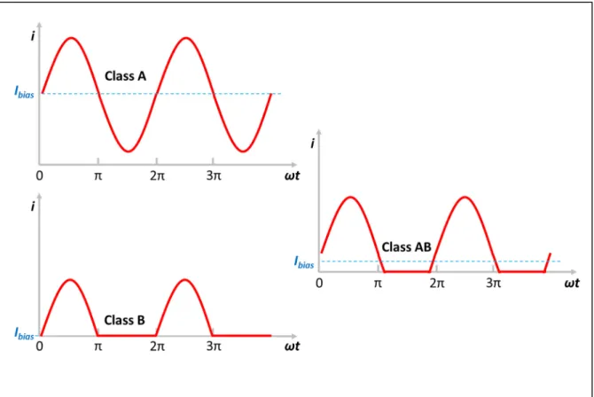
Figure 1.3 Comparison of transient form of the transistor’s drain/collector current under Class A, Class B and Class AB PA operation ...25
Figure 1.4 Implementation of Envelope Tracking PAs ...27
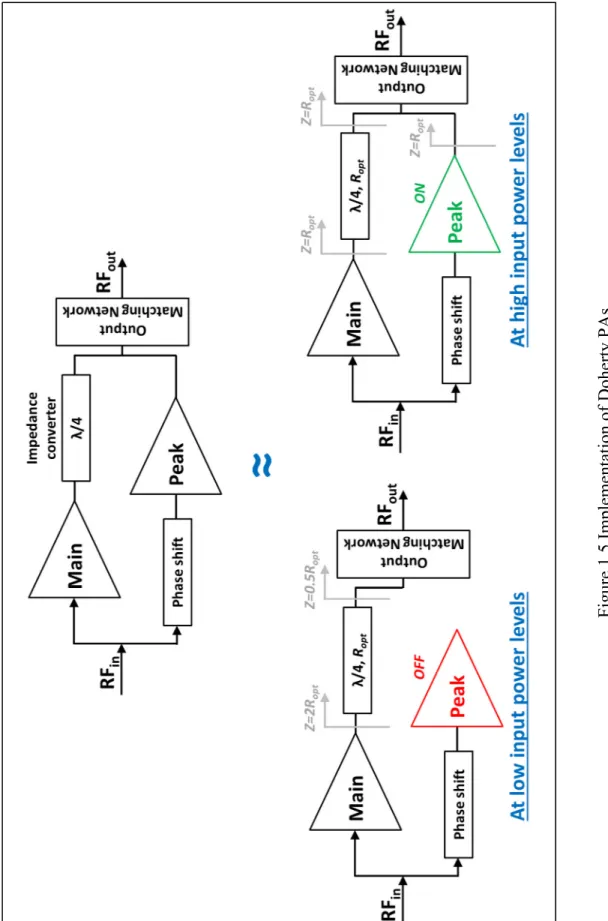
Figure 1.5 Implementation of Doherty PAs ...30
Figure 1.6 Implementation of switching PAs ...33
Figure 1.7 Implementation of dynamic biasing using extensive hardware ...36
Figure 1.8 Implementation of feed-forward envelope-dependent dynamic biasing ...37
Figure 1.9 Schematic of state-of-the-art implementation of negative envelope feedback in RFIC PAs ...40
XXII
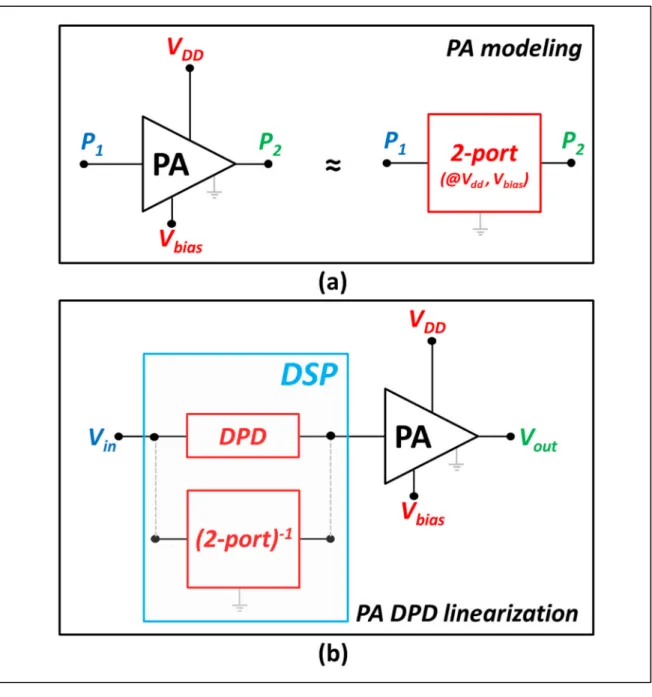
Figure 1.10 Example of a PA design and its equivalent 2-port analytical representation. One possible linearization application using the
analytical representation is also shown ...44 Figure 2.1 Schematic of state-of-the-art multi-stage RFIC PA transmitting an
envelope-modulated signal. VGG=VGG0 refers to the quiescent (DC) gate bias applied to the power-stage transistor array. The PA’s output voltage is clipped for high values of the signal envelope ...56 Figure 2.2 ID vs. VDS profile and the clipped vds waveform when the PA is
excited with the envelope-modulated RF signal vgs. The quiescent (DC) value of the transistor gate voltage is held at VGG0. Q is the PA’s quiescent operating point. vgs and vds are drawn using two different voltage scales ...57 Figure 2.3 Schematic of proposed RFIC PA with positive envelope feedback.
Vdyn is the dynamic-bias signal applied to the gate of the PA’s power-stage transistors. The improvement of the PA’s Gain vs. Pout profile under dynamic bias is also shown, along with the Vdyn vs. Pout profile necessary to achieve it ...58 Figure 2.4 ID vs. VDS profile and the vds waveform for the proposed positive
envelope feedback architecture of Figure 2.3, when the gate is excited with the envelope-modulated RF signal vgs. Q is the PA’s quiescent operating point (identical to the value in Figure 2.2), while
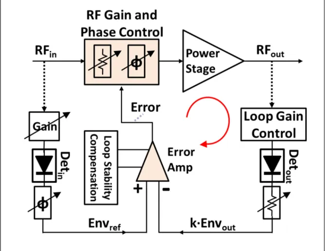
Qdyn is the PA’s instantaneous operating point at high output envelope power levels. Note the reduced clipping of the vds signal compared to that in Figure 2.2. The vds waveform shown is drawn using Qdyn due to the gate voltage value Vdyn corresponding to the maximum envelope level of vgs (in red) ...60 Figure 2.5 Block diagram of PA System with positive feedback loop showing
envelope signal flow ...64 Figure 2.6 Illustration to trace the loop gain of the proposed positive envelope
feedback PA architecture. x, y and z refer to the PA’s power-stage conversion gain from bias input to RF output, the RF-to-analog
conversion gain of the envelope detector and the attenuation through the voltage divider respectively ...65 Figure 2.7 Typical PA power-stage schematic with the time delay tdel from the
gate to the drain of the power-stage cascode transistors. The gate and drain planes are shown with the dotted lines g and d respectively. The group delay ∆ measured over the PA’s signal bandwidth around its carrier frequency frf is also illustrated ...69
XXIII
Figure 2.8 PA with positive envelope feedback showing noise levels at the
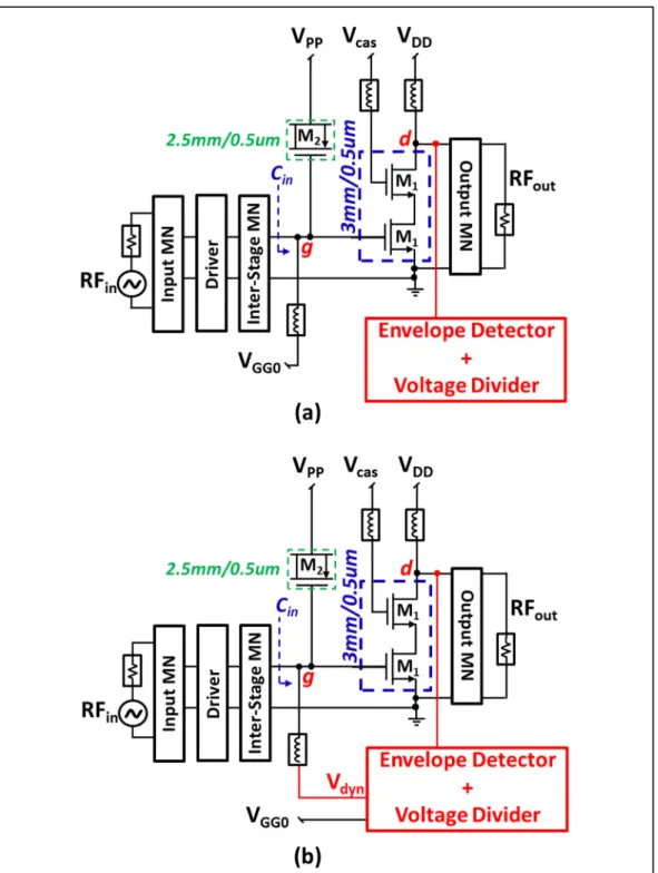
various critical nodes ...70 Figure 3.1 SOI CMOS PA line-up with (a) constant gate bias and (b) dynamic gate
bias through positive envelope feedback. The feedback network is left connected to the output in both cases to avoid using two different output matching networks for (a) and (b) to ensure optimum PA
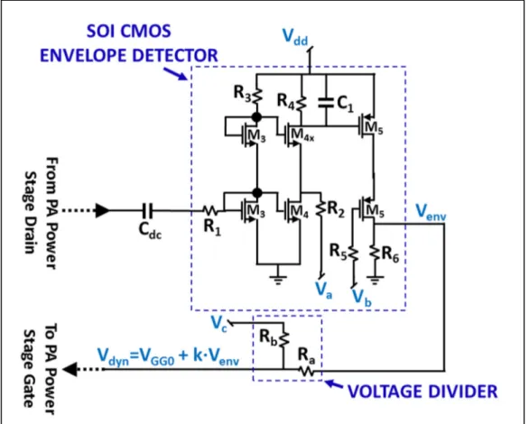
performances ...76 Figure 3.2 Schematic of Envelope Detector and Voltage Divider circuits ...78 Figure 3.3 Vdyn as a function of the average power at the input of the envelope
detector. The detector’s sensitivity (Pref) and the gain conversion slope (ϴ) are indicated, as well as three different profiles of the detector’s transfer function vs. Pout obtained by varying the control voltages Va and Vb. The discontinuities in the plots at low Pout values are simulation artifacts from ADSTM simulation, due to the severe
nonlinearities associated with the detector turn-on and the values of error tolerances used to ensure simulation convergence ...80 Figure 3.4 Gain vs. Pout for PA under 1-tone RF excitation, without and with
positive feedback. The corresponding DC value VGGO of the dynamic-bias signal Vdyn vs. Pout is also shown. An increase in the dynamic gate-bias voltage signal Vdyn at higher output powers linearizes the PA’s Gain profile, while the value of the gate bias at
back-off power levels is kept equal to VGG0 ...83 Figure 3.5 (a) Gain vs. Pout for PA under 2-tone RF excitation, without and with
positive feedback. The frequency spacing used is 1MHz. (b) IMD3 vs. Pout shows an improvement under positive feedback for
Pout>10dBm. Note that the x-axis is the PA’s average Pout ...84 Figure 3.6 IMD3 vs. Pout for PA under 2-tone RF excitation, without and with
positive feedback. The frequency spacing used is 10MHz ...85 Figure 3.7 Transient simulation showing envelope of transistor drain voltage
under two-tone RF excitation, without and with positive envelope feedback. Positive envelope feedback results in reduced clipping. The frequency spacing used is 1MHz and Pout is 16dBm ...86 Figure 3.8 ACPR vs. Pout for PA under modulated RF excitation, without and
with positive feedback. Note that the x-axis is the average Pout ...87 Figure 3.9 Input capacitance Cin seen looking into the PA’s power-stage. Cggn
is the capacitance of the NMOS transistor alone, Cggp is the capacitance of the drain-source shorted PMOS transistor alone and
XXIV
Cggn+Cggp is the total capacitance seen looking into the PA’s power-stage when the NMOS transistor has the gate of the drain-source shorted PMOS transistor connected to its gate ...88 Figure 3.10 Capacitance seen looking into the PA power-stage input as a
function of the PA’s output power, with and without positive envelope feedback. The minimal difference in input capacitance (~80fF) at low output powers is due to the slight loading effect
introduced when the feedback loop is connected ...89 Figure 3.11 Simplified schematic showing PA differential power-stage, envelope
detector and resistive voltage divider in positive envelope feedback
implementation ...93 Figure 3.12 Photograph of prototype dual-IC module shown in Figure 3.11 ...94 Figure 3.13 Gain vs. Pout, Vdyn vs. Pout under CW excitation. The quiescent value
of the Vdyn signal Vdyn(Q), the detector’s sensitivity Pref and the
detector’s gain conversion slope ϴ are also indicated ...94 Figure 3.14 Gain vs. Pout under 2-tone excitation, with constant gate bias and
two different Vdyn profiles (1 and 2) using positive envelope feedback ...95 Figure 3.15 IMD3 vs. Pout under 2-tone excitation, with constant gate bias and
with positive envelope feedback corresponding to “1” in Figure 3.14 ...96 Figure 3.16 PAE vs. Pout under 2-tone excitation, with constant gate bias and with
positive envelope feedback corresponding to “1” in Figure 3.14 ...97 Figure 3.17 (a) Simulated Gain vs. Pout and (b) corresponding IMD3 vs. Pout for
2-tone excitation at 5.4GHz, 10MHz spacing, with the modified design ...99 Figure 3.18 ACPR vs. Pout under modulated excitation, with constant gate bias
and using positive envelope feedback ...100 Figure 3.19 PA output frequency spectrum showing ACP levels under
modulated excitation at Pout=19dBm, with and without positive
envelope feedback ...100 Figure 3.20 Transient Vout voltage signal, with and without positive envelope
feedback, at Pout(average)=19dBm. The corresponding Vdyn signal under positive feedback is also shown and has a maximum swing of ~60mV ...101 Figure 4.1 Proposed embedded self-calibration technique within the mobile
XXV
signal Vctrl is synthesized using X and determines the value of the dynamic-bias signal at different power levels. The input and output probing for self-calibration from unit to unit need to only measure quasi-static input and output power over a narrow power range ...112 Figure 4.2 A second example of the proposed embedded self-calibration
technique within the mobile unit shown in Figure 4.1. The input probe is not required in this implementation, and X instead relies on the baseband chipset within the mobile unit’s processor to
determine the input power to the PA ...113 Figure 4.3 (a) Proposed multi-port analytical representation of PAs under
dynamic bias (b) Equivalent 3-port representation (c) Equivalent 4-port representation ...115 Figure 4.4 PA circuit under multi-tone excitation Vin and with Vctrl=Vdc (under
constant DC supply and biasing). Vo represents the PA’s output multi-tone signal. G is characterized with Vctrl held at Vdc. 1 and 2 are the input and output ports respectively of the 2-port PA
representation ...118 Figure 4.5 2-port PA representation of Figure 4.4 under dynamic bias. Ve is the
dynamic multi-tone component of the bias signal and V’o represents the PA’s new multi-tone output signal. G’ is the new complex
polynomial characterized with the bias node excited by the
dynamic-bias signal Vctrl = Vdc + Ve ...120 Figure 4.6 Proposed 3-port representation of PA under the dynamic biasing
conditions shown in Figure 4.5. Port 3 represents the PA’s bias port.
G is the same complex polynomial in Figure 4.4 characterized with
the PA’s bias node held at Vctrl = Vdc ...121 Figure 4.7 Illustration of the capture of contributions from higher-order PA
nonlinearities using the proposed 3-port representation with the help of lower-order nonlinear polynomials ...124 Figure 4.8 Possible time-domain form of signals at some critical nodes of the
3-port analytical PA representation ...131 Figure 4.9 Equivalent vectorial illustration of signals in the 3-port analytical
PA representation. The red dotted lines in Ve and ∆Va reflect changes in their respective signal amplitudes, and the blue dotted lines reflect changes in their respective signal phases. The possible resulting variations in the PA’s output IMD levels are also shown with coloured spectrum levels of V’o ...133
XXVI
Figure 4.10 Simulated values (solid traces) and predicted values (circular marker traces) of the PA’s output signal, including the output tones at fc-2fx and fc+2fx which are due to the PA’s nonlinearity under quiescent bias. The characterization power level is Pout (avg)
~14dBm ...137 Figure 4.11 Simulated values (solid traces) and predicted values (circular
marker traces) of the PA’s output IMD3 under dynamic bias, at
Pout (avg) ~14dBm ...138 Figure 4.12 Simulated and predicted time-domain form of the PA’s output
envelope signal under dynamic bias with Ve=40mV and Pout (avg) ~14dBm. The time-domain form predicted using only the quasi-static representation is also shown for comparison ...139 Figure 4.13 Implementation of feed-forward dynamic biasing embedded within the
mobile unit for linearization of PA. F is extracted using our 3-port representation X of the PA module, and then applied to the PA module to optimize its output linearity via dynamic biasing ...140 Figure 4.14 PA’s simulated output IMD3 vs. Pout without and with the F block
for dynamic biasing of the PA module ...142 Figure 4.15 PA’s simulated output ACPR vs. Pout without and with the F block
for dynamic biasing of the PA module ...143 Figure 4.16 PA’s simulated output signal (centred at carrier frequency) under
modulated excitation at Pout (avg)~18.3dBm, without and with the F block for dynamic biasing of the PA module ...144 Figure 4.17 Comparison of Gain vs. Pout profile for the original PA and the
new PA examples of Table 4.1 and Table 4.2 ...145 Figure 4.18 Test set-up for experimental validation of proposed 3-port PA
representation ...152 Figure 4.19 Photograph of experimental test set-up shown in Figure 4.18. A
photograph of the SE5003 PA test-board (DUT) is also shown ...153 Figure 4.20 Measured values (dotted markers) and predicted values (solid
traces) of the PA’s IMD3 under dynamic-bias tone Ve. Ve is the Vctrl tone at 𝜔 with the phase kept constant at 80⁰. Other tones are present in Vctrl but are not varied. The PA’s Pout (average) is
29.2dBm ...154 Figure 4.21 Measured values (dotted markers) and predicted values (solid
XXVII
amplitude variation, of its dynamic bias. The PA’s Pout (average) is
29.2dBm ...155 Figure 4.22 (a) Simplified schematic showing closed-loop PA using positive
envelope feedback (b) Prototype system with PA and Envelope
Detector ...160 Figure 4.23 Closed-loop PA under positive feedback, and equivalent open-loop
form using our proposed 3-port PA representation ...162 Figure 4.24 Values of the DUT’s power-stage conversion gain simulated in
ADSTM (black trace) and predicted using the 3-port representation
of (red trace) ...168 Figure 4.25 Measured Gain vs Pout, Vdyn vs Pout with and without positive
envelope feedback ...170 Figure 4.26 Application of proposed 3-port representation for self-calibration
embedded within the mobile unit applied to closed-loop PA under
positive envelope feedback ...172 Figure 4.27 Application of proposed 3-port representation for gain regulation
in PAs that employ ON/OFF transistor matrices ...174 Figure 5.1 Illustration of multi-stage PA design using positive envelope
feedback for dynamic biasing as well as supply modulation, for both the driver-stage and the power-stage transistors. The output of the envelope detector used for positive feedback is also concurrently used for protecting the PA transistors against very large voltage swings arising from VSWR mismatch conditions ...189 Figure 5.2 Illustration of a possible variant of proposed analytical PA
representation to capture PA nonlinearities under simultaneous
dynamic biasing and supply modulation...190 Figure 5.3 Illustration of a possible variant of proposed analytical PA
representation to capture PA nonlinearities under envelope tracking.
I and I’ may capture linear dependencies of the output on the RFin and Envin signals respectively ...191
LIST OF ABBREVIATIONS AND ACRONYMS 3GPP Third Generation Partnership Project
5G-NR Fifth Generation-New Radio ACPR Adjacent Channel Power Ratio AM Amplitude Modulation BJT Bipolar Junction Transistor CAD Computer-Aided Design
CCDF Complementary Cumulative Distribution Function CDMA Code-Division Multiple Access
CG Common Gate
CMOS Complementary Metal-Oxide-Semiconductor
CS Common Source
CW Continuous Wave
DC Direct Current DPD Digital Pre-Distortion DSP Digital Signal Processor DUT Device Under Test
EM Electromagnetic
ET Envelope Tracking
EVM Error Vector Magnitude FET Field-Effect Transistor FM Frequency Modulation GaAs Gallium Arsenide
XXX
HBT Heterojunction Bipolar Transistor
HB Harmonic Balance
IMD Intermodulation Distortion InGaP Indium Gallium Phosphide LCD Liquid Crystal Display LNA Low-Noise Amplifier LTE Long-Term Evolution MCM Multi-Chip Module
ME Mobile Equipment
MMIC Monolithic Microwave Integrated Circuit
MN Matching Network
MOSFET Metal-Oxide-Semiconductor Field-Effect Transistor NMOS Negative-Channel Metal-Oxide Semiconductor
PA Power Amplifier
PAE Power-Added Efficiency PAPR Peak-to-Average Power Ratio PCB Printed Circuit Board
PM Phase Modulation
PMOS Positive-Channel Metal-Oxide Semiconductor PTO Patent and Trademark Office
RF Radio Frequency
RFIC Radio Frequency Integrated Circuit SMT Surface-Mount Technology
XXXI
SOI Silicon-on-Insulator STI Shallow Trench Isolation
UL Uplink
VGA Variable Gain Amplifier VSWR Voltage Standing Wave Ratio
WCDMA Wideband Code Division Multiple Access WLAN Wireless Local Area Network
LIST OF SYMBOLS
β RF-to-analog linear conversion gain of the feedback path λ Wavelength
ω Angular frequency (in radians per second)
A Baseband-to-RF linear conversion gain of the PA’s power-stage Cggn Input capacitance looking into the gate of NMOS transistor
Cggp Input capacitance looking into the gate of PMOS transistor
Cin Input capacitance (e.g. at the input of PA power-stage)
Envin Envelope of input RF signal
f1 Frequency with index 1 (in hertz)
frf RF frequency (in hertz)
ID Drain current
IMD3 Third-order intermodulation distortion product
IMD3hi Upper third-order intermodulation distortion product
IMD5 Fifth-order intermodulation distortion product
P1 Port 1 (e.g. port 1 of a multi-port PA representation)
PDC DC power
Pin Input power level (e.g. at the input of PA)
Pout Output power level (e.g. at the output of PA)
Pref Reference power level (e.g. threshold power level for PA under positive
envelope feedback) Q Quisceint operating point Qdyn Instantaneous operating point
XXXIV
RFdr RF signal at the output of PA driver stage
RFin RF signal at the input of PA (e.g. at the input of PA driver-stage)
RFout RF signal at the output of PA (e.g. at the output of PA power-stage)
Ropt Optimum value of PA output resistance
tdel Absolute value of time delay (e.g. time delay through PA power-stage
transistors)
Tx1 Transmit antenna with index 1
Vbias Bias voltage of PA (e.g. DC bias applied to the gate of PA power-stage)
Vdd Drain supply voltage (e.g. drain supply voltage of PA power-stage in ET PAs)
VDD DC value of drain supply voltage (e.g. DC bias applied to PA power-stage
drain)
vds Drain-source RF voltage signal (in time-domain)
VDS Drain-source DC voltage level
Vdyn Dynamic-bias voltage signal (e.g. envelope-varying bias signal applied to PA
power-stage gate under positive envelope feedback) VGG Gate-bias voltage (e.g. of PA power-stage)
VGG0 Quiescent value of gate-bias voltage (e.g. of PA power-stage)
vgs Gate-source RF voltage signal (in time-domain)
VGS Gate-source DC voltage level
vin Input voltage (e.g. frequency-domain multi-tone voltage signal at PA input)
vin(t) Input voltage in time-domain (e.g. time-domain modulated signal at PA input)
Vin(ωc+iωx) Value of Vin voltage-signal tone at frequency ωc+iωx
vo Output voltage (e.g. frequency-domain multi-tone voltage signal at PA output)
INTRODUCTION
"The mere formulation of a problem is far more often essential than its solution, which may be merely a matter of mathematical or experimental skill. To raise new questions, new possibilities, to regard old problems from a new angle requires creative imagination and marks real advances in science."
Albert Einstein
In this chapter of the thesis, the reader is introduced to the underlying essence of the doctoral research work presented here. The research problems that the work presented in this thesis attempts to find an answer to, as well as the motivation behind trying to solve these problems, are described in Section 0.1. Having presented the research problems, the objectives aimed at through the work reported in this thesis are identified in Section 0.2. In Section 0.3, some of the key contributions that have resulted from this doctoral work are listed while outlining the major theme of each, before presenting their content in greater detail in the subsequent chapters of this thesis.
0.1 Problem statement and motivation
0.1.1 Motivation 1: PAs and the linearity-efficiency trade-off
The power amplifier is a vital component of the RF front-end in mobile units and has always been among the most critical hardware components of the entire RF transmitter, largely determining many of its system performance specifications. Figure 0.1 is a block diagram representation of a typical front-end in an RF transmitter of a mobile device and shows the relative position of the PA (or PAs) within this front-end. As may be observed, the PA inputs interface with the transceiver section (Tx, Rx and Tx-Rx) within the Radio Block (responsible for signal generation, modulation and demodulation) while the PA outputs interface with the transmit antennas (usually via one or more switches) for radio communication with cellular telephony networks or mobile connectivity networks such as Wi-Fi or Bluetooth. The RFIC PA component is therefore responsible for imparting power to
2
(i.e. amplifying) the RF frequency communication signal before being delivered to the antenna and transmitted over the air.
The design of this RFIC PA presents several challenges. Chief among these challenges are optimizing the PA’s efficiency and its linearity, among other critical (and often interrelated) criteria such as bandwidth, gain, noise, silicon area, cost, etc. The PA’s efficiency is commonly measured using the metric Power-Added Efficiency (or PAE) defined by (0.1) below.
𝑃𝐴𝐸 (%) = 𝑃 − 𝑃
𝑃 × 100 (0.1)
where Pout is the PA’s delivered output RF power, Pin is the PA’s input RF power, and PDC is the PA’s DC power that it consumes (e.g. from the battery). As seen by this equation, ideally, the DC power consumed from the battery should be only a little more than the RF power imparted to the transmitted signal by the PA and delivered at its output, for this component to be highly efficient. The PA’s PAE is, therefore, a good measure of its DC power consumption requirements, and a lower efficiency translates into a PA design that is consuming more battery (i.e. DC) power than it should be. The DC power consumed by the PA when it is not transmitting is commonly referred to as the PA’s quiescent power consumption, and a high value of this quiescent power consumption translates into a PA that suffers from poor efficiency. Indeed, a high quiescent power consumption adversely affects the PA’s efficiency not just at lower power levels, but over its entire range of transmitted power levels. The judicious consumption of battery power is critical in mobile devices, where a higher PA efficiency ensures a more extended time period for which the mobile device remains operational before the battery needs to be recharged. While not being the only contributor to the phenomenon, a lower PA efficiency also translates into higher heat production in the mobile device. Such heating issues are because the PA is consuming DC power disproportionate to its requirements, which in turn can negatively affect other PA performances (e.g. gain) as well as make the handheld device uncomfortable to hold.
3
Figure 0.1 Example of typical transmitter architecture of a handheld mobile device showing the use of RFIC PAs. Notice the use of multiple PAs in the transmitter architecture. Each of these PAs have their unique specifications (frequency band of operation, output power, etc.)
and are intended for the transmission of signals targeting different specific applications Adapted from Bailoo (June 2019) and Walsh (September 2010)
4
It is worthwhile to note here that the PA in the mobile device represents approximately 20% of the entire power consumption of a modern cellular device (such as a smartphone) under normal cellular usage conditions (Carroll & Heiser, 2010; Javed, Shahid, Sharif, & Yasmin, 2017). The remainder of the power is shared among other components such as the Liquid Crystal Display (LCD) screen, memory devices, multimedia applications, etc. While this share of the total power consumption by the PA is lower than in older generation cellular devices (since the display, multimedia applications, etc. consumed substantially lower power in these yesteryear devices), it still highlights the significance of the PA’s efficiency in the context of the performance of the entire RF front-end in mobile devices used for cellular communication today.
Having explained the importance of the PA’s efficiency, we now turn our attention to the aspect of the PA’s linearity. The PA’s linearity is a measure of the degree of signal distortion that the PA’s input signal suffers from during amplification through the PA and which is reflected in its delivered output signal, due to the nonlinearities associated with the PA design. Amplification through a power amplifier in a mobile device is an inherently nonlinear process due to several factors intrinsic to semiconductor technology and circuit topology, and which are strongly dependent on the PA voltage supply and PA biasing conditions (i.e. the current intensity applied to the transistors within the PA). Besides linearity, PA biasing is also dictated by considerations regarding efficiency, and all these considerations will be further discussed in Section 1.1. Similar to the metric PAE used for measuring the PA’s efficiency, a number of metrics exist to measure the PA’s degree of nonlinearity, e.g. IMD3,
EVM, ACPR, etc. IMD3 is a simple, popular and useful measurement to perform, and is calculated using a multi-tone (commonly 2-tone or 3-tone) excitation applied to the PA, and measuring the resulting spectrum levels at different frequencies in the PA’s output. For a 2-tone input excitation, if the two input 2-tones are at frequencies f1 and f2=f1+fx, the PA’s output
IMD3 is defined by (0.2).
𝐼𝑀𝐷 = 𝑃 @(𝑓 − 𝑓 )
𝑃 @(𝑓 ) and 𝐼𝑀𝐷 =
𝑃 @(𝑓 + 𝑓 )
5
where IMD3hi and IMD3lo are the upper and lower values of the PA’s third-order intermodulation distortion ratio (IMD3) respectively. Pout @f1-fx refers to the PA’s output spectrum power level at frequency f1-fx; the other definitions of the terms in (0.2) follow likewise. IMD3 values are commonly reported using the decibel scale, which is obtained by taking the ten-base logarithmic value, and then multiplied by 10, of the ratio given in (0.2). Higher-order intermodulation ratios may also be measured. For example, IMD5 ratios are calculated by replacing the numerators in (0.2) with spectral power values at frequencies f1
-2fx and f2+2fx.
A higher value of IMD3 arises from higher values of unwanted distortion products present at the PA output, which itself is a result of a higher degree of PA nonlinearity. These distortion products are present at frequencies other than those used in the excitation signal, i.e. at frequencies f1-fx, f1-2fx, … and f2+fx, f2+2fx …, whereas the input tones are at frequencies f1 and f2 only. PA nonlinearities are undesirable since they result in a transmitted output signal that is a corrupted version of the intended message signal at the PA input and has a direct consequence on the quality of the transmitted signal by the mobile device. Besides, distortion products may fall outside the transmission frequency band and exceed the regulatory out-of-band emission specifications, which are intended to ensure the quality of other communication channels. It is worthwhile to note that PA nonlinearities become especially important at higher output power levels when large-signal effects such as signal clipping come into play.
An ideal PA is, therefore, one which is both efficient and linear over the entire range of power levels that it is transmitting, starting from very low power levels to its maximum rated power level. However, as will be shown in Section 1.1, efficiency and linearity in a PA come at the cost of each other. An extremely linear PA is usually one that suffers from poor efficiency and vice versa. The PA designer, therefore, has to make a choice - a compromise - between the efficiency and the linearity that is desired for any particular PA design, and based on PA specifications tailored to answer the needs of a particular application. This compromise is referred to as the power amplifier’s linearity-efficiency off. The
trade-6
off assumes more considerable significance in the light of modern communication signals, where the complex modulation schemes that are used translate into large peak-to-average power ratios (PAPR) of the signal. The PA transmitting such modulated signals is expected to be both linear and efficient over the entire range of power levels spanned by its average and peak power levels - a challenge that is not trivial to answer.
Improving this linearity-efficiency trade-off is a popular research problem in the field of power amplifiers, and continues to remain an area of active research. A review of popular design strategies that seek to improve this trade-off will also be given in Section 1.1 and highlights the constant evolution and innovation that is a trademark of this area of research. In this thesis also, the fundamental motivation is to improve this linearity-efficiency trade-off in RFIC PAs.
However, through the doctoral studies presented in this thesis, it is sought to answer this research problem while taking into account some additional constraints. These additional constraints stem from the need for circuit simplicity – and the advantages that any PA performance improvement technique offers when it is simple. The simpler a PA technique is, the more feasible it is to realize it as a standalone integrated RFIC PA solution or to incorporate it into (and operate in conjunction with) already existing PA architectures. The main characteristics of such simple techniques are: the requirement of minimum additional chip area, the consumption of minimum additional power and the necessity of minimum additional signal processing. Such attributes are especially attractive in the context of millimetre-wave PAs envisaged for 5G applications, where it is believed that given the large bandwidths, complex constellations and large PAPR of the signals that are envisioned for deployment, digital techniques alone cannot satisfy all the requirements to guarantee efficient and linear PA operation (P. M. Asbeck, Rostomyan, Özen, Rabet, & Jayamon, 2019). Both digital and analog techniques have to be used concurrently to meet all the needs of such PAs, and the simplicity of the analog technique will be critical in determining its feasibility for integrating into the RFIC front-end module of the transmitter.
7
Having explained the research motivation, which will be alluded to throughout the rest of this document and especially in Chapter 2 and Chapter 3, we may now state our first problem statement as given in Section 0.1.2.
0.1.2 Problem Statement 1
There is a need for power amplifier circuit techniques that improve the PA’s linearity-power efficiency trade-off while remaining simple - i.e. requiring minimum additional chip area, minimum additional power and no external signal processing. A PA circuit technique that would meet these requirements facilitates its realization as an integrated RFIC PA solution, as well as contributes to its feasibility for incorporation into existing RFIC PA architectures. 0.1.3 Motivation 2: PAs and part-to-part variation
A second source of research motivation for the work presented in this thesis is related to the variation of PA performance from part-to-part in different mobile units, and a need for an automatic self-calibration method that allows achieving optimum PA performances across parts. This aspect is now explained in the succeeding paragraphs.
PA integrated circuits are designed with the help of Computer-Aided Design (CAD) software tools, using circuit models that reflect the typical performance parameters of various devices. For example, the MOSFET performance parameters (transconductance, noise, etc.) simulated by the PA designer during a CMOS SOI PA design process generally reflects its typical values. They are simulated under different circuit conditions (e.g. biasing, temperature, etc.) that can be varied within the CAD simulator. During a first design cycle, the designer optimizes a PA design based on these simulated typical values given by the circuit models.
In reality, however, device performances may vary considerably across parts in different mobile units due to many factors, e.g. semiconductor manufacturing process variations, inconsistencies in assembly, deviations in the encapsulation used, etc. Additionally, these
8
variations are also aggravated as the complexity of the PA design increases, e.g. PAs that use hardware reconfiguration, envelope-dependent control mechanisms, dynamic biasing, etc. In such cases, process variations of the required additional circuitry (e.g. switches in PAs that use hardware reconfiguration, envelope detectors in envelope-controlled PAs, biasing circuitry in dynamic-bias PAs, etc.) add to the already significant performance variations of the basic PA line-up. These are also further accentuated by differences in the biasing and other circuit conditions (e.g. temperature) from one mobile device to another.
As a result, the PA performances simulated using the typical circuit models do not reflect the measured performances that may be expected from the actual fabricated PA circuit. While modern simulators allow the designer to predict in advance (to a certain degree) what these variations will be, it is extremely difficult to design a PA that achieves its best possible performance across all these variations from part-to-part. Subsequent PA design cycles after the first rely on data gathered through extensive measurements in the laboratory over many different PA parts which are deliberately taken from different process corners of the wafer. These measured values are then correlated with the typical simulated values, to select the best value of different PA circuit parameters – common for all the parts of a particular PA design in a given production run – which ensures a satisfactory yield of PA parts that meet the range of performance limits fixed in the target specifications.
The common PA circuit parameter values that are ultimately selected through circuit adjustments at the prototyping stage for any given PA design, therefore, represent a
compromise: they ensure that all the delivered PA parts meet the limits of performance
variation fixed in the target specifications despite the deviation in their performance from one PA part to another, even though the common circuit parameter values do not allow all the PA parts to achieve their best possible individual performance in the mobile device. Such a compromise has implications for both the PA manufacturer as well as the Mobile Equipment (ME) manufacturer. The PA manufacturer is forced to relax the guaranteed limits related to the PA design’s performance in the specifications datasheet, to account for all the part-to-part variations of performances compared to that of the typical PA part. Such a relaxation is
9
necessary to increase PA yield from any given fabrication run. The ME manufacturer faces a similar conundrum arising from PA performance variations due to inconsistencies in the PA assembly within the mobile unit. Such inconsistencies for the ME manufacturer may occur due to a number of factors – e.g. due to deviations from manufacturing tolerances in the PCBs that are used, variations in the bias voltage and supply voltage sources, irregularities in the wire-bonding, etc.
To better explain this, refer to Figure 0.2, which is a portion of the datasheet of a commercial RFIC PA design (SKY85402-11 [Datasheet], August 2018). As can be seen, most performance metrics are associated with a higher and a lower limiting value specified by the PA manufacturer. These limiting values reflect the extremities of the spread in performance that may be expected due to variation from one PA part to another. Such a spread, though undesired, is difficult to circumvent and is accounted for as part of the tolerable limits of performance deviation that is deemed acceptable for a given PA design.
In this context, an automatic self-calibration technique that enables PA performance optimization from one part to another during operation of the mobile equipment would be of interest to any stakeholder in the mobile industry associated with RFIC PAs, and significantly affect the design and operating strategies adopted by RFIC PA manufacturers and ME manufacturers for current and future mobile wireless equipment. The manufacturer may also perform a first calibration step during production/assembly; subsequent automatic self-calibration is performed in the field during operation of the mobile equipment.
Such a calibration technique would target enhancing PA performances within the mobile equipment by ensuring close-to-optimum performance across parts, by varying one or more key circuit parameters from part-to-part in different mobile units during operation. To allow embedding within the mobile equipment, the calibration should be performed with simple (and minimum) probing circuitry and require a simple calibration training sequence based on a minimal number of measurements. The aforementioned is what we refer to as embedded
10
performance across PA parts and enable the PA manufacturer to guarantee more aggressive specifications by ensuring that a higher number of PA parts are operating at close to optimum performance. In turn, this will positively affect the time-to-market of the mobile equipment and potentially help in securing the edge over the competition. It will be further shown in Section 1.3 and Chapter 4 that the analytical PA representation for PA performance characterization proposed in this thesis may significantly contribute towards the realization of such an embedded self-calibration technique. An example where self-calibration would be useful is when the PA is subjected to dynamic biasing through the modulation of the gate bias as a function of the PA’s envelope, to improve its linearity-efficiency trade-off. Embedded self-calibration would then allow performing the necessary adjustments on the dynamic bias applied to each PA part to reduce the spread in performance from one mobile unit to another, hence ensuring close-to-optimum PAE-linearity trade-off in every mobile unit.
Having explained this second research motivation, which will be reiterated in Chapter 4, we may now state our second problem statement as given in Section 0.1.4.
0.1.4 Problem Statement 2
There is a need for a method of power amplifier self-calibration that enables automatic optimization of PA performance across parts, from one mobile equipment to another. Such a method would allow each PA part in different mobile equipment to achieve close-to-optimum performance. To allow such a self-calibration method to be embedded within the mobile unit, it should use simple probing circuitry and require a simple training sequence based on only a minimum number of measurements.
0.2 Research objectives
With our research motivation clearly explained in Section 0.1, the objectives of the doctoral research work presented in this thesis are as follows:
11
Figure 0.2 E
xcerpt from a typical PA da
tasheet showing different
specifications. The typical
value, the upper limit
and the lowe
r limit of th
e guaranteed
values of these different perform
ance specificatio
ns are also s
hown
Taken from
SKY85402-11 Da
12
• To propose and demonstrate a new method of power amplifier design to improve the linearity-efficiency trade-off in RFIC PAs and which requires minimum additional overhead for implementation, i.e. minimum additional chip area, minimum additional power consumption and no external signal processing.
• To propose and demonstrate a multi-port analytical representation of PAs for the processing of the input modulated RF signal and any envelope-dependent dynamic biasing signal, and which facilitates accomplishing the research objective stated in the third bullet point below.
• To propose and demonstrate a method of self-calibration of PAs that is embedded within the mobile unit and based on the proposed multi-port analytical PA representation of the second bullet point above, for automatic performance optimization of open-loop and closed-loop PAs from one mobile unit to another.
0.3 Research contributions
The first investigations within the broader framework of my research work were started in Fall 2013, when I embarked on my Master’s studies at ÉTS as part of an M.A.Sc.-Ph.D. integrated program, having been awarded the “ÉTS Excellence awards for international students – Master’s-PhD Award.” Besides completing the requisite courses, the research conducted during this period resulted in two publications. This work also formed the basis of some of the more theoretical aspects of my doctoral studies. The contributions are listed below, along with a brief description summarizing their content:
Sharma, S., & Constantin, N. G. (December 2013). Formulations for the Estimation of IMD Levels in an Envelope Feedback RFIC Amplifier: An Extension to Dynamic AM and PM Behavior. IEEE Transactions on Computer-Aided Design of Integrated Circuits
13
• The aforementioned paper extends Professor Constantin’s previously published work for estimating PA IMD levels, by additionally accounting for PA nonlinearities arising from memory effects, with the help of novel formulations that describe a system of complex nonlinear equations. The intended application is for estimating the linearity requirements of circuit blocks typically found in the error signal paths of envelope feedback amplifiers, to facilitate the design and test of RFIC PAs within a computer-aided IMD test setup.
Sharma, S., & Constantin, N. (May 2014). An Algorithm for IMD Computation in Automated
Tests of RFIC Power Amplifiers. Paper presented at the 2014 IEEE Canadian
Conference on Electrical and Computer Engineering (CCECE).
• The above paper presents an algorithm for the computation of IMD levels in RFIC PAs. The algorithm is aimed at overcoming typically encountered convergence problems when solving systems of nonlinear equations associated with PA behavioural models. The algorithm is intended to facilitate the implementation of these behavioural models as part of a computer-aided IMD test setup.
Following this, I undertook a research internship at Skyworks Solutions, Inc., Ottawa. The focus of this internship was aligned along the axis of my first research problem stated in Section 0.1.2. As part of this work, I investigated, measured and performed design work on a complex industrial SOI CMOS PA platform. Various aspects of this work included examining techniques related to PA gate capacitance linearization, PA linearization, PA protection under Voltage Standing Wave Ratio (VSWR) mismatch, etc. Much of the original work stemming from the research started during this period, and then continued after, relate to a novel concept that I have introduced during the course of my Ph.D. research: positive envelope feedback, applied to RFIC PAs and that form the crux of the material presented in Chapter 2 and Chapter 3 of this thesis. The resulting research contributions are enumerated below:
Sharma, S., & Constantin, N. G. (January 2017). Amplifier architecture using positive envelope feedback. United States Patent Application no 10,320,345