HAL Id: hal-02525210
https://hal-ip-paris.archives-ouvertes.fr/hal-02525210
Submitted on 30 Mar 2020
HAL is a multi-disciplinary open access
archive for the deposit and dissemination of
sci-entific research documents, whether they are
pub-lished or not. The documents may come from
teaching and research institutions in France or
abroad, or from public or private research centers.
L’archive ouverte pluridisciplinaire HAL, est
destinée au dépôt et à la diffusion de documents
scientifiques de niveau recherche, publiés ou non,
émanant des établissements d’enseignement et de
recherche français ou étrangers, des laboratoires
publics ou privés.
Rydberg excitons in Cu 2 O microcrystals grown on a
silicon platform
Stephan Steinhauer, Marijn Versteegh, Samuel Gyger, Ali Elshaari, Birgit
Kunert, André Mysyrowicz, Val Zwiller
To cite this version:
Stephan Steinhauer, Marijn Versteegh, Samuel Gyger, Ali Elshaari, Birgit Kunert, et al.. Rydberg
excitons in Cu 2 O microcrystals grown on a silicon platform. Communications Materials, 2020, 1,
pp.11. �10.1038/s43246-020-0013-6�. �hal-02525210�
Rydberg excitons in Cu
2
O microcrystals grown on a
silicon platform
Stephan Steinhauer
1✉
, Marijn A.M. Versteegh
1, Samuel Gyger
1, Ali W. Elshaari
1, Birgit Kunert
2,
André Mysyrowicz
3& Val Zwiller
1Cuprous oxide (Cu2O) is a semiconductor with large exciton binding energy and significant
technological importance in applications such as photovoltaics and solar water splitting. It is also a superior material system for quantum optics that enabled the observation of intriguing phenomena, such as Rydberg excitons as solid-state analogue to highly-excited atomic states. Previous experiments related to excitonic properties focused on natural bulk crystals due to major difficulties in growing high-quality synthetic samples. Here, the growth of Cu2O
microcrystals with excellent optical material quality and very low point defect levels is pre-sented. A scalable thermal oxidation process is used that is ideally suited for integration on silicon, demonstrated by on-chip waveguide-coupled Cu2O microcrystals. Moreover, Rydberg
excitons in site-controlled Cu2O microstructures are shown, relevant for applications in
quantum photonics. This work paves the way for the wide-spread use of Cu2O in
optoe-lectronics and for the development of novel device technologies.
https://doi.org/10.1038/s43246-020-0013-6 OPEN
1Department of Applied Physics, KTH Royal Institute of Technology, SE-106 91 Stockholm, Sweden.2Institute of Solid State Physics, Graz University of
Technology, A-8010 Graz, Austria.3Laboratoire d’Optique Appliquée, ENSTA, CNRS, Ecole Polytechnique, F-91762 Palaiseau, France. ✉email:[email protected]
123456789
L
ight-matter interactions in the direct-band-gap semi-conductor cuprous oxide (Cu2O) are widely governed byexcitons, quasi-particles arising from electron-hole Coulomb interactions, which can be observed up to room temperature due to their large binding energy. As a result of the unique excitonic properties, intriguing condensed-matter quantum phenomena have been demonstrated, e.g. spectroscopic signatures of quantum-degenerate exciton gases1,2 as well as giant Rydberg excitons3 exhibiting signatures of quantum coherences4 and
quantum chaotic behavior5. As the exciton ground state– the
so-called paraexciton – is decoupled from the radiation field in unstrained Cu2O, paraexcitons can reach lifetimes up to
micro-seconds6 rendering them a prime candidate for excitonic
Bose-Einstein condensation7. Apart from quantum optics, recent reports have reinforced the significant potential of Cu2O as a
low-cost, non-toxic material in areas such as photocatalysis8, solar
water splitting9, and solar cell devices10 showing promising
photovoltaic efficiencies and marked excitonic effects11. Various
methods have been reported for the growth of Cu2O thin films
and single crystals12, in particular molecular beam epitaxy13,14,
magnetron sputtering15,16in combination with thermal anneal-ing17, electrodeposition18, thermal oxidation19, and thefloating
zone method20. However, state-of-the-art quantum optics
experiments still focus on natural bulk crystals originating from mines, clearly underlining that significant progress in Cu2O
growth is required to surpass inherent limitations of natural samples. Recent literature emphasized that for the observation of Rydberg states with principal quantum numbers higher than the current record value of n= 25 samples with lower impurity concentrations are required21. In addition, scalable fabrication
techniques suitable for obtaining micro-/nanostructures and compatible with standard silicon processing are needed to deploy the full potential of this material in advanced device technologies, for instance integrated quantum photonic circuits.
In this work, we present Cu2O growth by a scalable thermal
oxidation process, which resulted in microcrystal structures with very low point defect and impurity levels. Our method offers the opportunity for combining high-quality Cu2O with silicon-based
integrated photonics, which we demonstrate by on-chip coupling of exciton luminescence to a silicon nitride waveguide. In single Cu2O microcrystals studied at cryogenic temperatures under
continuous-wave excitation we demonstrate luminescence from excited np Rydberg states in lithographically site-controlled structures, exhibiting excellent agreement with a hydrogen-like quantum number dependence. Due to the exceptional optical material quality and the unique excitonic properties, our Cu2O
microcrystals are highly promising for enabling new integrated photonic device architectures relevant for quantum information processing and quantum sensing.
Results and discussion
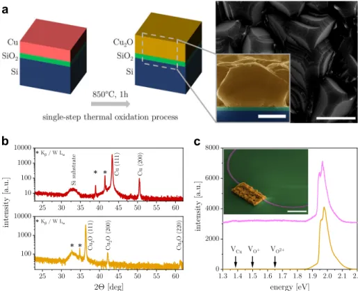
Growth and photoluminescence properties. The growth of Cu2O microcrystals relied on a scalable single-step thermal
oxi-dation process schematically depicted in Fig. 1a. Copper films (thickness ~700 nm) were deposited by electron beam evapora-tion on silicon substrates covered with a thermal SiO2 layer.
Thermal oxidation in a tube furnace resulted in Cu2Ofilms with
microcrystalline morphology, which can be seen in the top-view and cross-sectional scanning electron microscopy images. The Cu2O microcrystals showed terrace-like structures on the surface
(Supplementary Fig. 1) and faceted grains with sizes in the μm range. As-deposited copper and samples after thermal oxidation to Cu2O were characterized by X-ray diffraction (XRD)
mea-surements (Fig.1b) to determine their phase composition. For as-deposited copper, the expected face-centered cubic structure and
texturing along the [111] direction was found. The presented single-step thermal oxidation method resulted in phase-pure Cu2O with cubic cuprite structure. For samples fabricated with
different growth conditions comparable microcrystal morphology as well as similar XRD results were obtained (Supplementary Fig. 2).
Thermal oxidation of copper can lead to different oxide phases12; Cu2O growth was reported to proceed via the random
nucleation of islands, which exhibit a cube-on-cube epitaxial relationship at the metal-oxide interface (low oxygen partial pressures)22or non-epitaxial orientations (above critical oxygen partial pressures depending on the copper surface)23. For the
range of experimental parameters corresponding to the growth conditions used in this study (800–850 °C, p ~1 mbar of synthetic air) the initial stages of copper oxidation include epitaxial oxide formation accompanied by rapid two-dimensional growth24. The
XRD results before and after thermal oxidation (Fig. 1b) show pronounced texturing in {111} direction in both cases, indicating that the oxidation proceeds via an epitaxial relationship of Cu2O {111}∥ Cu {111}. This relationship is in accordance with
literature reports on the thermal oxidation of copper thinfilms22 and nanoparticles with sizes down to few nanometers25. Similar
to a previous report on epitaxial Cu2O growth on MgO15, the
observed terrace-like structures on the Cu2O surfaces are
suggesting a two-dimensional growth mode for individual microcrystals.
In addition to growth on planar silicon substrates covered with thermal SiO2, we show the integration of Cu2O microcrystals with
pre-patterned silicon nitride waveguides (see Methods section). Site-controlled microstructures were obtained by thermal oxida-tion of lithographically defined copper rectangles (length 20 μm, width 10μm) using the same parameters as described above. The optical material quality was assessed by means of room-temperature photoluminescence spectroscopy of Cu2O grown
on both planar substrates and on waveguide structures. In the latter case, waveguide-coupled Cu2O luminescence was collected
from the cleaved silicon nitride side facet (see experimental setup in Supplementary Fig. 3). Distinct free exciton emission was observed (Fig. 1c) for both types of samples, exhibiting a characteristic lineshape resulting from multiple phonon-assisted recombination processes with spectral overlap13. At photon
energies attributed to copper vacancies or single/double-charged oxygen vacancies12 no marked luminescence was observed.
Additional data for microcrystalline Cu2O films from different
batches and grown under different conditions can be found in Supplementary Fig. 4, which shows spectra with very similar characteristics. Hence, the presented single-step thermal oxida-tion process is a robust method for the realizaoxida-tion of microcrystalline Cu2O films with very low point defect levels,
ideally suited for the on-chip integration with waveguide structures. Compared to previous literature reports on Cu2O
growth on silicon (e.g. refs. 16–18), our results demonstrate a
unique combination of excellent optical material quality, site-controlled growth and suitability for photonic circuit integration, which holds great promise for enabling integrated devices with novel functionalities based on excitons in Cu2O. In the following,
we will focus on photoluminescence spectroscopy of single Cu2O
microcrystals at milli-Kelvin temperatures to probe their funda-mental excitonic properties.
Point defects and yellow 1s excitons. Local deviations from the ideal cuprite crystalline structure, e.g. vacancy point defects, extrinsic impurities or microscopic strain, have a significant impact on the relaxation of excitons in Cu2O and the related
photon emission. Low point defect densities are highly important
for efficient cooling of the exciton gas in Cu2O as trapping at
defects is a limiting factor for exciton lifetimes. The latter were found to be significantly shortened for increasing oxygen vacancy concentrations26. Furthermore, it has been suggested that
relaxation processes involving vacancies can lead to heating due to phonon emission27, which is detrimental for achieving cold
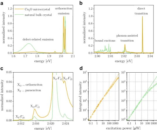
exciton gas temperatures. Photoluminescence spectroscopy experiments were conducted in a dilution refrigerator (sample stage base temperature around 40 mK) to assess the optical material quality of Cu2O microcrystals at milli-Kelvin
tempera-tures. The results were compared to natural bulk Cu2O as
benchmark (crystal originates from a selected high-quality geo-logical sample used in previous literature1,2,6). Spectra normalized
to the yellow 1s orthoexciton emission that were acquired at a laser power of 50μW (corresponding to a peak intensity of 3 kW cm−2) and an excitation wavelength of 532 nm are pre-sented in Fig.2a, showing considerably reduced emission related to oxygen vacancies for the case of Cu2O microcrystals. An
emission feature around 1.95 eV was observed for both Cu2O
microcrystals and the natural bulk sample, which has been reported repeatedly in literature. It was attributed to phonon-assisted transitions and defect emission in close spectral proximity14,27,28with the latter potentially being correlated with
local strain in the sample29. The ratio of excitonic over defect emission for the measurements shown in Fig.2a was found to be aboutfive times higher for the Cu2O microcrystals compared to
the bulk sample. Additional data for different samples and natural bulk crystal positions as well as further discussion can be found in Supplementary Fig. 5. In addition to intrinsic point defects,
excitons and their luminescence properties may be influenced by the presence of extrinsic impurities. The latter can lead to the formation of bound excitons, which show multiple emission lines in the energy range around ~2.00 eV, below the phonon-assisted orthoexciton transition30. In Fig.2b, we directly compare pho-toluminescence spectra obtained from synthetic Cu2O
micro-crystals and from the natural bulk crystal under identical experimental conditions (excitation power 50 nW). It is evident that all peak-like features related to excitons bound to extrinsic impurities are absent in Cu2O microcrystals, once more
validat-ing the excellent purity and material quality of our samples. Moreover, we assess the energy level structure of yellow 1s exci-tons in Cu2O microcrystals by monitoring luminescence from
different phonon-assisted transitions (Fig. 2c). The emission features were assigned according to previous literature31and the energy splitting of 1s excitons into orthoexcitons and para-excitons separated by 12 meV in unstrained Cu2O was validated.
The influence of strain on the luminescence spectra of Cu2O
microcrystals is discussed in Supplementary Fig. 6.
Exciton relaxation was further studied by assessing its excitation power dependence. For this purpose, the incident laser power was varied and the luminescence spectra were integrated in an energy range covering bound excitons, phonon-assisted transitions and the direct quadrupole line (Fig. 2d). The integrated intensity of the Cu2O microcrystal is in excellent
agreement with a linear relationship (slope 0.995 ± 0.008) for excitation powers spanning more than two orders of magnitude, showing slight sub-linear behavior at elevated excitation levels. On the other hand, deviations from a linear power dependence
Fig. 1 Growth and characterization of Cu2O microcrystals. a Schematics of sample layer structure before and after the thermal oxidation process (left).
Top-view scanning electron micrograph of Cu2O microcrystals after thermal oxidation at 850∘C for 1 h at pressures of 1 mbar synthetic air (right); the
bottom inset shows a corresponding cross-sectional image (scale bars 1μm). b X-ray diffraction of as-deposited copper film (top) and Cu2Ofilm after
thermal oxidation (bottom).c Room-temperature photoluminescence spectroscopy of Cu2O microcrystals under continuous-wave laser excitation
(532 nm). Emission from free exciton recombination around 2 eV was observed from Cu2O microcrystals in continuousfilms on SiO2(bottom orange line).
Further, Cu2O microstructures were grown on silicon nitride waveguides (device configuration shown in the inset; scale bar 10 μm) and on-chip coupling
were significantly more pronounced for the natural bulk crystal. Sub-linear power dependence of excitonic emissions in Cu2O has
been previously observed in experiments using natural bulk samples30,32,33and synthetic crystals grown by thefloating zone
method34 using various types of laser excitation. It has been attributed to an efficient non-radiative two-body recombination process, which can be explained by Auger decay35, by the
formation of short-lived biexcitons36or by exciton
interconver-sion via spin exchange37. The estimated recombination rates reported in literature vary considerably as the process is expected to be sensitive to Cu2O crystal symmetry and the resulting band
structure; hence it has been anticipated that Auger recombination is associated with broken band symmetries in the vicinity of impurities7, which would explain the less pronounced two-body
decay in low-defect-density Cu2O microcrystals.
Rydberg excitons of the yellow np series. After initial experi-ments in the middle of the last century, Rydberg excitons in Cu2O
have recently attracted considerable attention due to the experi-mental demonstration of principal quantum numbers up to n= 25 in absorption measurements using natural bulk crystals3.
For synthetic Cu2O films in the thickness range of few
micro-meters and below, Rydberg excitons up to n= 4 have been found38,39. Previous studies on natural bulk Cu
2O crystals
indi-cated that under above-band excitation Rydberg excitons are generated via collision processes of 1s excitons28,40. The question
arises if Rydberg states can also be observed in the Cu2O
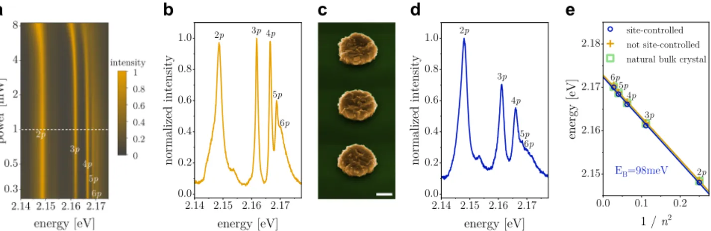
microcrystals presented here, which was assessed by means of
photoluminescence experiments. Results obtained for varying incident laser powers are presented in Fig.3a (spectra normalized to their respective maxima). Emission peaks corresponding to Rydberg excitons up to n= 6 were identified at intermediate excitation, which can also be seen in the exemplary spectrum shown in Fig. 3b. The 2p peak showed a markedly asymmetric lineshape consistent with previous literature on bulk Cu2O
crystals28,40,41, whereas the relative emission intensities from np
states differed in our case. The minor peak between the 2p and 3p energy level is attributed to 1s excitons of the green series28.
Rydberg exciton emission showed broadening for increasing excitation power, which can be explained by a combination of phonon scattering and density-dependent effects40; the red shift
indicates a bandgap decrease due to laser-induced sample heating. Most importantly, the power-dependent measurements verify the robustness of Rydberg excitons in Cu2O microcrystals as their
emission was detected in a wide range of excitation conditions. To reduce the line broadening, measurements were performed at considerably lower excitation powers. The spectral overlap of states with higher quantum numbers could be reduced and the observation of Rydberg excitons with n= 7 was possible, which is further detailed in Supplementary Fig. 7 and the related discus-sion. Additional photoluminescence spectroscopy data from dif-ferent samples is shown in Supplementary Fig. 8, validating that Rydberg excitons can be consistently observed in Cu2O
microcrystals.
Furthermore, site-controlled Cu2O microstructures (Fig. 3c)
were achieved by lithographic patterning of the copper film before oxidation. We demonstrate luminescence from excited
Fig. 2 Photoluminescence spectroscopy of Cu2O microcrystals at milli-Kelvin temperatures benchmarked to measurements on a natural bulk crystal.
a Normalized photoluminescence of excitons and point defects (excitation power 50μW). b Normalized emission from different excitonic transitions and bound excitons at low excitation power of 50 nW.c Phonon-assisted transitions of ortho- and paraexcitons (spectra normalized to direct transition; excitation power 50μW). d Excitation power dependence of integrated emission in an energy range covering bound excitons, phonon-assisted transitions and the direct quadrupole line. Solid lines are a linearfit (Cu2O microcrystal, left) and a linear curve as guide to the eye (natural bulk crystal, right),
respectively.
Rydberg states in a circular Cu2O microstructure with 5μm
diameter (Fig.3d). The intensity ratio of np states was different compared to Cu2O microcrystals, which could be explained by
variations in microscopic strain41. The Rydberg exciton energies were evaluated as a function of n−2for results obtained from site-controlled microstructures, from not site-site-controlled microcrystals and from a natural bulk crystal (Fig. 3e). Excellent agreement with a linear relation was found and exciton binding energies of 98 meV and 97 meV were deduced for the synthetic samples and the natural bulk crystal, respectively. The extracted exciton binding energies concur with previous findings using bulk crystals, obtained from both photoluminescence (97 meV40;
98.5 meV41) and absorption measurements (98 meV42). Hence
our results demonstrate the realization of site-controlled, micrometer-sized Cu2O structures as host platform for Rydberg
excitons, which goes beyond the state of the art of Cu2O growth
on silicon and opens up opportunities for unprecedented photonic device architectures. For instance, our technology will enable applications in nonlinear quantum optics relying on interactions between Rydberg states43, as clear signatures of the Rydberg blockade effect have been recently reported for principal quantum numbers around n= 621. To observe Rydberg states
with higher principal quantum number n, it will be promising to explore Cu2O microcrystals with larger size as well as different
excitation schemes that mitigate luminescence broadening40and
the potential influence of free carriers induced by above-band excitation21.
In summary, we have presented the growth of Cu2O
microcrystals showing excellent optical material quality with very low point defect and impurity levels, combined with the integration on a silicon platform including the on-chip coupling to silicon nitride waveguide structures. The fabrication method for obtaining high-quality Cu2O films via a scalable thermal
oxidation process has guiding significance for diverse areas where this low-cost, non-toxic material is employed, such as photo-voltaics and photocatalysis. Furthermore, the demonstration of Rydberg excitons in Cu2O microcrystals and their integration on
silicon have far-reaching implications for future applications in photonic quantum information processing. For instance, Rydberg states in Cu2O have been proposed for the realization of novel
solid-state single-photon sources44 and giant optical
nonlinea-rities45. Hence our work lays the foundation for a platform
technology enabling solid-state Rydberg excitations on-chip,
which is envisioned to result in integrated devices capable of generating and manipulating light at the single-photon level.
Methods
Growth of Cu2O microcrystals on silicon substrates. The deposition of copper
films (thickness ~700 nm) was performed by electron beam evaporation onto pieces of silicon wafers with 150 nm thermal SiO2. A thin intermediate titanium
layer (thickness ~5 nm) was employed to improve thefilm adhesion on the sub-strate surface. Samples with structured Cu2O were realized by patterning the
copperfilm using an electron beam lithography lift-off process. Thermal oxidation was carried out in a tube furnace connected to a vacuum pump. Before growth experiments the system was evacuated and purged multiple times using high-purity synthetic air (Air Liquide Alphagaz 2). Cu2O samples were grown by thermal
oxidation at a pressure around 1 mbar and setpoint temperatures of 800 °C or 850 ° C. The temperature was kept constant for 1 h or 5 h after reaching the setpoint value, followed by natural sample cool-down.
Sample characterization. The morphologies of Cu2Ofilms and microstructures
were characterized by scanning electron microscopy imaging of the sample surfaces and of cross-sections obtained by mechanical cleaving. X-ray diffraction mea-surements were performed by specular scans using a PANalytical Empyrean sys-tem. Radiation from a sealed copper tube was used in combination with a secondary graphite monochromator in Bragg-Brentano geometry. Phase analysis was carried out relying on powder patterns from the database PDF2, International Center for Diffraction Data, using 004-0836 for Cu and 005-0667 for Cu2O.
Photoluminescence spectroscopy. All photoluminescence spectroscopy experi-ments were performed using a Horiba iHR550 spectrometer and a continuous-wave, diode-pumped solid-state laser emitting at 532 nm. Room-temperature spectra were acquired using an objective (NA= 0.82) for excitation and collection. Spectroscopy at milli-Kelvin temperatures was performed relying on a cryogen-free dilution refrigerator (Bluefors) with a base temperature around 10 mK. Optical side-access windows with anti-reflective coatings were used for laser excitation of the samples mounted on a dedicated stage controlled by piezoelectric actuators, which had a base temperature around 40 mK. The laser was focused by a lens (NA= 0.50) inside the cryostat to a spot diameter around 1.2μm (full width at half maximum); the power was measured at the outermost cryostat window.
Waveguide integration of Cu2O microstructures. Commercial silicon wafers
covered with 3.3μm wet thermal oxide and 335 nm of stoichiometric silicon nitride deposited by low-pressure chemical vapor deposition were used as substrates. Waveguides with a width of 1 μm were fabricated using electron beam lithography and reactive ion etching using CHF3/CF4/O2gas chemistry. Integrated Cu2O
microstructures were realized by an electron beam lithography lift-off process and thermal oxidation at 850 °C for 1 h. Photoluminescence spectroscopy of the waveguide-integrated device was performed using an Acton SpectraPro spectro-meter with 750 mm focal length, excitation normal to the sample surface (con-tinuous-wave 532 nm laser) through an objective (NA= 0.28) and collection from the cleaved waveguide facet using another objective (NA= 0.65).
Fig. 3 Rydberg excitons in Cu2O microcrystals and site-controlled structures. a Normalized photoluminescence ofnp Rydberg exciton emission from
Cu2O microcrystal for varying excitation powers. The white dashed line indicates the spectrum presented inb which was acquired at an excitation power of
1 mW and a cryostat stage temperature around 1.8 K.c Scanning electron micrograph of site-controlled circular Cu2O microstructures with 5μm diameter
(scale bar 2μm; sample tilt 45°). d Photoluminescence spectrum of site-controlled Cu2O microstructure that was acquired under identical experimental
Data availability
The data that support thefindings of this study are available from the corresponding author upon reasonable request.
Received: 13 December 2019; Accepted: 10 February 2020;
References
1. Snoke, D., Wolfe, J. P. & Mysyrowicz, A. Quantum saturation of a Bose gas: excitons in Cu2O. Phys. Rev. Lett. 59, 827–830 (1987).
2. Snoke, D. W., Wolfe, J. P. & Mysyrowicz, A. Evidence for Bose-Einstein condensation of a two-component exciton gas. Phys. Rev. Lett. 64, 2543–2546 (1990).
3. Kazimierczuk, T., Fröhlich, D., Scheel, S., Stolz, H. & Bayer, M. Giant Rydberg excitons in the copper oxide Cu2O. Nature 514, 343–347 (2014).
4. Grünwald, P. et al. Signatures of quantum coherences in Rydberg excitons. Phys. Rev. Lett. 117, 133003 (2016).
5. Aßmann, M., Thewes, J., Fröhlich, D. & Bayer, M. Quantum chaos and breaking of all anti-unitary symmetries in Rydberg excitons. Nat. Mater. 15, 741–745 (2016).
6. Mysyrowicz, A., Hulin, D. & Antonetti, A. Long exciton lifetime in Cu2O.
Phys. Rev. Lett. 43, 1123–1126 (1979).
7. Snoke, D. & Kavoulakis, G. M. Bose-Einstein condensation of excitons in Cu2O: progress over 30 years. Rep. Prog. Phys. 77, 116501 (2014).
8. Wu, S.-C., Tan, C.-S. & Huang, M. H. Strong facet effects on interfacial charge transfer revealed through the examination of photocatalytic activities of various Cu2O-ZnO heterostructures. Adv. Funct. Mater. 27, 1604635
(2017).
9. Pan, L. et al. Boosting the performance of Cu2O photocathodes for unassisted
solar water splitting devices. Nat. Catal. 1, 412–420 (2018).
10. Minami, T., Nishi, Y. & Miyata, T. Efficiency enhancement using a Zn1−xGex
-O thinfilm as an n-type window layer in Cu2O-based heterojunction solar
cells. Appl. Phys. Express 9, 052301 (2016).
11. Omelchenko, S. T., Tolstova, Y., Atwater, H. A. & Lewis, N. S. Excitonic effects in emerging photovoltaic materials: a case study in Cu2O. ACS Energy Lett. 2,
431–437 (2017).
12. Meyer, B. K. et al. Binary copper oxide semiconductors: from materials towards devices. Phys. Stat. Sol. (B) 249, 1487–1509 (2012).
13. Li, J. et al. Engineering of optically defect free Cu2O enabling exciton
luminescence at room temperature. Opt. Mater. Express 3, 2072–2077 (2013). 14. Kracht, M., Schörmann, J. & Eickhoff, M. Plasma assisted molecular beam
epitaxy of Cu2O on MgO(001): influence of copper flux on epitaxial
orientation. J. Cryst. Growth 436, 87–91 (2016).
15. Yin, Z. G. et al. Two-dimensional growth of continuous Cu2O thinfilms by
magnetron sputtering. Appl. Phys. Lett. 86, 061901 (2005). 16. Park, J.-W. et al. Microstructure, optical property, and electronic
band structure of cuprous oxide thinfilms. J. Appl. Phys. 110, 103503 (2011).
17. Bergum, K. et al. Improving carrier transport in Cu2O thinfilms by rapid
thermal annealing. J. Phys. Condens. Matter 30, 075702 (2018). 18. Oba, F. et al. Epitaxial growth of cuprous oxide electrodeposited onto
semiconductor and metal substrates. J. Am. Ceram. Soc. 88, 253–270 (2005). 19. Mani, S., Jang, J., Ketterson, J. & Park, H. High-quality Cu2O crystals with
various morphologies grown by thermal oxidation. J. Cryst. Growth 311, 3549–3552 (2009).
20. Chang, K. B., Frazer, L., Schwartz, J. J., Ketterson, J. B. & Poeppelmeier, K. R. Removal of copper vacancies in cuprous oxide single crystals grown by the floating zone method. Cryst. Growth Des. 13, 4914–4922 (2013). 21. Heckötter, J. et al. Rydberg excitons in the presence of an ultralow-density
electron-hole plasma. Phys. Rev. Lett. 121, 097401 (2018).
22. Zhou, G. et al. In situ atomic-scale visualization of oxide islanding during oxidation of Cu surfaces. Chem. Commun. 49, 10862–10864 (2013). 23. Luo, L., Kang, Y., Yang, J. C. & Zhou, G. Effect of oxygen gas pressure on
orientations of Cu2O nuclei during the initial oxidation of Cu(100), (110) and
(111). Surf. Sci. 606, 1790–1797 (2012).
24. Gattinoni, C. & Michaelides, A. Atomistic details of oxide surfaces and surface oxidation: the example of copper and its oxides. Surf. Sci. Rep. 70, 424–447 (2015).
25. LaGrow, A. P., Ward, M. R., Lloyd, D. C., Gai, P. L. & Boyes, E. D. Visualizing the Cu/Cu2O interface transition in nanoparticles with environmental
scanning transmission electron microscopy. J. Am. Chem. Soc. 139, 179–185 (2017).
26. Koirala, S., Naka, N. & Tanaka, K. Correlated lifetimes of free paraexcitons and excitons trapped at oxygen vacancies in cuprous oxide. J. Lumin. 134, 524–527 (2013).
27. Frazer, L., Chang, K. B., Schaller, R. D., Poeppelmeier, K. R. & Ketterson, J. B. Vacancy relaxation in cuprous oxide (Cu2−xO1−y). J. Lumin. 183, 281–290 (2017).
28. Takahata, M. & Naka, N. Photoluminescence properties of the entire excitonic series in Cu2O. Phys. Rev. B 98, 195205 (2018).
29. Frazer, L. et al. Evaluation of defects in cuprous oxide through exciton luminescence imaging. J. Lumin. 159, 294–302 (2015).
30. Jang, J. I., Sun, Y., Watkins, B. & Ketterson, J. B. Bound excitons in Cu2O:
Efficient internal free exciton detector. Phys. Rev. B 74, 235204 (2006). 31. Mysyrowicz, A., Trauernicht, D. P., Wolfe, J. P. & Trebin, H. R. Stress
dependence of the paraexciton in Cu2O. Phys. Rev. B 27, 2562–2564 (1983).
32. O’Hara, K. E., Gullingsrud, J. R. & Wolfe, J. P. Auger decay of excitons in Cu2O. Phys. Rev. B 60, 10872–10885 (1999).
33. Stolz, H. et al. Condensation of excitons in Cu2O at ultracold temperatures:
experiment and theory. New J. Phys. 14, 105007 (2012).
34. Karpinska, K., Mostovoy, M., van der Vegte, M. A., Revcolevschi, A. & van Loosdrecht, P. H. M. Decay and coherence of two-photon excited yellow orthoexcitons in Cu2O. Phys. Rev. B 72, 155201 (2005).
35. Wolfe, J. P. & Jang, J. I. The search for Bose-Einstein condensation of excitons in Cu2O: exciton-Auger recombination versus biexciton formation. New J.
Phys. 16, 123048 (2014).
36. Jang, J. I. & Wolfe, J. P. Auger recombination and biexcitons in Cu2O: A case
for dark excitonic matter. Phys. Rev. B 74, 045211 (2006).
37. Kavoulakis, G. M. & Mysyrowicz, A. Auger decay, spin exchange, and their connection to Bose-Einstein condensation of excitons in Cu2O. Phys. Rev. B
61, 16619–16622 (2000).
38. Naka, N., Hashimoto, S. & Ishihara, T. Thinfilms of single-crystal cuprous oxide grown from the melt. Jpn J. Appl. Phys. 44, 5096–5101 (2005). 39. Takahata, M., Tanaka, K. & Naka, N. Nonlocal optical response of
weakly confined excitons in Cu2O mesoscopicfilms. Phys. Rev. B 97, 205305
(2018).
40. Kitamura, T., Takahata, M. & Naka, N. Quantum number dependence of the photoluminescence broadening of excitonic Rydberg states in cuprous oxide. J. Lumin. 192, 808–813 (2017).
41. Reimann, K. & Syassen, K. Raman scattering and photoluminescence in Cu2O
under hydrostatic pressure. Phys. Rev. B 39, 11113–11119 (1989). 42. Matsumoto, H., Saito, K., Hasuo, M., Kono, S. & Nagasawa, N. Revived
interest on yellow-exciton series in Cu2O: an experimental aspect. Solid State
Commun. 97, 125–129 (1996).
43. Firstenberg, O., Adams, C. S. & Hofferberth, S. Nonlinear quantum optics mediated by Rydberg interactions. J. Phys. B At. Mol. Opt. Phys. 49, 152003 (2016).
44. Khazali, M., Heshami, K. & Simon, C. Single-photon source based on Rydberg exciton blockade. J. Phys. B At. Mol. Opt. Phys. 50, 215301 (2017). 45. Walther, V., Johne, R. & Pohl, T. Giant optical nonlinearities from Rydberg
excitons in semiconductor microcavities. Nat. Commun. 9, 1309 (2018).
Acknowledgements
We thank Roland Resel for helpful discussions. The Quantum Nano Photonics Group at KTH acknowledgesfinancial support from the Linnaeus Center in Advanced Optics and Photonics (ADOPT). S.S. acknowledges funding from the Swedish Research Council under grant agreement No. 2019-04821. M.A.M.V. acknowledges funding from the Swedish Research Council under grant agreement No. 2016-04527. S.G. acknowledges funding from the Swedish Research Council under grant agreement No. 2016-06122 (Optical Quantum Sensing). A.W.E. acknowledges funding from the Swedish Research Council Starting Grant (2016-03905) and from a Marie Skłodowska-Curie Individual Fellowship under REA grant agreement No. 749971 (HyQuIP). V.Z. acknowledges funding by the European Research Council under grant agreement No. 307687 (NaQuOp), the Swedish Research Council under grant agreement No. 638-2013-7152 and the Göran Gustafsson Foundation. The project was co-funded by Vinnova and FP7 (GROWTH 291795). Open access funding provided by Royal Institute of Technology.
Author contributions
S.S., M.A.M.V., and V.Z. conceived the experiments, with input from A.M. M.A.M.V. designed and built the milli-Kelvin photoluminescence spectroscopy setup. S.S. per-formed material growth, SEM characterization and photoluminescence experiments. S.G. and A.W.E. fabricated and characterized waveguide-integrated structures. Data analysis and interpretation was performed by S.S. with support from M.A.M.V., A.M., and V.Z. XRD characterization and the corresponding analysis was performed by B.K. The project was supervised by M.A.M.V. and V.Z. The manuscript was written by S.S. with inputs from all authors.
Competing interests
The authors declare no competing interests.
Additional information
Supplementary informationis available for this paper at https://doi.org/10.1038/s43246-020-0013-6.
Correspondenceand requests for materials should be addressed to S.S.
Reprints and permission informationis available athttp://www.nature.com/reprints
Publisher’s note Springer Nature remains neutral with regard to jurisdictional claims in published maps and institutional affiliations.
Open Access This article is licensed under a Creative Commons Attribution 4.0 International License, which permits use, sharing, adaptation, distribution and reproduction in any medium or format, as long as you give appropriate credit to the original author(s) and the source, provide a link to the Creative Commons license, and indicate if changes were made. The images or other third party material in this article are included in the article’s Creative Commons license, unless indicated otherwise in a credit line to the material. If material is not included in the article’s Creative Commons license and your intended use is not permitted by statutory regulation or exceeds the permitted use, you will need to obtain permission directly from the copyright holder. To view a copy of this license, visithttp://creativecommons.org/ licenses/by/4.0/.