HAL Id: hal-02383437
https://hal.archives-ouvertes.fr/hal-02383437
Submitted on 27 Nov 2019
HAL is a multi-disciplinary open access
archive for the deposit and dissemination of
sci-entific research documents, whether they are
pub-lished or not. The documents may come from
teaching and research institutions in France or
abroad, or from public or private research centers.
L’archive ouverte pluridisciplinaire HAL, est
destinée au dépôt et à la diffusion de documents
scientifiques de niveau recherche, publiés ou non,
émanant des établissements d’enseignement et de
recherche français ou étrangers, des laboratoires
publics ou privés.
MIS STRUCTURES FOR SOLAR CELLS
PERIMETER PASSIVATION
Amaury Delamarre, Hassanet Sodabanlu, Kentaroh Watanabe, Masakazu
Sugiyama, Jean-Francois Guillemoles
To cite this version:
Amaury Delamarre, Hassanet Sodabanlu, Kentaroh Watanabe, Masakazu Sugiyama, Jean-Francois
Guillemoles. MIS STRUCTURES FOR SOLAR CELLS PERIMETER PASSIVATION. 36th
EU-PVSEC, Sep 2019, Marseille, France. �hal-02383437�
MIS STRUCTURES FOR SOLAR CELLS PERIMETER PASSIVATION
Amaury Delamarre1,2,*, Hassanet Sodabanlu1,3, Kentaroh Watanabe1,3, Masakazu Sugiyama1,3, Jean-François
Guillemoles1,4
1NextPV, Tokyo 153-8904, Japan; 2Centre for Nanoscience and Nanotechnology, CNRS, University
Paris-Sud/Paris-Saclay, 91120 Palaiseau, France; 3Research Center for Advanced Science and Technology, The University of Tokyo,
Tokyo 153-8904, Japan; 4Institut Photovoltaïque d’Ile-de-France (IPVF), 91120 Palaiseau, France
ABSTRACT: Perimeter recombination takes place in all photovoltaic architectures, its detrimental effect increasing with the perimeter to area ratio. A new efficient passivation method is introduced here, inspired by the working principle of MOSFETs. It consists in a Metal Insulator stack, deposited on top of the Semiconductor structure. As a transistor, it acts as a switch to prevent the flow of majority carriers towards the defective side walls. Simulation results show that the detrimental effect of perimeter recombination can be reduced by half in the particular case of a GaAs solar cell under one sun illumination. Because no chemical treatment is involved, our MIS based passivation solution can be adapted to various photovoltaic materials as a perspective. A possible additional application will be devices working under intense illumination, where resistive effects are a limiting factor.
Keywords: III-V Semiconductors, Concentrator Cells, Gallium Arsenide Based cells, Passivation
1 INTRODUCTION
Perimeter recombination is a mechanism occurring in any photovoltaic technology, its influence increasing while the cell area is reduced. Microscale solar cells can be found for various applications, such as concentrated photovoltaics, laser power converter or distributed energy harvesters [1]–[3]. The purpose of this communication is to introduce a new original and efficient passivation method, that does not use any chemical treatment. Instead, our strategy is to modulate the conductivity of the lateral spreading layers. This is done with a Metal Insulator Semiconductor (MIS) stack, deposited on the top of the cell, along its perimeter [4]. Its working principle is inspired from MOSFETs transistors, as introduced in the second section.
Although the MIS passivation strategy could be adapted to different materials, we will focus in this communication on GaAs solar cells. Firstly, because it is a widespread material, used in various microscale application. Secondly because open surfaces of GaAs are particularly recombinative [5]. Despite chemical passivation treatments exist (e.g. [6], [7]), perimeter recombinations are identified as one of the limiting factors in various configurations [2], [3], [8].
2 BASIC PRINCIPLE
The basic principle of the MIS passivation method can be introduced with the structure in Figure 1. It consists in a MIS stack deposited on top of the cell, along its perimeter. Similarly to a MOSFET transistor, applying a voltage to the gate electrode will generate a depletion layer in the window and emitter layers of the device. This has the effect of increasing the resistivity of those lateral current spreading layers, hence preventing the majority carrier current flow towards the recombinative surface. 2 SIMULATION RESULTS AND DISCUSSION
The structure presented in Figure 1 has been simulated with the Sentaurus software. It consists in a circular solar cell, with a 220 µm radius. Such a cell area is comparable to microcells considered for various applications, such as distributed light harvester or CPV [3], [8]. The area considered for the efficiency
estimations includes the area covered by the front contact and the gate electrode, so that shadowing losses are accounted. The circular geometry is selected for simulation convenience, but other geometry can be equally considered. The light generation is obtained with a monochromatic illumination at 532 nm. The incident intensity is set at 65.2 mW/cm², so that the obtained short circuit is 27.3 mA/cm², a value comparable to reported GaAs solar cell performances under 1 sun. The cell efficiencies given in the following will therefore be estimated as a ratio of the power delivered by the device and an incident illumination of 100 mW/cm². Only radiative recombinations are considered in the bulk. Recombination are introduced at the perimeter of the device, so that the associated saturation current is 1.5e-12 A/cm, with an ideality factor of 2, consistent with values reported in the literature [8], [9]. The gate voltage is given as the voltage difference between the gate electrode and the front contact electrode.
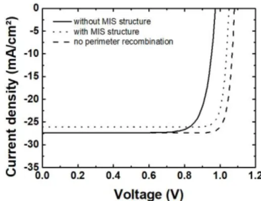
The simulated J(V) curves are plotted in Figure 2, for three different cases. Firstly, an ideal case is considered, with no recombination at the perimeter, resulting VOC =
1.08 V, JSC = 27.4 mA/cm² and FF= 88.7 %, so that the
efficiency is 26.3 %. This configuration represents the upper limit of perfect perimeter passivation. In a second case, the perimeter recombination is introduced, resulting in a severe VOC reduction to 0.97 V and FF to 81.4 %, the
cell efficiency being reduced by an absolute 4.7 %. Finally, the gate structure is included, with an applied gate voltage Vgate = -3 V. Both the VOC and the FF are
partially recovered, respectively to 1.05 V and 87.8 %. The short circuit current is slightly reduced to 26.1 mA/cm², due to an increased shadowing owing to the gate electrode. Nevertheless, an efficiency improvement of an absolute 2.4 % is observed, representing roughly half the losses introduced by the perimeter recombination.
36th European Photovoltaic Solar Energy Conference and Exhibition
Figure 1 Simulated structure with the Sentaurus software. The cell is circular, with a 220 µm radius. The red dashed boxes schematically represent the depletion layer generated in the window and the emitter layers by a voltage applied at the gate electrode. Those depletion layers prevent lateral currents towards the side walls.
Figure 2 Simulated J(V) curves for the cell structure in Figure 1. For (solid line) a sample without the gate structure, and (dotted line) with a gate structure and Vgate
= -3 V. The dashed line represents a simulation in which no perimeter recombination is included.
In order to illustrate the working principle of the modulated lateral resistivity, the energy band diagrams are plotted along the depth of the device, at the gate coordinate, in Figure 3 (a) and (b), respectively for a sample without and a sample with the gate structure. The voltage difference between the back and the front contact is set at 1.15 V, the voltage difference between the gate electrode and the front electrode is -3 V. In (a), a band diagram similar to usual solar cells is obtained. In (b) the voltage applied to the gate electrode bends the bands upwards, resulting in a depletion of the window and the emitter layer. This has the effect of increasing the lateral resistances, preventing the electron current flow towards the recombinative perimeter.
It should be noted that the space charge region width at the pn junction is reduced for increasing forward voltage bias. As a result, the conductivity of the emitter is increased with increased forward voltage, so that the enhanced resistivity obtained thanks to the gate structure becomes less pronounced.
Figure 3 Band diagram along the depth of the sample, (a) for a sample without the gate structure, and (b) for a sample with the gate structure at Vgate = –3 V.
The graphs in Figure 3 also highlight the main limitation of the MIS passivation strategy. In order to obtain an efficient resistivity increase in the window / emitter stack, it is necessary to generate a depletion width as large as possible. This limits the compatible window / emitter thickness and doping, i.e. their conductivity. Under one sun, the thickness and doping combination presented in Figure 1 is found compatible with negligible series resistance effect and efficient perimeter passivation by the MIS structure.
4 PERSPECTIVES
The MIS based passivation method introduced in this communication does not involve any chemical treatment of the defective surface itself, as is done in usual passivation methods. Consequently, this method can be applied to any solar cell design, as long as a lateral current spreading layer is included.
An additional original application will be solar cells under concentration. With increased illumination intensity, a cell efficiency is increased, until series resistance losses appear due to large current densities, reducing the fill factor. An optimum concentration is obtained as a consequence. The series resistances have different origins, some of them being related to lateral currents, such as the emitter and window sheet resistances, and the metal contact finger resistances. The impact of those lateral resistances can be drastically reduced by reducing the cell area [10]–[12]. This strategy is however limited by perimeter recombinations, which increase with the perimeter to area ratio, and which we can precisely reduce with the MIS passivation method introduced here. Using it on devices operated under
36th European Photovoltaic Solar Energy Conference and Exhibition
concentration can help reducing the cell size, increasing the optimum illumination, thereby increasing their efficiencies.
5 CONCLUSION
A new perimeter passivation method is introduced in this study, its basic principle relying on modulating the window / emitter sheet resistances. This is achieved by depositing a MIS structure on the top of the cell, with which a depletion layer can be generated in the top layers of the cell. This principle is inspired by the working principle of MOSFETs transistors.
Particularly, a GaAs microcell (220 µm diameter) has been simulated by Sentaurus, under an illumination comparable to 1 sun. Compared to an ideal case where no perimeter recombinations are considered, the efficiency loss introduced by those recombinations is estimated at an absolute 4.7 %. Thanks to the introduced MIS passivation structure, this efficiency loss is reduced to 2.3%.
As a perspective, the introduced passivation method can be considered for other material or cell architectures, as well as under concentrated illumination.
6 REFERENCES
[1] B. Gai, J. F. Geisz, D. J. Friedman, H. Chen, and J. Yoon, “Printed assemblies of microscale triple‐junction inverted metamorphic GaInP/GaAs/InGaAs solar cells,” Prog. Photovolt.
Res. Appl., p. pip.3127, Mar. 2019.
[2] R. Kimovec, H. Helmers, A. W. Bett, and M. Topič, “Comprehensive electrical loss analysis of monolithic interconnected multi-segment laser power converters,” Prog. Photovolt. Res. Appl., vol. 27, no. 3, pp. 199–209, Mar. 2019.
[3] E. Moon, I. Lee, D. Blaauw, and J. D. Phillips, “High‐efficiency photovoltaic modules on a chip for millimeter‐scale energy harvesting,” Prog. Photovolt. Res. Appl., vol. 27, no. 6, pp. 540–546,
Jun. 2019.
[4] J. F. Guillemoles and A. Delamarre, “Semiconductor Device with Structure for Passivating Recombining Surfaces,” WO2019158430, 22-Aug-2019.
[5] L. J. Brillson, “Metals on Semiconductors,” in
Surfaces and interfaces of electronic materials,
Weinheim: Wiley-VCH, 2010, pp. 447–522. [6] E. Yablonovitch, C. J. Sandroff, R. Bhat, and T.
Gmitter, “Nearly ideal electronic properties of sulfide coated GaAs surfaces,” Appl. Phys. Lett., vol. 51, no. 6, p. 439, 1987.
[7] M. T. Sheldon, C. N. Eisler, and H. A. Atwater, “GaAs Passivation with Trioctylphosphine Sulfide for Enhanced Solar Cell Efficiency and Durability,”
Adv. Energy Mater., vol. 2, no. 3, pp. 339–344,
Mar. 2012.
[8] P. Espinet-González, I. Rey-Stolle, M. Ochoa, C. Algora, I. García, and E. Barrigón, “Analysis of perimeter recombination in the subcells of GaInP/GaAs/Ge triple-junction solar cells,” Prog.
Photovolt. Res. Appl., vol. 23, no. 7, pp. 874–882,
Jul. 2015.
[9] H. Xu et al., “Current transport efficiency analysis of multijunction solar cells by luminescence imaging,” Prog. Photovolt. Res. Appl., Jul. 2019.
[10] C. Algora and V. Diaz, “Design and optimization of very high power density monochromatic GaAs photovoltaic cells,” Electron Devices IEEE Trans.
On, vol. 45, no. 9, pp. 2047–2054, 1998.
[11] M. Paire et al., “Microscale solar cells for high concentration on polycrystalline Cu(In,Ga)Se2 thin films,” Appl. Phys. Lett., vol. 98, no. 26, p. 264102, 2011.
[12] A. Vossier, B. Hirsch, E. A. Katz, and J. M. Gordon, “On the ultra-miniaturization of concentrator solar cells,” Sol. Energy Mater. Sol.
Cells, vol. 95, no. 4, pp. 1188–1192, Apr. 2011.
36th European Photovoltaic Solar Energy Conference and Exhibition