UNIVERSITÉ DU QUÉBEC
INRS - ÉNERGIE MATÉRIAUX TÉLÉCOMMUNICATIONS
Subcycle nonlinear terahertz optics:
a carrier dynamics approach
By
Xin Chai
A thesis submitted in partial fulfillment of the requirements for the degree of
Doctor of Philosophy (PhD) in Energy and Material Sciences
Jury Members
President of the jury Dr. Luca Razzari (INRS-EMT)
& Internal examiner
External examiner Dr. Lyubov Titova (Worcester Polytechnic Institute)
Dr. Jean-Michel Ménard (University of Ottawa)
Acknowledgement
I am first and foremost grateful to my research advisor, Professor Tsuneyuki Ozaki. I was extremely lucky to have an exceptional and furthermore, a super cool research director. During my PhD, I have been struggling to solve certain problems and it really took some time. However, he always trusted me with the freedom to pursue challenging projects and gave me the resources to see them through to completion. In this he taught me to become an independent researcher. The discussions with Prof. Ozaki were always encouraging, interesting and fruitful. Moreover, Prof. Ozaki has provided me with many opportunities of potential collaborations, international conferences as well as my future career.
I would sincerely like to thank my colleague Dr. Xavier Ropagnol for his support during my PhD. It is his expertise on the large-aperture photoconductive antenna terahertz source that makes this dissertation even possible. He was always there to ask and working closely with him has truly been a pleasure.
I am very thankful to my former colleague Dr. Hassan. A. Hafez for his great help, especially during the first two years of my PhD. He was always inspiring and motivating me.
I’m grateful to Dr. Muhammad Ashiq Fareed, who is super nice and intelligent. He helped us a lot on improving the quality of our manuscript.
I would also like to thank the technical team of ALLS: Philippe Lassonde and Antoine Laramée for their huge help on maintaining and aligning the laser facilities. Nothing will come out with a bad laser.
I am also very grateful to Prof. Savel’ev’s group from Lomonosov Moscow State University for their tremendous effort on the DSTMS THz source.
I would also like to thank Prof. Richard Martel and Prof. Pierre Lévesque for the collaboration and providing the gated graphene samples.
I’m also very thankful to Prof. François Blanchard for his help on improving our THz experimental setup and his trust on me for modelling some of his experimental results.
I would also like to thank the NTT group: Prof. Hiroki Hibino, Dr. Yoshiaki Sekine, Dr. Katsuya Oguri and Dr. Makoto Takamura for their collaboration and supplying graphene samples.
I’m extremely grateful for Prof. Marc Dignam and Prof. David Cooke for the fruitful discussions we had on graphene and on the initial results of In0.53Ga0.47As.
I’m also very grateful for my colleagues Denis Ferachou, Marie Kirouac-Turmel, Sudipta Mondal, Fatemeh Amirkhan, Luis Sanchez-Mora, Singh Mangaljit, Isgandarov Elchin, Carlos. M. Garcia-Rosas for their help and collaboration.
Great thanks to the members of the jury: Prof. Luca Razzari, Prof. Lyubov Titova and Prof. Jean-Michel Ménard for reviewing and evaluating my thesis.
In the end, I would like to thank my family and my friends for everything. It has been a wonderful journey and I’m pretty sure that everything will become better and better.
Abstract
The dynamics of free electrons in semiconductors play the central role in strong light-matter interaction with intense terahertz radiations. Terahertz pulse can serve as a transient voltage bias to drive high-field phenomena in solids. Various nonlinear effects can be excited by applying different terahertz field strengths and the observed experimental results are found to be extremely sensitive to the incident terahertz spectrum and its temporal profile. These properties suggest a rich variety of possible optoelectronic applications by controlling the carrier dynamics in semiconductors.
In this thesis, we investigate the nonlinear terahertz responses of free charge carriers in semiconductors, such as the n-doped semiconductor In0.53Ga0.47As and graphene, with terahertz time-domain spectroscopy as well as optical pump-terahertz probe spectroscopy. We start by discussing the terahertz responses of monolayer graphene. Then we discuss the significant impact of temporal dynamics in subcycle nonlinear optics. There are several limitations of the conventional Drude model and more importantly, the experimental observations may differ significantly within the well-known THz window. Strong subcycle nonlinear optics can only be achieved by carefully taking into account the time-scale of the variation in the temporal conductivity. Different experimental results are observed using different coherent terahertz sources in the frequency range between 0.1 and 3 THz. To retrieve nonlinear optics in the subcycle regime, we performed nonlinear THz-TDS on a common doped semiconductor material In0.53Ga0.47As, which possesses a much higher carrier density and a high conductivity contrast before and after strong carrier heating induced by intervalley scattering. Our findings suggest an incoherent
approach to subcycle control of terahertz high-frequency (or high-harmonic) generation based on intraband carrier scattering effects. These investigations will be important for future terahertz electronics and optoelectronics.
Table of Contents
Acknowledgement ... i
Abstract ... iii
Chapter 1. Introduction ... 1
Chapter 2. Nonlinear time-resolved terahertz spectroscopy ... 3
2.1 Photoconductive antenna terahertz source ...4
2.2 Optical rectification ...8
2.3 Electro-optic sampling technique ... 12
2.4 Terahertz time-domain spectroscopy ... 16
2.5 Optical-pump terahertz-probe spectroscopy ... 19
Chapter 3. Terahertz spectroscopy of graphene... 21
3.1 Terahertz electrodynamics of graphene ... 21
3.2 Ambient temperature effects on the carrier dynamics in graphene ... 23
3.3 Nonlinear terahertz time-domain spectroscopy of gated graphene ... 29
Chapter 4. Nonlinear terahertz optics induced by intraband carrier dynamics ... 33
4.1 Nonlinear THz intraband conductivity ... 33
4.2 Intuition of subcycle nonlinear THz optics induced by carrier scattering ... 36
4.3 Ensemble Monte-Carlo approach ... 40
Chapter 5. Subcycle nonlinear terahertz optics ... 46
5.1 Half-cycle nonlinear terahertz optics ... 47
5.2 Adding another half-cycle pulse with opposite polarity ... 53
5.3 Terahertz Harmonic generation due to intervalley scattering effect (theory) ... 62
Chapter 6. From intraband to interband nonlinear terahertz optics ... 66
6.1 Observation from intraband to interband carrier dynamics ... 67
Chapter 7. From linear to circular ponderomotive acceleration ... 77
7.1 Generation of elliptically polarized terahertz pulses ... 78
7.2 Elliptically polarized THz-TDS on In0.53Ga0.47As ... 79
7.3 Development of detection approach using Stokes-Mueller formalism ... 81
Chapter 8. Conclusions and Perspectives ... 91
List of Figures
Fig.2.1: Schematic diagram of the THz generation from a photoconductive antenna. A bias voltage Vb is applied on the semiconductor substrate to drive the photoexcitation carriers. ... 4
Fig.2.2: A photo of the iLAPCA source (without binary mask) developed at ALLS. ... 6
Fig.2.3: THz pulses generated from a ZnSe based iLAPCA THz source. The inset shows the corresponding spectrum. Here, the long negative half-cycle is cut at 6.4 ps due to the overlap with the back reflected pulses from the detection crystal, substrate of the studied sample and the antenna substrate. ... 7
Fig.2.4: Schematic diagram of the THz generation by using titled-pulse-front technique in a LiNbO3 crystal. ... 10
Fig.2.5: Quasi-single-cycle THz pulses generated from a LiNbO3 crystal via OR. The inset shows the corresponding spectrum. ... 11
Fig.2.6: (a) Schematic diagram of the THz detection system using EO sampling technique. (b) A femtosecond laser pulse serves as an ultrafast detector to scan the THz waveforms. ... 12
Fig.2.7: Schematic diagram of a THz-TDS set-up. ... 16
Fig.2.8: Normal incidence and transmission of THz electric field through a thin conducting film deposited on a dielectric substrate: (a) substrate - thin film configuration and (b) thin film – substrate configuration, where another Fresnel loss at the substrate-air interface should be taken into account for the measured field by EO sampling. ... 17
Fig.2.9: (a) Schematic diagram of an optical/IR-pump THz-probe system (b) Differential transmission signal of a photoexcited GaAs substrate. ... 19
Fig.3.1: THz-TDS measurements by changing the ambient temperature: the transmitted THz pulses (a) and (c) and the normalized peak field (b) and (d) for p-doped CVD graphene and n-doped epitaxial graphene. Adapted from [43]. ... 25
Fig.3.2: Ambient temperature effects on the THz photoconductivity of graphene after photoexcitation: ΔT/T0 as a function of the delay time between the optical pump and the THz probe beams for (a) n-doped epitaxial graphene, (c) p-doped CVD graphene, the black and red arrow indicate the reduction and enhancement of differential transmission by increasing the sample temperature; (b) and (d) are the corresponding peak of ΔT/T0 as a function of the temperature for CVD graphene and epitaxial graphene. Adapted from [43]. ... 26
Fig.3.3: Heating effect on the Fermi energy in (a) highly p-doped CVD graphene and (b) lightly n-doped epitaxial graphene. Adapted from [43]. ... 27
Fig.3.4: Nonlinear THz-TDS of gated graphene: (a) THz peak transmission as a function of the Fermi energy for various THz field strengths. The arrow indicates the transmission enhancement with THz electric field for a certain Fermi energy. (b) Field-dependence of THz peak transmission at different Fermi energies. ... 29
Fig.4.1: THz temporal profile of a half-cycle THz pulse generated from iLAPCA, where the THz field strength varies continuously. ... 35
Fig.4.2: Time evolution of the average electron drift velocity upon the application of a step-like electric field of 60 kV/cm according to the dynamic intervalley-electron-transfer model. Adapted from [51]. ... 37
Fig.4.3: Monte-Carlo simulation of carrier transport driven by a square-wave like electric field . (a) Applied transient electric field in time. (b) Calculated average drift velocity versus time for electrons in GaAs at room temperature. Adapted from [66]. ... 39
Fig.4.4: Intervalley scattering rates by absorption (ab) and emission (em) of phonons. (a) -valley, (b) L valleys, (c) X valleys. The 0 eV energy corresponds to the bottom of each valley... 43
Fig.5.1: (a) Amplitude spectra of the transmitted THz pulses through the bare substrate (Eref) and the InGaAs sample (Etrans) with the incident peak field of 190 kV/cm. Inset: corresponding THz waveforms, where the blue arrow indicates the propagation direction. (b) Measured field dependence of Etrans and half-cycle duration (amplitude FWHM) as a function of the incident peak field Ein measured in air. (c) Measured transmission spectra at various incident fields. The gray area corresponds to the transmission lower than 1. (d) Calculated transmission spectra based on the described model. ... 48
Fig.5.2: (a) Incident THz waveform and the calculated current density with the field strength of 190 kV/cm. (b) Schematic of the experiment in momentum space: intense THz transient induces
carrier intervalley scattering. The increased field strength leads to a damping of the subcycle current density (or a current density cut) and an increase in the total relaxation time. (c) Impact of current drop on the transmitted THz waveforms of three tested field strengths shown in Fig. 5.1. The transmitted waveforms are normalized by the corresponding peak values. (d) Normalized transmitted THz waves obtained from calculation. ... 50
Fig.5.3: Calculated normalized temporal current density (black solid lines), and carrier populations in the , L and X valleys at various fields of (a) 80 kV/cm, (b) 129 kV/cm, (c) 145 kV/cm and (d) 190 kV/cm, respectively (ensemble Monte-Carlo simulation). Due to strong intervalley scattering rates, some statistical fluctuations are shown on the normalized current density... 51
Fig.5.4: (a) Schematic of the iLAPCA with a binary phase mask. Quasi-single-cycle THz wave is generated by inducing a time delay between two half-cycles. (b) the transmitted THz waveform through the substrate and (c) the corresponding spectrum, where several crests are shown due to the interference between the positive and negative polarities. ... 54
Fig.5.5: Transmitted THz pulses (solid black curve) and the instantaneous THz intensity (broken green curve) at various incident fields of (a) 74 kV/cm. (b) 105 kV/cm. (c) 130 kV/cm. and (d) 177 kV/cm. (e) the transmitted fields of negative (Eneg) and positive extremes (Epos) versus the incident field. Inset: ∆Etrans/Epos, where ∆Etrans = Epos-Eneg. (f) field dependence of half-cycle durations (amplitude FWHM). Four field regions can be identified, representing: 1, the linear regime; 2, current truncation on the negative polarity; 3, current truncation on the positive polarity
Fig.5.6: Calculated temporal dynamics of intraband free carriers driven by quasi-single-cycle THz pulse (ensemble Monte-Carlo simulation). Normalized absolute value of the current density (gray shaded area), carrier population in (magenta curve), L (broken green line) and X (blue point curve) valleys at different incident field strengths: (a) 74 kV/cm. (b) 117 kV/cm. (c) 137 kV/cm and (d) 177 kV/cm. ... 57
Fig.5.7: Simulated transmitted THz pulses at (a) 74 kV/cm. (b) 117 kV/cm. (c) 137 kV/cm and (d) 177 kV/cm. (e) the transmitted peak fields of negative (Eneg) and positive (Epos) half-cycle pulses versus the incident THz field. (f) field dependence of half-cycle duration (amplitude FWHM). 59
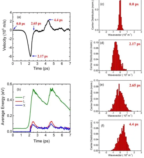
Fig.5.8: (a) Calculated carrier average velocity driven by the quasi-single-cycle pulses with a peak field of 160 kV/cm. (b) average carrier energy at three valleys. The carrier momentum distribution at (a) 0.0 ps. (b) 2.17 ps. (d) 2.65 ps and (d) 4.4 ps. ... 61
Fig.5.9: HHG from single-cycle and multi-cycle THz pulses centered at 0.2 THz (Simulation). (a) nonlinear current density driven by single-cycle THz pules centered at 0.2 THz. The applied peak field is 180 kV/cm. trelax corresponds to the carrier relaxation time and tETHz represents the acceleration time to scatter the carriers to side valleys. (b) the intensity spectra of the Ein and Etrans. The intensity is normalized to the peak intensity of Ein. (c) nonlinear current density driven by multi-cycle THz pules centered at 0.2 THz. The peak incident field used here is 350 kV/cm. (d) the normalized intensity spectra of the Ein and Etrans. ... 64
Fig.6.1: (a) Experimental-setup. The THz pulse energy is measured using a calibrated Golay Cell. (b) THz Michelson interferometer is used to retrieve the THz spectra. (c) THz intensity spectra.
Fig.6.2: Z-scan normalized transmission (enhancement ratio) of various THz pulse energies measured by the Golay cell. All the transmitted THz energies are normalized to the transmitted THz energy at Z = -15.3 mm. ... 70
Fig.6.3: (a) Transmitted energy ratio between InGaAs sample and bare InP substrate versus the incident THz pulse energy at different Z-scan positions. (b) Calculated results by the described intraband model, where the time-domain simulations are performed at each 50 μm. ... 71
Fig.6.4: Incident and calculated transmitted THz waveforms (a), (c), (e) as well as the corresponding average carrier energy (b), (d), (f) at 0.15, 0.3 and 1 MV/cm, respectively. ... 74
Fig.7.1: (a) A photo of the ZnSe based iLAPCA with crossed electrodes. (b) a combination of shadow and binary phase mask is used here to generate THz pulses with tunable ellipticity. Three phase plates can be placed before the vertically or horizontally oriented electrodes. ... 78
Fig.7.2: Transmitted THz waveforms through the bare InP substrate Eref as well as the InGaAs sample Etrans with different thickness of phase masks of (a) 1, (b) 0.2 and (c) 0.12 mm... 79
Fig.7.3: Experimental set-up. We use a polarization state analyzer that is composed of two liquid crystal variable retarders and a Wollaston prism. ... 81
Fig.7.4: Schematic diagram of the detection system with a polarization state analyzer (PSA), which is composed of two liquid crystal variable retarders (LCVR) and one Wollaston prism. . 83
Fig.7.5: Temporal Stokes parameters of the probe beam (a) S0, (b) S1, (c) S2, and (d) S3. (e) The extracted THz signals by using the system with a PSA and by using the conventional EO sampling technique. ... 86
Fig.7.6: Temporal Stokes parameters of the probe beam (a) S1, and (b) S3. (c) Measured THz signals by using the system with a PSA and by using the conventional EO sampling technique. 87
Fig.7.7: Temporal Stokes parameters of the probe beam (a) S1, (b) S2, and (c) S3. (d) Measured 3D THz waveform. ... 89
Publications during the PhD
[1]. X. Chai, X. Ropagnol, L. Sanchez Mora, S. Mohsen Raeis-Zadeh, S. Safavi-Naeini, F. Blanchard and T. Ozaki, “Stokes-Mueller method for full characterization of coherent terahertz waves with ultrahigh dynamic range.” (to be submitted).
[2]. X. Chai, X. Ropagnol, S. Mohsen Raeis-Zadeh, M. Reid, S. Safavi-Naeini, and T. Ozaki. “Subcycle nonlinear terahertz optics with elliptically polarization”, (to be submitted).
[3] X. Chai, X. Ropagnol, A. Ovchinnikov, O. Chefonov, A. Ushakov, C. M. Garcia-Rosas, E. Isgandarov, M. Agranat, T. Ozaki, and A. Savel’ev. “Observation of crossover from intraband to interband nonlinear terahertz optics.” Optics Letters 43, no. 21: 5463, (2018).
[4]. F. Blanchard, X. Chai, X., T. Tanaka, T. Arikawa, T. Ozaki, R. Morandotti, and K. Tanaka, “Terahertz microscopy assisted by semiconductor nonlinearities.” Optics Letters, 43(20), 4997, (2018).
[5]. X. Chai, X. Ropagnol, S. Mohsen Raeis-Zadeh, M. Reid, S. Safavi-Naeini, and T. Ozaki. “Subcycle Terahertz Nonlinear Optics.” Physical Review Letters 121, no. 14: 143901, (2018).
[6]. O. V. Chefonov, A. V. Ovchinnikov, S. A. Romashevskiy, X. Chai, T. Ozaki, A. B. Savel’ev, M. B. Agranat, and V. E. Fortov. “Giant self-induced transparency of intense few-cycle terahertz pulses in n-doped silicon.” Optics Letters 42, no. 23: 4889, (2017).
[7]. X. Ropagnol, X. Chai, S. M. Raeis-Zadeh, S. Safavi-Naeini, M. Kirouac-Turmel, M. Bouvier, C. Côté, M. Reid, M. A. Gauthier, and T. Ozaki. “Influence of Gap Size on Intense THz Generation From ZnSe Interdigitated Large Aperture Photoconductive Antennas.” IEEE Journal of Selected Topics in Quantum Electronics 23, no. 4: 1, (2017).
[8]. H. A. Hafez, X. Chai, Y. Sekine, M. Takamura, K. Oguri, I. Al-Naib, M. M. Dignam, H. Hibino, and T. Ozaki. “Effects of environmental conditions on the ultrafast carrier dynamics in graphene revealed by terahertz spectroscopy.” Physical Review B 95, no. 16: 165428, (2017).
[9]. H. A. Hafez, X. Chai, A. Ibrahim, S. Mondal, D. Férachou, X. Ropagnol, and T. Ozaki. “Intense terahertz radiation and their applications.” Journal of Optics 18, no. 9: 093004, (2016).
[10]. H. A. Hafez, P. L. Lévesque, I. Al-Naib, M. M. Dignam, X. Chai, S. Choubak, P. Desjardins, R. Martel, and T. Ozaki. “Intense terahertz field effects on photoexcited carrier dynamics in gated graphene.” Applied Physics Letters 107, no. 25: 251903(2015).
Patent
[1]. X. Chai and T. Ozaki, “Method and system for terahertz radiation detection and characterization”, US deposition reference: 14448. 168.
Contributions to international conferences during the PhD
[1]. X. Ropagnol, X. Chai, M. Raeiszadeh, S. Safavi-Naeini, M. Reid, and T. Ozaki. “Intense THz Source of Sub-Cycle Pulses with Tunable Elliptical Polarization.” In 2018 43rd International Conference on Infrared, Millimeter, and Terahertz Waves (IRMMW-THz), IEEE, 2018.
[2]. X. Chai, X. Ropagnol, M. Raeiszadeh, S. Safavi-Nacini, M. Reid, and T. Ozaki. “Subcycle Nonlinear Terahertz Optics in Doped Semiconductor Thin Film.” 43rd International Conference on Infrared, Millimeter, and Terahertz Waves (IRMMW-THz), IEEE, 2018.
[3]. X. Chai, X. Ropagnol, M. Raeiszadeh, S. Safavi-Naeini, M. Reid, M. A. Gauthier, and T. Ozaki. “Extreme nonlinear carrier dynamics induced by intense quasi-half-cycle THz pulses in n-doped InGaAs thin film.” In CLEO: QELS_Fundamental Science. Optical Society of America, 2017.
[4]. H. A. Hafez, P. L. Lévesque, I. Al-Naib, M. M. Dignam, X. Chai, S. Choubak, P. Desjardins, R. Martel, and T. Ozaki. “Optical-pump/intense-THz-probe spectroscopy of gated graphene.” In Infrared, Millimeter, and Terahertz waves (IRMMW-THz), 2016.
[5]. X. Chai, H. A. Hafez, I. Al-Naib, Y. Sekine, M. Takamura, K. Oguri, M. M. Dignam, H. Hibino, and T. Ozaki. “Effects of environmental changes on the carrier dynamics in graphene revealed by terahertz spectroscopy.” In Infrared, Millimeter, and Terahertz waves (IRMMW-THz), 2016.
[6]. X. Chai, X. Ropagnol, M. Raeiszadeh, S. Safavi-Naeini, M. Reid, M. A. Gauthier, and T. Ozaki. “Nonlinear ultrafast terahertz waveform modulation in highly n-doped In0.53Ga0.47As thin film.” In Infrared, Millimeter, and Terahertz waves (IRMMW-THz), 2016.
[7]. H. A. Hafez, X. Chai, P. Lévesque, I. Al-Naib, M. Dignam, P. Lassonde, N. Thiré, F. Légaré, R. Martel, and T. Ozaki. “Carrier dynamics in gated graphene revealed by tunable-infrared-pump/terahertz-probe spectroscopy.” In CLEO: Science and Innovations. Optical Society of America, 2016.
[8]. H. H. Eid, P. Lévesque, I. Al-Naib, M. M. Dignam, X. Chai, D. Ferachou, R. Martel, and Ozaki, T. Ozaki. “Intense terahertz field-induced carrier dynamics in gated monolayer graphene.” In CLEO: Science and Innovations. Optical Society of America, 2015.
Chapter 1
Introduction
Terahertz (THz) radiation represents the electromagnetic spectrum that lies between the microwave and the far-infrared [1-3]. The typical THz window corresponds to the frequency range between 0.1 and 10 THz. In particular, this frequency range was called the “THz gap” due to the lack of efficient and compact table-top THz sources and detectors. During the last two decades, with the rapid development of THz sources and detection techniques, this commonly known “THz gap” has now become obsolete [3,4]. Efficient table-top THz sources, detectors and their applications have been facilitated by the advancement of the mode-locked femtosecond laser systems, which led to a fast progress in the applications of various fields, such as condensed matter physics, ultrafast photonics, biomedicine and communications [1,2].
One of the most interesting properties of this specific frequency range is its relatively low photon energy. For example, a 1 THz photon possess a photon energy of 4 meV, which is much smaller than the energy gap of common semiconductor materials. As a result, one can use THz spectroscopy to perform a straightforward contact-free and non-invasive detection of the ultrafast intraband carrier transport in doped semiconductor materials, or to monitor the relaxation of photoexcited carriers in semiconductors [4-6]. Hence, THz spectroscopy becomes a very convenient tool for the investigation of ultrafast carrier dynamics, which is essential for the applications of high-speed electronics and optoelectronics.
During the last decade, various THz sources and detection techniques have been developed using the laser facilities of the Advanced Laser Light Source (ALLS) at the INRS-EMT. The generated THz pulse energies have increased from a few nJ up to several μJ [7-14]. Different techniques have been used, such as photoconductive generation, optical rectification as well as the relativistic plasma THz source. These THz sources possess different characteristics and can be used in different applications. In this study, we focus on THz generation from the nonlinear crystal LiNbO3 via optical rectification and the THz waves generated by a large-aperture photoconductive antenna.
In Chapter 2, we will discuss in detail these two THz generation techniques and the electro-optic sampling technique for coherent THz detection. Then, we will describe THz time-domain spectroscopy as well as optical-pump THz-probe spectroscopy. In Chapter 3, we will present the results of nonlinear THz spectroscopy of graphene and discuss the THz nonlinearities induced by scattering effects. In Chapter 4, we will discuss the limitation of the conventional Drude model and the importance of taking into account the time-scale of the nonlinearities. Then in Chapter 5, we will present the central content of this thesis --- subcycle nonlinear THz optics. We will present results of experiments on nonlinear spectroscopy of a doped semiconductor thin film along with detailed analysis and discussions, supported by ensemble Monte-Carlo simulation. In Chapters 6 and 7, we will discuss the role of interband carrier dynamics on the nonlinear THz responses and the initial experimental results using an elliptically polarized THz pulses, which also include a new detection method for such experiments.
Chapter 2
Nonlinear time-resolved terahertz spectroscopy
A great advantage of THz spectroscopy is that it allows a time-resolved electric field measurement, which is due to its pump-probe configuration nature. This is achieved by a fully coherent generation and detection configuration used in the THz spectroscopy system. In this section, we will start by discussing the THz generation and detection techniques with femtosecond laser systems, then introduce the technique of THz time-domain spectroscopy (THz-TDS) and optical-pump THz-probe (OPTP) spectroscopy.
In the presence of a medium, the generation of electromagnetic radiation can be described by the wave equation:
∇2𝐸 − 𝜀𝜇𝜕2𝐸 𝜕𝑡2 = 𝜇
𝜕𝐽
𝜕𝑡 (2.1) Here, 𝜇 is the permeability, 𝜀 is the permittivity of the medium and is 𝐸 the electric field. 𝐽 can be induced by acceleration of free charge carriers or by oscillating bound electrons. A 𝐽(𝑡) that evolves on the time scale of a few hundred femtoseconds to a few picoseconds will lead to the generation of electromagnetic waves in the THz frequency range. In this study, two THz sources are used, which are the photoconductive antenna (PCA) THz source and the THz source based on optical rectification (OR) in a nonlinear crystal. The PCA source is based on the acceleration of photoexcited carriers 𝐽(𝑡) and on the other hand, OR is due to the anharmonically oscillating bound electrons (or polarization) in a noncentrosymmetric crystals.
2.1 Photoconductive antenna terahertz source
Fig.2.1: Schematic diagram of the THz generation from a photoconductive antenna. A bias voltage
𝐕𝐛 is applied on the semiconductor substrate to drive the photoexcitation carriers.
The principal mechanism of THz generation from PCA is the surge current of photoexcited carriers accelerated by a bias field. For intense THz generation, large-aperture PCA (LAPCA) are normally used to increase the photoexcited area. Fig. 2.1 gives a schematic diagram of a LAPCA THz source with two electrodes deposited on a high-resistivity semiconductor substrate. Here, the femtosecond laser pulse, with a photon energy that is slightly higher than the bandgap of the semiconductor crystal, serves as a transient switch to generate free carriers in the substrate. Conversely to other THz source, the energy of the THz pulse is principally extracted from the DC field applied to the substrate rather than the optical energy.
surface current in the substrate, the relation between the generated THz field in the far field and the applied DC field can be expressed as [1,2,4,6]:
𝐸𝑇𝐻𝑧(𝑡) ∝ 𝜕𝐽𝜕𝑡 ∝ 𝐸𝑏𝜕𝜎(𝑡)𝜕𝑡 (2.2) Here, 𝐸𝑇𝐻𝑧(𝑡) is the generated THz field in the far field, 𝐸𝑏 is the bias electric field and 𝜎(𝑡) is the photoconductivity. The detailed derivation can be found in [1,15]. As can be seen from the relationship between the THz field 𝐸𝑇𝐻𝑧(𝑡) and the applied bias field, the generated THz peak field scales linearly with the bias field. In practice, this feature serves as the central guideline for the choice of the substrate material as well as the design of the antenna structure. For example, due to its relatively low breakdown field (≈ 10 𝑘𝑉/𝑐𝑚), semiconductor GaAs can only be used for conventional low-energy THz sources. Other wide bandgap materials such as ZnO and GaN have been demonstrated as better candidates for high-power LAPCA THz sources [16,17]. Since the laser wavelength we use at ALLS is at 800 nm, the semiconductor ZnSe was chosen as the substrate material for LAPCA [11]. It possesses a bandgap of 2.7 eV and therefore free carriers can be photoexcited by the second harmonic (400 nm) of a Ti:Sapphire laser system. With regard to the antenna structure, interdigitated LAPCA (iLAPCA) structure is currently the most widely used design for high-power THz source [4,15]. Ropagnol et al. [11,13] has developed a ZnSe based iLAPCA THz source at ALLS since 2013, and in 2016, with a surface area of 12.2 𝑐𝑚2, a quasi-half-cycle THz pulse with an energy of 8.3 ± 0.3 𝜇𝐽 was generated. As shown in Fig. 2.2, iLAPCA possesses a large photoexcitation surface area and furthermore, due to the reduced distance between different pairs of electrodes, relatively high-voltage source is not required in the experiment.
Fig.2.2: A photo of the iLAPCA source (without binary mask) developed at ALLS.
A second approach to increase the output THz power is by increasing the number of the generated free carriers with high pumping fluence. However, a saturation of THz emission from LAPCA will take place at high pump fluences due to the screening of the bias field by the emitted THz field [4,15]. As a result, when the LAPCA is operating in a saturation regime, the energy of the generated THz pulses become insensitive to the fluctuation of the pumping optical beam fluence. This saturation effect can then make iLAPCA a suitable THz source to operate at a low repetition rate laser system. As long as the iLAPCA is working under saturation regime, a good shot-to-shot stability can be easily achieved, which is essential for spectroscopic measurements if laser systems with low repetition rate are used. For example, the ZnSe iLAPCA source developed
enough laser energy for the generation of pump pulse (approximately 15 mJ) at 400 nm to photoexcite the relatively large ZnSe substrate.
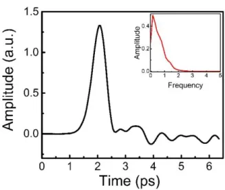
Fig.2.3: THz pulses generated from a ZnSe based iLAPCA THz source. The inset shows the corresponding spectrum. Here, the long negative half-cycle is cut at 6.4 ps due to the overlap with the back reflected pulses from the detection crystal, substrate of the studied sample and the antenna substrate.
Fig. 2.3 shows a typical THz pulse generated from our iLAPCA THz source. One unique property of the THz pulses generated from this iLAPCA is the strong asymmetry in the magnitude of the positive and negative components of the THz profile. This is caused by the rapid carrier acceleration followed by a slow reduction of the current density due to the long carrier relaxation from the conduction band to the valence band [15]. Hence, a quasi-half-cycle THz pulse is naturally generated. The second unique property of the generated THz waves is its low frequency, typically in the low THz frequency range between 0.05 and 1 THz. In the time domain, this
corresponds to a very long half-cycle duration with a high ponderomotive energy, which is advantageous for many applications such as free carrier acceleration.
2.2 Optical rectification
Optical rectification (OR) is a second-order nonlinear effect that takes place when the applied optical field is sufficiently strong to induce large electron displacements from equilibrium in a noncentrosymmetric crystal. The radiated THz field is expressed by the following equation [4,9]: 𝐸𝑇𝐻𝑧 ∝ 𝜕𝐽𝑏𝑜𝑢𝑛𝑑⁄𝜕𝑡= 𝜕2𝑃(𝑡) 𝜕𝑡⁄ 2 (2.3) By assuming two frequency components of the driving light field, 𝐸1(𝑡) = cos(𝜔1𝑡) and 𝐸2(𝑡) = cos(𝜔2𝑡), the second-order polarization 𝑃(2)(𝑡) can be described by:
𝑃(𝑡) ∝ 𝜒(2)cos(𝜔1𝑡) cos(𝜔2𝑡) =𝜒2(2)[cos(𝜔1+ 𝜔2)𝑡 + cos(𝜔1− 𝜔2)𝑡] (2.4) Here, 𝐸𝑜𝑝𝑡 is the electric field of the pump beam and 𝜒(2) is the second-order electric susceptibility tensor. The first term in Eq. (2.3) is relevant for higher harmonic generation and the second term, which is the frequency difference, corresponds to the optical rectification. The interaction with intense laser field results in a quasi-DC polarization, leading to difference frequency generations in the THz frequency range. Hence, choosing the nonlinear crystals with high nonlinear coefficient at the optical pump wavelength is important for the improvement of the optical-to-THz conversion efficiency. For example, the most widely used nonlinear crystals at
crucial to build up the energy of the THz pulses. For example, ZnTe or DAST enables a simple collinear experimental configuration at 800 nm. However, the nonlinear coefficient of the ZnTe crystal is relatively low and high energy THz pulses can only be generated by using large aperture ZnTe crystal [7]. On the other hand, although organic crystals such as DAST possess higher conversion efficiency, they normally suffer from lower damage threshold compared with inorganic crystals [4,9]. The inorganic crystal LiNbO3 is currently being used as an intense THz source in many THz laboratories. Due to the large difference in the refractive indices, a noncollinear configuration must be used to achieve proper phase matching conditions. For optical-to-THz conversion, the following two relations need to be fulfilled for conservation of energy and momentum:
∆𝜔 = 𝜔1− 𝜔2 = Ω𝑇𝐻𝑧 (2.5) ∆𝑘 = 𝑘1− 𝑘2 = 𝐾𝑇𝐻𝑧 (2.6) This leads to the phase matching conditions in the infinitesimal limit:
𝑣𝑇𝐻𝑧,𝑝ℎ𝑎𝑠𝑒 = Ω𝑇𝐻𝑧
𝐾𝑇𝐻𝑧 =
𝜕𝜔
𝜕𝑘 = 𝑣𝑜𝑝𝑡,𝑔𝑟 (2.7) The group velocity of the optical pump must be equal to the phase velocity of the THz waves. For stoichiometric LiNbO3, the optical group index 𝑛𝑜𝑝𝑡 is 2.25 for a pump wavelength 𝜆𝑝𝑢𝑚𝑝 of 800 nm, while the THz phase refractive index is 4.96. As a result, phase matching condition can only be fulfilled at an angle of 𝛾 = 63°, which gives:
𝑣𝑇𝐻𝑧,𝑝ℎ𝑎𝑠𝑒 = 𝑣𝑜𝑝𝑡,𝑔𝑟cos 𝛾 (2.8) Experimentally, this can be realized by titling the pulse front using a diffraction grating.
Fig.2.4: Schematic diagram of the THz generation by using titled-pulse-front technique in a LiNbO3
crystal.
As shown in Fig. 2.4, with an incident angle 𝛼, the diffraction angle 𝛽 is defined through the grating equation sin 𝛼 + sin 𝛽 = 𝑚𝑁𝜆 , where 𝑚 is the diffraction order and 𝑁 is the grove-density of the grating. Using a converging-lens with a demagnification factor 𝐹, the relation between 𝛾 and 𝛽 is given as:
tan 𝛾 =𝑛𝑚𝐹𝑁𝜆
𝑜𝑝𝑡cos 𝛽 (2.9)
Here, the LiNbO3 crystal is cut at this angle in order to provide a normal output angle for the generated THz radiation.
Fig.2.5: Quasi-single-cycle THz pulses generated from a LiNbO3 crystal via OR. The inset shows the
corresponding spectrum.
A typical THz pulse generated from the LiNbO3 source is shown in Fig. 2.5. Quasi-single-cycle THz pulses are generated, and the central frequency normally lies around 0.75 THz. It is important to note that this frequency is approximately 5 times higher than that of the central frequency generated by the iLAPCA THz source (inset of Fig. 2.3). As we will discuss in the following chapters, even though they are both table-top THz sources, this difference may lead to very different experimental observations of nonlinear THz optics.
Due to the high conversion efficiency at 800 nm, the LiNbO3 source based THz-TDS system can work with a high repetition rate laser system. The system used in this work was developed on the 2.5 kHz beamline of ALLS, giving rise to a high sensitivity, a better signal-to-noise ratio as well as fast scanning speed. The optical-pump THz-probe experiment was performed on this setup. The peak electric field of this THz source is between 60 and 70 kV/cm and a pair of wire-grid polarizers is used to vary the incident THz electric field on the investigated sample.
2.3 Electro-optic sampling technique
THz detection is the opposite process of generation and it can be realized by using either PCA or electro-optic (EO) sampling technique on a nonlinear crystal. The EO sampling technique utilizes the Pockels effect, which is analogous to THz generation by OR and is very popular due to its simplicity [1,2,18]. Here, a static (THz) electric field induces birefringence in nonlinear crystals such as ZnTe and GaP, and then modulates the polarization state of the transmitted optical beam.
Fig.2.6: (a) Schematic diagram of the THz detection system using EO sampling technique. (b) A femtosecond laser pulse serves as an ultrafast detector to scan the THz waveforms.
A standard EO sampling detection system is shown in Fig. 2.6. A quarter-wave plate and a Wollaston prism are typically used for a balanced detection via two photodetectors. By using an optical delay stage, the femtosecond optical pulse can thus scan the THz temporal profile point by point, which makes THz-TDS extremely powerful because both amplitude and phase are resolved directly.
and comparison to the technique described in Chapter 7.3, where we present an improved EO sampling approach based on the Stokes-Mueller formalism.
The Stokes vector represents the full polarization state of light, and the effect of a particular optical element is described by a 4 × 4 Mueller matrix [19]. A Stokes vector contains four elements 𝑆0, 𝑆1, 𝑆2 and 𝑆3. The first parameter 𝑆0 represents the total light intensity. Then 𝑆1 corresponds to the intensity difference between the horizontal and vertical polarization component. The third element 𝑆2 is the intensity difference between two linear polarization components orientated at ±45° and the last element 𝑆3 represents the intensity difference between right- and left-hand circular polarization. Here, only 𝑆0 is observable in practice. We use a horizontally linearly polarized probe beam for THz detection and its corresponding Stokes vector can be written as: 𝑆𝑖𝑛 = ( 1 1 0 0 ) (2.10)
When the Pockels effect takes place, the detection crystal can be treated as a wave plate with its birefringence controlled by the THz electric field. For a (110) ZnTe or GaP detection crystal, the phase retardation 𝜙 experienced by the probe beam over a thickness of 𝑑𝐸𝑂 is given as [2]: 𝜙 = 𝜔0𝑑𝐸𝑂
2𝑐 𝑛0 3𝑟
41𝐸𝑇𝐻𝑧√1 + 3𝑐𝑜𝑠2𝛼 (2.11) Here, 𝜔0 is the optical frequency of the probe beam, , 𝑐 is the speed of light, 𝑛0 is the refractive index at the optical probe wavelength and 𝑟41 is the nonlinear coefficient of the specific nonlinear crystal. For a typical THz spectroscopy system, the THz polarization orientation 𝛼 is fixed horizontally (0°) and the generated refractive-index axes (𝜃) are along ±45° according to the following equation [20]:
𝑐𝑜𝑠2𝜃 = 𝑠𝑖𝑛𝛼
√1+3𝑐𝑜𝑠2𝛼 (2.12) We use the Mueller matrix of a waveplate (𝑀𝐸𝑂) with its axis oriented at ±45°:
𝑀𝐸𝑂 = ( 1 0 0 𝑐𝑜𝑠𝜙 0 0 0 𝑠𝑖𝑛𝜙 0 0 0 −𝑠𝑖𝑛𝜙 10 𝑐𝑜𝑠𝜙0 ) (2.13)
And the transmitted Stokes vector of the probe beam is then obtained by multiplying 𝑀𝐸𝑂 with 𝑆𝑖𝑛:
𝑆𝑇𝐻𝑧 = ( 1 cos𝜙 0 −sin𝜙 ) = 𝑀𝐸𝑂∗ 𝑆𝑖𝑛 (2.14)
Then after transmitted through a quarter-wave plate (𝑀𝜆/4) with orientation of 45° and a Wollaston prism (vertically 𝑀𝑉𝑃 and horizontally 𝑀𝐻𝑃 linear polarizer), the final differential vector 𝑆𝑑𝑖𝑓𝑓 before for the two photodetectors becomes:
𝑀𝜆/4 = ( 1 0 0 0 0 00 1 0 0 0 −1 1 00 0 ) (2.15) 𝑀𝑉𝑃 = ( 1 −1 −1 1 0 00 0 0 0 0 0 0 00 0 ) ∗ 0.5 (2.16) 𝑀𝐻𝑃 = ( 1 1 1 1 0 00 0 0 0 0 0) ∗ 0.5 (2.17)
𝑆𝑑𝑖𝑓𝑓 = 𝑀𝑉𝑃∗ 𝑀𝜆/4∗ 𝑆𝑇𝐻𝑧− 𝑀𝐻𝑃∗ 𝑀𝜆/4∗ 𝑆𝑇𝐻𝑧 = ( sin𝜙 −1 0 0 ) (2.18)
As can be seen from equation (2.18), the lock-in amplifier measures straightforwardly the differential signal that is proportional to sin𝜙. Since this can be realized with a very simple experimental configuration, EO sampling technique have become the most widely used THz detection method in the THz community.
However, the one-dimensional measurement of sin𝜙 also causes two problems for intense THz detection. Firstly, a small-angle approximation must be used, because the linear relationship no longer preserves when the phase retardation 𝜙 becomes larger. Secondly, when the phase delay is above 𝜋 2⁄ , an over-rotation will take place due to the symmetric nature of the sinusoidal function around 𝜋 2⁄ [21]. These problems are two of the limitations of the EO sampling technique, which affects strongly the detection dynamic range [22]. In Chapter 7.3, we will introduce an improved EO sampling technique that solves this problem naturally, and can also provide additional information on the THz polarization orientation.
2.4 Terahertz time-domain spectroscopy
Fig.2.7: Schematic diagram of a THz-TDS set-up.
Since both amplitude and phase can be resolved directly, THz-TDS is an extremely powerful and convenient technique for investigating the dielectric properties of the material. Fig. 2.7 shows a typical THz-TDS system with a LiNbO3 THz source. All the THz-TDS systems possess a similar configuration, in which the optical laser beam is separated into two parts. One part is used for THz
crystal. To perform nonlinear measurements, one can use a pair of wire-grid polarizers to tune the incident THz intensity, or change the applied bias voltage on an iLAPCA THz source.
Fig.2.8: Normal incidence and transmission of THz electric field through a thin conducting film deposited on a dielectric substrate: (a) substrate - thin film configuration and (b) thin film – substrate configuration, where another Fresnel loss at the substrate-air interface should be taken into account for the measured field by EO sampling.
Two measurements are required for THz-TDS: one reference waveform measured in air 𝐸𝑖𝑛(𝑡) or with a substrate of known dielectric properties 𝐸𝑟𝑒𝑓(𝑡), and a second waveform 𝐸𝑡𝑟𝑎𝑛𝑠(𝑡) measured after transmission through the whole sample. Here, we will focus on a special case, where the sample is composed of one thin conducting film deposited on a semi-insulating substrate. In this thesis, both the n-doped semiconductor In0.53Ga0.47As sample as well as the graphene sample possess such configuration. In the thin-film limit, since the wavelength and skin depth are much larger than the thickness of the conducting film, the driving THz field is assumed to be uniform for all the charge carriers. The thin-film transmission equation in the time domain is given by [23]:
𝐸𝑡𝑟𝑎𝑛𝑠(𝑡) =𝑌 1
0+𝑌𝑆(2𝑌0𝐸𝑖𝑛(𝑡) − 𝐽(𝑡)𝑑) (2.19)
Here, 𝑑 is the thickness of the thin film. 𝑌0 = (377 Ω)−1 is the free-space admittance, 𝐽(𝑡) is the current density, and 𝑌𝑠 = 𝑁𝑌0 is the admittance of the substrate, in which N is the refractive
index of the substrate. All the carriers in the thin film are assumed to experience the same driving field 𝐸𝑡𝑟𝑎𝑛𝑠(𝑡). It is important to note that a Fresnel loss due to the transmission through the substrate-air interface should be taken into account to calculate the transmitted field in the air measured by the detection crystal.
As shown in Fig. 2.8, during the experiment, the sample can be placed in one of two possible configurations, substrate – thin film (Fig.2.8(a)) or thin film – substrate (Fig. 2.8(b)). Here, equation (2.19) corresponds to the experimental configuration of thin film – substrate. In fact, the two systems may lead to very different nonlinear THz transmissions and it is thus important to distinguish them in detail. As discussed in the following, nonlinear transmission could be much stronger for the configuration of substrate – thin film of Fig. 2. 8 (a). In this case, the incident THz field experiences first a Fresnel loss and the amplitude reduces to 2/(𝑁 + 1) of the original field strength. In the thin film transmission equations, the free-space admittance 𝑌0 also needs to be changed to 𝑌𝑠 before 𝐸𝑖𝑛(𝑡). The obtained THz transmission equation then becomes as:
𝐸𝑡𝑟𝑎𝑛𝑠(𝑡) =𝑌 1
0+𝑌𝑆(
4𝑌𝑆
𝑁+1𝐸𝑖𝑛(𝑡) − 𝐽(𝑡)𝑑) (2.20) By comparing the two factors before 𝐸𝑖𝑛(𝑡) between equation (2.20) and equation (2.19), we obtain an increase ratio of 2𝑁 (𝑁 + 1)⁄ . Hence, for any substrate material with a refractive index of 𝑁 > 1, the applied field on the thin conducting layer is higher for the configuration of substrate
– thin film – air. For example, a refractive index of 3 will lead to an enhancement factor of 1.5,
2.5 Optical-pump terahertz-probe spectroscopy
Fig.2.9: (a) Schematic diagram of an optical/IR-pump THz-probe system (b) Differential transmission signal of a photoexcited GaAs substrate.
The THz-TDS system is based on a THz-pump optical-probe configuration, and as a result we can retrieve the THz signal in the time domain using an EO sampling technique. On the other hand, we can also use the THz pulse to serve as a probe signal on the studied sample. For example, one widely used technique is optical-pump THz-probe (OPTP) spectroscopy. Here, a sample is photoexcited optically and then the THz pulse is used to probe the transient changes on the conductivities after photoexcitation. A schematic diagram of the experimental set-up is shown in Fig. 2.9 (a). Compared with the THz-TDS system, an extra delay line is added to tune the time delay between the optical pump and the THz pulse. Another optical chopper is used here on the pump line to obtain the differential signal ∆𝑇 𝑇⁄ , which measures the change in the material 0 property before and after photoexcitation with different time delays. Fig. 2.9 (b) shows the
measured differential signal ∆𝑇 𝑇⁄ of a photoexcited GaAs semiconductor. The optical pump 0 generates free charge carriers within the semiconductor sample and as a result we observe a THz absorption enhancement or transmission reduction with negative ∆𝑇 𝑇⁄ . Due to the huge signal 0 variation before and after photoexcitation, a bare substrate of GaAs or silicon is normally used to find the zero-time position of the OPTP experimental setup.
Chapter 3
Terahertz spectroscopy of graphene
3.1 Terahertz electrodynamics of graphene
Graphene is a monolayer of carbon atoms arranged in a honeycomb lattice [24]. This unique structure led to a gapless, linear band dispersion with charge carriers behaving as massless Dirac fermions [24,25]. Many of graphene’s spectacular transport and optical properties are a direct consequence of this unique band structure. In contrast to usual semiconductor systems with parabolic or non-parabolic dispersion, the absolute value of the electron velocity is a constant (Fermi velocity 𝑣𝐹 = 106 m/s) [24,25]. Assuming an incident monochromatic THz wave:
𝐸𝑇𝐻𝑧(𝑡) = 𝐸𝑇𝐻𝑧cos 𝜔𝑡 (3.1) and neglecting the interband transition, a strongly anharmonic temporal current density will thus be generated:
𝐽(𝑡) ∝ 𝑣𝐹sign[sin 𝜔𝑡] (3.2) Here, the nonlinear effects become important even at small fields and the generated square-wave-like current density will lead to the generation of odd order harmonics [26-28]. This is particularly interesting for applications in the THz frequency domain, because for doped graphene the interband transitions of THz photons are normally Pauli blocked. It has been theoretically predicted that graphene can be used as a natural THz frequency multiplier [26-28]. This was one of the most important motivations to study the nonlinear interaction of graphene with intense THz waves. In reality, on the other hand, due to the single-layer structure, the electronic property of
graphene can be strongly affected by the surrounding medium and various scattering effects [29-33]. The electron mobility of graphene at room temperature is only a few thousands cm2/Vs, with an electron scattering time ranging from 10−14− 10−12 s. As shown in the following discussion, rather than the linear band dispersion, it is the carrier scattering effects that dominate the nonlinear THz responses at high electric fields.
Quantitatively, the electromagnetic responses of graphene can be described in terms of conductivity and separated into interband and intraband absorption. The intraband conductivity describes the intraband charge carrier dynamics and is normally described by a Drude response of a 2D massless Dirac system [34-41]:
𝜎𝑖𝑛𝑡𝑟𝑎(𝜔) = 𝜋(1 𝜏2𝑒⁄2⁄−𝑖𝜔)ℏ2 𝑘𝐵𝑇𝑒ln[2 cosh (𝐸𝐹⁄2𝑘𝐵𝑇𝑒)] = 1 𝜏⁄ 𝐷−𝑖𝜔
(3.1) Here, 𝐸𝐹 is the Fermi-level energy, 𝑇𝑒 is the electron temperature, 𝜏 is the scattering time and 𝐷 is the Drude weight. The interband conductivity, on the other hand, can be expressed by [42-44]:
𝜎𝑖𝑛𝑡𝑒𝑟(𝜔) = 𝑒 2 8ℏ[tanh ( ℏ𝜔+2𝐸𝐹 4𝑘𝐵𝑇𝑒 ) + tanh ( ℏ𝜔−2𝐸𝐹 4𝑘𝐵𝑇𝑒 )] (3.2)
When ℏ𝜔 is higher than 2𝐸𝐹 (without Pauli blocking), a universal absorption of 𝑒2⁄ is obtained 4ℏ at room temperature for visible light. In practice, the graphene samples are normally doped with a certain Fermi energy ranging from approximately 100 meV up to 400 meV [45]. The minimum Fermi energy we have in our gated graphene samples is around 70 meV. As a result, the interband THz absorption is Pauli blocked and the THz conductivity can be fully described by Equation (3.1). The THz conductivity can then be tuned by changing either the Drude weight or the scattering time.
In the following two sections, we will first study the effect of environmental conditions on the carrier dynamics in graphene and then give a brief discussion on the nonlinear THz responses of gated monolayer graphene.
3.2 Ambient temperature effects on the carrier dynamics in graphene
Our group has been studying the interaction of THz radiation with graphene since 2010. By performing nonlinear THz-TDS and optical-pump intense-THz-probe spectroscopy on highly doped epitaxial graphene with a fixed Femi energy, Hafez et al. [39,46] have demonstrated that the combined effect of the optical pump and the THz electric field on the scattering times plays the largest role in defining the induced nonlinear carrier dynamics in monolayer graphene. Using gated graphene, Razavipour et al. [40] have demonstrated that the high-field THz responses of graphene are strongly Fermi energy dependent as well. The nonlinear THz response of graphene is found to be mainly dependent on the presence of free carriers and dominated by the increase in the scattering rate with increasing THz fields. Furthermore, at low Fermi energies, the differential THz transmission after target can be switched between positive and negative by changing the applied THz field strength, which pave the way to the development of optical switching applications [47].
For future technological applications, a thorough understanding of the stability of graphene under ambient environmental conditions is needed and crucial [41]. We then extended our investigations by employing THz-TDS as well as OPTP spectroscopy to study the effects of the ambient temperature on the optoelectronic properties of graphene. This work is in collaborations with Prof. Hiroki Hibino’s group from NTT, Japan and Prof. Dignam’s group from Queen’s University (Kingston, Ontario).
In this experiment, we tested two types of large-scale monolayer graphene samples on the same 4H-SiC substrate, prepared by epitaxial growth methods from 4H-SiC and by transferring the chemical vapor deposited (CVD) graphene to a 4H-SiC substrate. The graphene samples are fabricated and characterized by the NTT group. The CVD graphene samples have shown high (~1012− 1013cm−2) hole doping concentrations, while the epitaxial graphene samples have shown relatively low ( ~1011− 1012cm−2) electron doping. We performed linear THz spectroscopy on the graphene samples in air at various temperatures ranging from room temperature up to 300°C. The sample under test is sandwiched in a specially designed sample holder with two aluminum plates with holes at the center and connected to a coil heater. The THz pulse is generated by optical rectification of 800 nm, 40 fs, Ti:Sapphire laser pulses in a LiNbO3 crystal using the pulse-front tilting technique [4]. In this study, the electric field is kept at minimum of approximately 1.5 kV/cm to avoid any nonlinear effects induced by intense THz electric field.
Fig.3.1: THz-TDS measurements by changing the ambient temperature: the transmitted THz pulses (a) and (c) and the normalized peak field (b) and (d) for p-doped CVD graphene and n-doped epitaxial graphene. Adapted from [43].
Fig. 3.1 (a) and (c) show the THz-TDS measurements by varying the ambient temperatures for CVD and epitaxial graphene. Fig.3.1. (b) and (d) show the corresponding THz peak transmission normalized to THz transmission of the sample at room temperature as a function of the sample temperature. Interestingly, the two graphene samples exhibit almost opposite behaviors as the temperature is increased. The THz transmission of the p-doped CVD graphene generally increases with increasing temperature, while the THz transmission of n-doped epitaxial graphene initially increases slightly but the general trend is a decrease in the transmission as the temperature increases.
Fig.3.2: Ambient temperature effects on the THz photoconductivity of graphene after
photoexcitation: 𝚫𝐓/𝐓𝟎 as a function of the delay time between the optical pump and the THz
probe beams for (a) n-doped epitaxial graphene, (c) p-doped CVD graphene, the black and red arrow indicate the reduction and enhancement of differential transmission by increasing the sample temperature; (b) and (d) are the corresponding peak of 𝚫𝐓/𝐓𝟎 as a function of the temperature for CVD graphene and epitaxial graphene. Adapted from [43].
We then performed OPTP measurements to measure the temperature effects on the differential signals after photoexcitation by an 800 nm optical pump. Fig. 3.2 shows the OPTP response of the graphene samples defined by the THz differential transmission ΔT/T0 after photoexcitation. For the highly p-doped CVD graphene sample, we observe a positive ΔT/T0 at room temperature that decreases monotonically with increasing temperature (as represented by the black arrow), as
On the other hand, the lightly n-doped epitaxial graphene shows a negative ΔT/T0 at room temperature, which interestingly turns positive with increasing temperature, as shown in Fig. 3.2 (c) and 3.2 (d). These observations are analogous to those reported with gated graphene, in which the Fermi energy is changed by electrical gating [37,47,48]. Compared with non-doped semiconductor such as GaAs (Fig.2.9 (b)), graphene is a semi-metal and conductive at room temperature. When the Fermi energies are close to the charge neutral point, the additional carriers provided by the optical pump lead to a negative differential transmission signal, similar to normal semiconductors after photoexcitation. On the other hand, if the initial Fermi energy is already high, increased electron temperature due to photoexcitation may lead to a significant increase of scattering rate and in turn giving rise to a positive differential transmission after photoexcitation as shown here. This can be explained by the change of intraband conductivity as described in equation (3.1), in which the relative variations of the Drude weight and the scattering time determine the sign of the differential signal ΔT/T0 after photoexcitation.
Fig.3.3: Heating effect on the Fermi energy in (a) highly p-doped CVD graphene and (b) lightly n-doped epitaxial graphene. Adapted from [43].
It has been reported in earlier studies that the desorption of air and oxygen molecules away from the surface of graphene can result in reduced hole doping (or equivalently increased electron doping) [29]. As a result, by heating, CVD graphene becomes less p-doped, while epitaxial graphene becomes more n-doped. We have confirmed this hypothesis by performing van der Pauw and Hall-effect measurements at temperatures comparable to those reported here, which have shown a dominant change of carrier density compared with the mobility change [41]. The highly
p-doped CVD graphene with highly Fermi energy in the valence band exemplifying metal-like
properties experienced an increase in the Fermi energy towards the charge neural point without switching to the semiconductor-like regime, resulting only in a reduction in the positive ΔT/T0. In contrast to this, the crossover in the OPTP response of epitaxial graphene from a negative ΔT/T0 to a positive ΔT/T0 can be attributed to temperature-induced increase from a low Fermi energy in the conduction band exemplifying semiconductor-like properties, to higher Fermi energies exemplifying metal-like properties [37,41,47,48]. The Fermi energy thus exceeded a certain value that separates the two regimes when the sample is heated.
In summary, we have demonstrated that the linear THz responses are determined by the number of free charge carriers or the Fermi energy of graphene. The electronic properties of graphene are extremely sensitive to the sample temperature, which can tune the Fermi energy of graphene through desorption of water and oxygen molecules. This paves the way for using graphene in thermal switching and environmental sensing applications. However, this extreme sensitivity can also pose a great challenge in using graphene in many optoelectronic applications that require
3.3 Nonlinear terahertz time-domain spectroscopy of gated graphene
In 2013, in collaboration with Prof. Richard Martel’s group at the University of Montreal, Hafez
et.al. [40,47] designed a graphene device in the form of a field-effect-transistor, in which the
carrier density can be controlled by electrochemical doping with a layer of ionic gel that is transparent in the THz frequency range. By controlling the Fermi-level energy, we can then study both the electric field and carrier density dependency of the nonlinear THz responses of graphene. For this sample, the minimum Fermi energy is 70 meV away from the CNP. Since the ionic gel is not homogenously distributed on the graphene sample, the Fermi energy of graphene for the THz detection region is an average of the detection beam size.
Fig.3.4: Nonlinear THz-TDS of gated graphene: (a) THz peak transmission as a function of the Fermi energy for various THz field strengths. The arrow indicates the transmission enhancement with THz electric field for a certain Fermi energy. (b) Field-dependence of THz peak transmission at different Fermi energies.
We measured the transmitted THz pulses through graphene and the graphene-free part of the sample and plotted the peak transmission as a function of the graphene Fermi energy at various field strengths. As can be seen from Fig. 3.4 (a), the peak transmission reaches the maximum value when the Fermi energy is close to the charge neutral point (CNP). Here, the carrier density is at its minimum and the maximum transmission is a result of the lowest THz conductivity due to the reduced Drude weight. On the other hand, as indicated by the arrow in Fig. 3.4. (a), increasing the THz field results in an increase in the THz transmission, which is more pronounced for graphene with higher doping. When the doping concentration is decreased, the relative increase in transmission with increasing THz field is less pronounced, indicating less nonlinear THz field effects. These observations emphasize that the nonlinear response of the graphene sample is mainly dependent on the presence of free carriers and can be explained by increased scattering when the THz field is increased.
To model the observed nonlinear effects, we account for intraband absorption using Equation (3.1) and take into account neutral (𝜏𝑠𝑟) and charged impurity scattering (𝜏𝐶𝑜𝑢𝑙) as well as optical phonon scattering (𝜏𝑜𝑝) [39,40,46,47]. Two potential types of optical phonons can contribute to scattering: optical phonons in the graphene itself and polar surface phonons in the substrate. Due to the weak coupling strength, the scattering rate contribution from the surface phonons in the substrate materials is much smaller than those due to the graphene optical phonons [40]. As a results, here we only take into account the contributions from the optical phonons in graphene. The scattering time 𝜏 is expressed as:
1 𝜏 = 1 𝜏𝐶𝑜𝑢𝑙+ 1 𝜏𝑠𝑟 + 1 𝜏𝑜𝑝 = 𝐶1 𝐸𝑒𝑓𝑓+ 𝐶2𝜀𝑘+ 𝐷02 2ℏ2𝜐 𝐹 2𝜎 𝑚𝜔0 𝜀𝑘+ℏ𝜔0 𝑒ℏ𝜔0 𝑘𝐵𝑇⁄ −1 (3.3)
where 𝐶1 (3.63 ps−1eV)and 𝐶2 (30 ps−1eV) are constants that depend on the density of the charged and neutral impurities, respectively. 𝐸𝑒𝑓𝑓 is the effective Fermi energy for a given electron temperature, 𝜀𝑘 is the average carrier kinetic energy driven by the THz field, ℏ𝜔0 = 147 meV is the optical phonon energy, 𝐷0 = 5 × 10⁹ eV/cm is the deformation potential for the zone-edge optical phonons, 𝜎𝑚 = 7.6 × 10⁻⁸ g cm⁄ 2 is the 2D mass density of graphene, 𝑘𝐵is the Boltzmann constant and T is the phonon temperature that serves as a fitting parameter for the calculation of the scattering time as shown in Fig. 3.5 (a). High-field THz pulses lead to strong carrier heating and in turn reduce the total scattering time as well as the THz absorption.
In conclusion, we observed a strong increase in the THz transmission with increasing field. This transmission enhancement appears to result from a decrease in the carrier scattering time with increasing electric field. Higher field-induced THz transmission modulation range was observed for graphene with a high Fermi energy. As demonstrated by the ambient temperature effect as well
as the gating effect, the number of carriers that interact with the THz pulses are important for both low- and high-field responses. In addition, by performing OPTP measurements, we have observed a crossover from semiconductor-like to metal-like behavior by increasing the Fermi energy of graphene. The change of the Fermi energy can be realized by changing the ambient temperature of graphene or by control the gate-voltage of the gated graphene. The nonlinear THz responses are similar for both CVD and epitaxial graphene, in which the Fermi energy as well as the scattering rate determines the corresponding nonlinear THz conductivity.
It is worth mentioning that due to the strong carrier scattering effect, we did not observe any signature of THz coherent harmonic generation due to the linear band dispersion. However, another question is also raised here because we didn’t actually lose the nonlinearity. The scattering effect itself takes place during each half-cycle acceleration, resulting in a nonlinear variation of the THz conductivity. In the following sections, we will discuss nonlinear terahertz optics induced by intraband carrier dynamics as well as the importance to take into account the temporal variation of the THz conductivity.
Chapter 4
Nonlinear terahertz optics induced by intraband carrier dynamics
Nonlinear optics refers to the nonlinear behavior of light in a medium, in which the dielectric polarization responds nonlinearly to the electric field of the incident light [49]. For THz-driven free charge carrier dynamics in graphene or in common doped semiconductors [39,40,46,50-53], we use the THz conductivity of the material to describe the corresponding response to the THz electric field. Analogously, for a centrosymmetric system, the nonlinear variation of THz conductivity should have led to the generation of odd-order harmonics. On the other hand, even-order harmonics could be observed in a noncentrosymmetric system. In the following, we will discuss three possible intraband approaches that can be used for nonlinear THz optics.
4.1 Nonlinear THz intraband conductivity
4.1.1 Nonparabolic band dispersion
As discussed in Chapter 3.1, the initial motivation to perform nonlinear THz spectroscopy on graphene was due to its unique linear band dispersion, which should have led to the generation of harmonics even at relatively low fields. In fact, similar effects exist for common semiconductors as well. When an electron occupies higher energy levels in the conduction band, the energy-momentum dispersion deviates from a parabolic dispersion [54]. As a result, the carrier will no