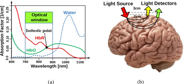
On-Chip Integrated Functional Near Infra-Red Spectroscopy (fNIRS) Photoreceiver for Portable Brain Imaging
192
0
0
Texte intégral
Figure

+7

Documents relatifs