M A UNIVERSITE DE
l a SHERBROOKE
Faculte de genie
Departement de genie electrique et genie informatique
DEPOT EN PHASE VAPEUR ET CARACTERISATION DES COUCHES MINCES A BASE DE POLYMERES DE POLYSILANE ET LEURS APPLICATIONS DANS LES
DISPOSITIFS SEMICONDUCTEURS COMPOSES ET EN SILICIUM
CHEMICAL VAPOR DEPOSITION AND CHARACTERIZATION OF
POLYSILANES POLYMER BASED THIN FILMS AND THEIR APPLICATIONS IN COMPOUND SEMICONDUCTORS AND SILICON DEVICES
These de doctorat es sciences appliquees
Speciality: genie electrique
Composition du jury
Cetin Aktik, Universite de Sherbrooke Mihai Scarlete, Bishop's University
Rejean Fontaine, Universite de Sherbrooke Dominique Drouin, Universite de Sherbrooke Stephane Blain, Dalsa Semiconductor Corporation
El Hassane OULACHGAR
Sherbrooke (Quebec) Canada December 2008
1*1
Library and Archives Canada Published Heritage Branch 395 Wellington Street OttawaONK1A0N4 Canada Bibliotheque et Archives Canada Direction du Patrimoine de I'edition 395, rue Wellington OttawaONK1A0N4 CanadaYour file Votre reference ISBN: 978-0-494-52851-8 Our file Notre reference ISBN: 978-0-494-52851-8
NOTICE: AVIS:
The author has granted a
non-exclusive license allowing Library and Archives Canada to reproduce,
publish, archive, preserve, conserve, communicate to the public by
telecommunication or on the Internet, loan, distribute and sell theses worldwide, for commercial or non-commercial purposes, in microform, paper, electronic and/or any other formats.
L'auteur a accorde une licence non exclusive permettant a la Bibliotheque et Archives Canada de reproduire, publier, archiver, sauvegarder, conserver, transmettre au public par telecommunication ou par I'lnternet, preter, distribuer et vendre des theses partout dans le monde, a des fins commerciales ou autres, sur support microforme, papier, electronique et/ou autres formats.
The author retains copyright ownership and moral rights in this thesis. Neither the thesis nor substantial extracts from it may be printed or otherwise reproduced without the author's permission.
L'auteur conserve la propriete du droit d'auteur et des droits moraux qui protege cette these. Ni la these ni des extraits substantiels de celle-ci ne doivent etre imprimes ou autrement
reproduits sans son autorisation.
In compliance with the Canadian Privacy Act some supporting forms may have been removed from this thesis.
Conformement a la loi canadienne sur la protection de la vie privee, quelques
formulaires secondaires ont ete enleves de cette these.
While these forms may be included in the document page count, their removal does not represent any loss of content from the thesis.
Bien que ces formulaires aient inclus dans la pagination, il n'y aura aucun contenu manquant.
This thesis is dedicated to my sons Haron and Adam and to the memory of my father
ABSTRACT
As the semiconductors industry is moving toward nanodevices, there is growing need to develop new materials and thin films deposition processes which could enable strict control of the atomic composition and structure of thin film materials in order to achieve precise control on their electrical and optical properties. The accurate control of thin film characteristics will become increasingly important as the miniaturization of semiconductor devices continue. There is no doubt that chemical synthesis of new materials and their self assembly will play a major role in the design and fabrication of next generation semiconductor devices.
The objective of this work is to investigate the chemical vapor deposition (CVD) process of thin film using a polymeric precursor as a source material. This process offers many advantages including low deposition cost, hazard free working environment, and most importantly the ability to customize the polymer source material through polymer synthesis and polymer functionalization. The combination between polymer synthesis and CVD process will enable the design of new generation of complex thin film materials with a wide range of improved chemical, mechanical, electrical and optical properties which cannot be easily achieved through conventional CVD processes based on gases and small molecule precursors.
In this thesis we mainly focused on polysilanes polymers and more specifically poly(dimethylsilanes). The interest in these polymers is motivated by their distinctive electronic and photonic properties which are attributed to the derealization of the a-electron along the Si-Si backbone chain. These characteristics make polysilane polymers very promising in a broad range of applications as a dielectric, a semiconductor and a conductor. The polymer-based CVD process could be eventually extended to other polymer source materials such as polygermanes, as well as and a variety of other inorganic and hybrid organic-inorganic polymers.
This work has demonstrated that a polysilane polymeric source can be used to deposit a wide range of thin film materials exhibiting similar properties with conventional ceramic materials such as silicon carbide (SiC), silicon oxynitride (SiON), silicon oxycarbide (SiOC)
silicon dioxde (SiC>2) and silicon nitride (SiaN,*). The strict control of the deposition process allows precise control of the electrical, optical and chemical properties of polymer-based thin films within a broad range. This work has also demonstrated for the first time that poly(dimethylsilmaes) polymers deposited by CVD can be used to effectively passivate both silicon and gallium arsenide MOS devices. This finding makes polymer-based thin films obtained by CVD very promising for the development of high-K dielectric materials for next generation high-mobility CMOS technology.
Keywords: Thin films, Polymers, Vapor Phase Deposition, CVD, Nanodielectrics, Organosilanes, Polysilanes, GaAs Passivation, MOSFET, Silicon Oxynitride, Integrated Waveguide, Silicon Carbide, Compound Semiconductors.
RESUME
Au fur et a mesure que l'industrie des semiconducteurs s'oriente vers les nanodispositifs, il y a un besoin croissant de developper de nouveaux materiaux et procedes de depot de couches minces qui pourraient permettre un controle strict de la composition et de la structure atomique des materiaux, ceci dans le but de realiser un controle precis sur leurs proprietes electriques et optiques. Le controle precis des caracteristiques des couches minces deviendra de plus en plus important avec la miniaturisation des dispositifs semiconducteurs. II n'y a aucun doute que la synthese chimique de nouveaux materiaux et leur auto-assemblage joueront un role tres important dans la conception et la fabrication des dispositifs semiconducteurs de la prochaine generation.
L'objectif de ce travail est d'etudier le procede de depot en phase vapeur (CVD) des couches minces en utilisant un precurseur polymerique comme source. Ce procede offre plusieurs avantages, notamment un cout de deposition relativement bas, un environnement de travail sans risque, et tout particulierement la possibility d'adapter le materiau de la source aux besoins a travers la synthese et la fonctionnalisation des polymeres. La combinaison entre la synthese de polymere et le procede de CVD permettra la conception d'une nouvelle generation de materiaux complexes avec un large eventail de proprietes chimiques, mecaniques, electriques et optiques ameliorees qui ne peuvent pas etre facilement obtenues par des procedes CVD conventionnels bases sur des gaz et des precurseurs moleculaires.
Dans cette these nous nous sommes principalement concentres sur des polymeres de polysilanes et plus specifiquement sur les poly(dimethylsilanes). L'interet porte a ces polymeres est motive par leurs proprietes electroniques et photoniques distinctives, qui sont attribuees a la delocalisation des electron-a le long de la chaine du polymere. Ces caracteristiques rendent les polymeres de polysilanes tres attrayants dans un grand nombre d'applications telles que les dielectriques, les semiconducteurs et les conducteurs. Le procede CVD a base de polymeres peut 6tre eventuellement etendu a d'autres materiaux polymeriques tels que des polygermanes, ainsi qu'a une vaste variete de polymeres inorganiques et organique-inorganiques hybrides.
Ce travail a demontre que les polymeres polysilanes peuvent etre utilises comme source pour deposer un large eventail de materiaux en couche mince presentant des proprietes semblables aux materiaux ceramiques conventionnels tels que le carbure de silicium (SiC), l'oxynitrure de silicium (SiON), le dioxde de silicium (SiC>2), l'oxycarbure de silicium (SiOC), et le nitrure de silicium (Si3N4). Le controle strict des parametres de procede de depot permet un controle precis des proprietes electriques, optiques et chimiques des couches minces dans un large intervalle. Ce travail a egalement demontre pour la premiere fois que les polymeres de polysilanes deposes par CVD peuvent etre utilises pour passiver efficacement des dispositifs MOS a base d'arseniure de gallium et de silicium. Ces resultats rendent les couches minces a base des polymeres, obtenues par CVD, tres prometteuses pour le developpement de materiaux dielectriques hauts-K pour la technologie CMOS a haute mobilite de la prochaine generation.
Mots-cles : Couches minces, Polymeres, Depot en Phase Vapeur, CVD, Nanodielectriques, Organosilanes, Polysilanes, GaAs Passivation, MOSFET, Oxynitrure de Silicium, Guide d'Ondes Integres, Carbure de Silicium, Semiconducteurs Composes
ACKNOWLEDGMENTS
The work on this thesis has been an inspiring, often exciting, sometimes challenging, but always interesting experience. This work would be impossible without the support, encouragement, patience and enthusiasm of many devoted people, who had contributed in many ways to the successful completion of this work. It is impossible for me to mention the name of each person here, but I am truly grateful to everyone who supported this work directly or indirectly.
First of all, I would like to express my most sincere gratitude to my supervisor Cetin Aktik for giving me the opportunity to join his multidisciplinary research group. I have truly enjoyed working with him, and I greatly appreciate his guidance, advices and encouragements. I have enormously benefited from his expertise in compounds semiconductor devices fabrication and characterization as well as thin film materials growth. I am very thankful to Prof. Aktik for helping me obtain access to several external laboratories, and also for giving me the chance to participate in several interesting research projects and to attend various international conferences. Besides of being an excellent supervisor, Cetin was as close as a relative and a good friend to me.
I am deeply indebted to my co-supervisor Dr. Mihai Scarlete at Bishop's University for offering me a valuable support and guidance from the start to the end of this work. I truly appreciate the trust he put in me, by giving me unrestricted access to thin films research laboratory and all the facilities available at the department of chemistry at Bishop's university. I am very grateful for the many hours that Dr. Scarlete spent reviewing and perfecting my works. Through him, I have gained extensive knowledge and experience in polymer materials and physical chemistry, which I believe will be very valuable assets in my future carrier as a researcher. I am very fortunate to meet Mihai, and I hope our friendship and collaboration will continue for many years to come.
I would like also to express my gratitude to Dr. Subhash Gujrathi at the Thin Film Physics and Technology Research Center (GCM) at Montreal University, for his kindness and patience and for the long hours he spent analyzing, and discussing the results of ERD analysis and for taking the time to answer many of my questions.
Special thanks go also to Mme Suzie Poulin at the Materials and Surface Analysis Laboratory (LASM) at Ecole Polytechnique in Montreal, and Mme Sonia Blais at the Centre for Characterization of Materials (CCM) at Universite de Sherbrooke for their great support in conducting the XPS analysis and for spending a great deal of time helping me analyze and interpret the XPS results. My thanks go also to Prof. Denis Morris at the Department of Physics at Universite de Sherbrooke for allowing me to use the PL facilities available at his Spectroscopy Laboratory, and for his valuable support and discussions.
Many thanks go to all the technical support team at the Nanofabrication and Nanocharacterization Research Center (CRN2) for their great support. I would like to particularly thank Pierre Langlois, Pierre Lafrance and Guillaume Bertrand, Michael Lacerte and Gabriel Laliberte for answering many of my questions and for greatly facilitating my work in the cleanroom. I would like also to thank David O'Neill at the department of chemistry at Bishop's University for his great support during experiments setup and chemical analyses.
I am very grateful to Professor Rejean Fontaine and Professor Dominique Drouin at Universite de Sherbrooke and Mr. Stephane Blain at Dalsa Semiconductor Corporation for taking the time to review this thesis and for accepting to be part of the committee of the jury. A special appreciation goes equally to all other members of the jury for their precious time and the particular attention they gave to this work.
I would like also to thank my colleagues and friends, Tahereh Fanaei, Abdou Sana, Starr Dostie, Robert Sowerby, Nathalie Camire, Yousef Awad, and Maxime Lessard for sharing their experience, aspiration and dreams. Through the many years we worked together we shared many exciting and sometimes difficult moments in our lives. I truly appreciate the time we all spent together. I sincerely wish them all success, prosperity and happiness in each and every step of their lives.
Finally and most importantly, I would like to express my deepest gratitude to my family for their tenacious love and support throughout my life. This dissertation is merely unfeasible without them. I am particularly indebted to my mother for her care, tireless love
persistent confidence in me, and for helping me keep my life in proper perspective and balance.
TABLE OF CONTENTS
ABSTRACT iii RESUME v ACKNOWLEDGMENTS vii TABLE OF CONTENTS xi LIST OF FIGURES xv LIST OF TABLES xix LIST OF ACRONYMS xxiCHAPTER 1 1 INTRODUCTION , 1
1.1 Semiconductor technology status and trends 1
1.1 Thin film materials technology 1 1.2 The nanotechnology era 2 1.2 Polymer-based thin film materials 3
1.2.1 Brief introduction to polymers 3 1.2.2 Organic polymer thin films 4 1.2.3 Inorganic polymer thin film 5 1.3 Deposition of Polymer-based thin films 6
1.3.1 Liquid phase deposition processes 6 1.3.2 Vapor phase deposition processes 7 1.4 Silicon based polymeric materials 10
1.4.1 Organosilane polymers 10 1.4.2 Polysilane polymers 11 1.5 Preparation of polysilanes polymer-based thin film 11
1.5.1 Synthesis and functionalization of polysilanes 11 1.5.2 Chemical vapor deposition of polysilanes thin films 12 1.6 Polysilanes polymer-based thin films potential applications 13
1.6.1 LOW-K dielectrics materials 13
1.6.2 High-K dielectrics materials 14 xi
1.6.3 MOSFET passivation 15 1.6.4 Silicon carbide 17 1.6.5 Integrated optical waveguides 19
CHAPTER 2 21 CHARACTERIZATION OF SILICON CARBIDE THIN FILMS OBTAINED VIA
SUBLIMATION OF A SOLID POLYMER SOURCE USING POLYMER-SOURCE
CVD PROCESS 21 Abstract 23 Resume 25 2.1 Introduction 27
2.2 Experimental 28 2.3 Results and discussion 30
2.3.1 Scanning electron microscope (SEM) analysis 30
2.3.2 Wet chemical etching analysis 32 2.3.3 Fourier transform infrared spectroscopy (FT-IR) analysis 32
2.3.4 Elastic recoil detection spectroscopy (ERD) analysis 34
2.3.5 Capacitance voltage (C-V) characterization 36 2.3.6 Ultraviolet-visible photospectroscopy (UV-Vis) analysis 37
2.4 Conclusions 38
References 40 CHAPTER 3 43
CHEMICAL AND STRUCTURAL CHARACTERIZATION OF SiONC
DIELECTRIC THIN FILM DEPOSITED BY POLYMER SOURCE CVD 43
Abstract 45 Resume 47 3.1 Introduction 49
3.2 Experimental 50 3.3 Results and discussion 52
3.3.2 Elastic recoil detection spectroscopy (ERD) analysis 56 3.3.3 X-ray photoelectron spectroscopy (XPS) analysis 58
3.4 Conclusion 62 References .63 CHAPTER 4 65
ELECTRICAL AND OPTICAL CHARACTERIZATION OF SiONC DIELECTRIC
THIN FILM DEPOSITED BY POLYMER-SOURCE CVD 65
Abstract 67 Resume 69 4.1 Introduction 71
4.2 Experimental 72 4.3 Results and discussion 74
4.3.1 Electrical characterization 74
Capacitance-voltage (C-V) characterization 74 Conductance-voltage (G-V) characterisation 77
4.3.2 Optical characterization 81
Ellipsometry analysis 81 Ultraviolet-visible photospectroscopy analysis 83
4.4 Conclusion 83
Reference 85 CHAPTER 5 87
GaAs SURFACE PASSIVATION WITH SiCON DIELECTRIC THIN FILMS
GROWN BY CVD USING A POLYMERIC PRECURSOR 87
Abstract 89 Resume 91 5.1 Introduction 93
5.2 Experimental 95 5.3 Results and discussion 96
5.3.1 Elastic Recoil detection spectroscopy (ERD)analysis 96 5.3.2 Capacitance-voltage (C-V) and conductance-voltage (G-V) characterization. 98
5.3.3 Photoluminescence spectroscopy (PL) analysis 102 5.3.4 X-ray photoelectron spectroscopy (XPS) analysis 103
5.4 Conclusion 106
References 107 CHAPTER 6 I l l
FABRICATION AND CHARACTERIZATION OF GaAs MOS CAPACITOR WITH
CVD GROWN POLYMER-BASED THIN FILM AS A GATE DIELECTRIC I l l
Abstract 113 Resume 115 6.1 Introduction 117
6.2 Device fabrication and characterization 118
6.3 Results and discussion 120 6.3.1 Capacitance-voltage (C-V) and conductance-voltage (G-V) characterization 121
6.3.2 Conductance-frequency (G-oo) characterization 124
6.3.3 Current-voltage (I-V) characterization 126
6.4 Conclusion 129 References 131 CHAPTER 7 133 CONCLUSION 133 7.1 Summary 133 7.2 Future Works 137 BIBLIOGRAPHY 139
LIST OF FIGURES
Figure 1.1: Setup of the chemical vapour deposition (CVD) system used for the deposition of polymer-based thin films. The top image shows the three-zone furnace with a horizontal quartz tube, and the polymer powder dispensing system. The bottom image shows the
vacuum load-lock chamber used for loading substrates 9 Figure 2.1: High-resolution SEM of SiC film on silicon; (a, c) cross section view, (b) top
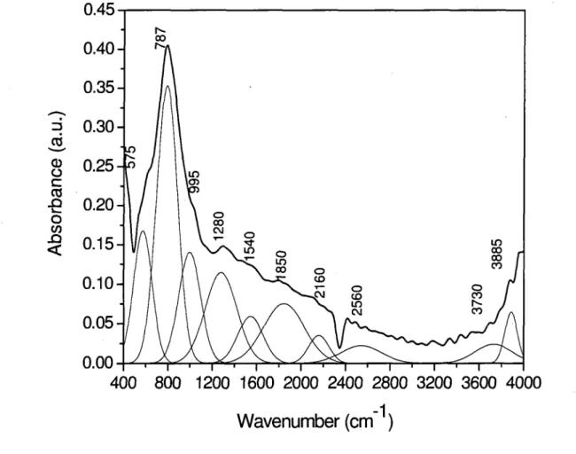
view 31 Figure 2.2: FTIR spectra of SiC thin film and the corresponding deconvolution peaks 33
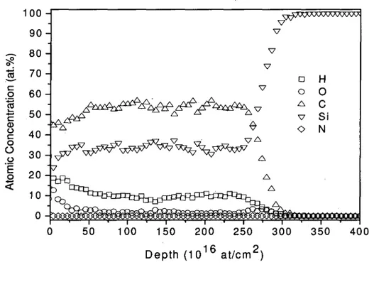
Figure 2.3: TOF-ERD analysis of the atomic depth profile of SiC thin film 35
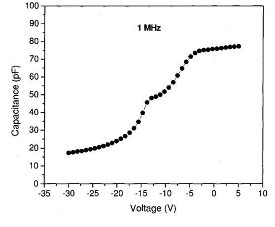
Figure 2.4: High frequency C-V characteristics of SiC/Si structure 36 Figure 2.5: The square-root of the absorption coefficient of SiC thin film as a function of
photon energy. The optical band gap is extracted by extrapolating the linear region of the
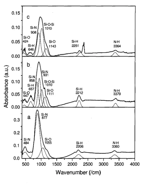
curve as indicated by the dotted line 38 Figure 3.1: FTIR absorption spectrum obtained at a resolution of 4 cm"1 in the wavenumber
range between 400 cm'1 and 4000 cm"1 and the corresponding Gaussians spectral
decomposition; (a) sample SI, (b) sample S2, and (c) sample S3 53 Figure 3.2: Depth profile analysis of the relative atomic concentration of chemical elements
in SiONC thin film obtained by Elastic Recoil Detection (ERD) technique using the upgraded EN-1 HVEC Tandem accelerator at Ecole Polytechnique de Montreal, (a) sample
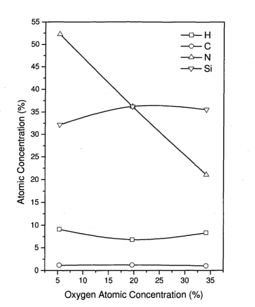
SI. (b) sample S2 and (c) sample S3 55 Figure 3.3: The variation of relative atomic concentration of Silicon. Nitrogen. Carbon and
Hydrogen as a function of the bulk atomic concentration of oxygen in SiONC thin films
based on the results shown in table 3.1 57 Figure 3.4: The X-ray photoelectron spectroscopy analysis of sample S2. The measurements
were performed with MgKa X-ray radiation source at 300 watts. An area with a planar
integration of 2 mm x 3 mm and a depth of 59 Figure 3.5: High resolution X-ray photoelectron spectroscopy peaks analysis and the
corresponding spectral decomposition for sample S2; (a) Silicon, (b) Nitrogen, (c) Carbon, and (d) Oxygen, The spectral decomposition of nitrogen and oxygen spectra showed a single
peak corresponding to Nls and Ols respectively 61 Figure 4.1 : Capacitance-Voltage Characteristics of SiONC/(p)Si MOS structure measured at
1 MHz using an imperdance analyzer equipped with a mercury probe 75 Figure 4.2 : Capacitance-Voltage Characteristics of SiONC/(p)Si MOS structure measured at
10 kHz using an imperdance analyzer equipped with a mercury probe 76
Figure 4.3 : Conductance-Voltage Characteristics of SiONC/(p)Si MOS structure measured
at 1 MHz using an imperdance analyzer equipped with a mercury probe 78 Figure 4.4 : Relative dielectric constant obtained by capacitance-voltage measurement at an
angular frequency of 10 kHz. The refractive index is obtained by ellisometry at a wavelength
of 632.8 nm 80 Figure 4.5 : Square root of the absorption coefficient as a function of incident photon energy
calculated from the absorption spectra, which is obtained using an ultra-violet visible (UV-Vis) photo-spectrometer. The optical bandgap is extracted by extrapolation as indicated by
dotted line in this figure 82 Figure 5.1 : Atomic chemical composition of SiCON thin films obtained by Time-Of-Flight
Elastic Recoil Detection spectroscopy (TOF-ERD), using EN-1 Tandem accelerator. A 40 MeV cobalt ions beam was used for depth profiling of the samples. The graphs correspond to three samples with different atomic concentrations of oxygen: (a) sample SI, (b) sample S2
and(c) sample S3 97 Figure 5.2 : High-frequency capacitance-voltage (C-V) and conductance-voltage (G-V)
characteristics of Mg/SiCON/p-GaAs MOS structure obtained at 1 MHz. The graphs correspond to three samples with different atomic concentrations of oxygen: (a) sample SI,
(b) sample S2 and (c) sample S3 '. 99 Figure 5.3 : Low temperature photoluminescence (PL) spectra acquired before and after the
passivation of p-GaAs using SiCON thin films with different atomic concentrations of oxygen. The PL measurements were carried in vacuum using a 532 nm argon laser source,
with a power of approximately lW/cm2 102
Figure 5.4: Low resolution X-ray photoelectron spectroscopy (XPS) spectrum obtained from the analysis of the interface between SiCON thin films and p-GaAs substrate. The analysis
was performed with Kratos AXIS-HS system using a 120 W MgKa X-ray source 103 Figure 5.5: High resolution X-ray photoelectron spectroscopy (XPS) analysis of As-3d and
Ga-3d peaks, and the corresponding deconvolution peaks, obtained both before and after the
passivation of p-GaAs with SiCON thin films 105 Figure 6.1 : MOS capacitor structure on GaAs substrate with SiCON polymer-based thin film
as a gate dielectric. 119 Figure 6.2 : Capacitance-voltage and conductance-voltage characteristics of SiCON/GaAs
MOS capacitors obtained at 1 MHz after correction for series resistance assuming a parallel capacitance conductance model. The measurements were obtained at different atomic concentrations of oxygen in polymer-based thin films: (a) sample SI, 23 at.%; (b) sample S2,
17 at.%; (c) sample S3, 12 at.%; 122 Figure 6.3: Conductance versus frequency characteristics measured in the depletion region, at
at.%; (b) sample S2, 17 at.%; (c) sample S3, 12 at.%; assuming a parallel capacitance
conductance model 125 Figure 6.4: Current-voltage characteristics of forward and reverse biased SiCON/GaAs MOS
diodes measured at different atomic concentrations of oxygen in polymer-based thin films:
(a) sample SI, 23 at.%; (b) sample S2, 17 at.%; (c) sample S3, 12 at.% 127 Figure 6.5: Linear fitting of the forward and reverse leakage current of SiCON/GaAs MOS
diodes to Frenkel-Poole emission model, obtained at different atomic concentrations of oxygen in polymer-based thin films: (a) sample SI, 23 at.%; (b) sample S2, 17 at.%; (c)
sample S3, 12 at.% 128
LIST OF TABLES
Table 2.1: Absorption peaks assignments of SiC thin film obtained by PS-CVD 34 Table 3.1: Atomic concentration of chemical elements in SiONC thin films extracted from
ERD analysis at a depth of 70 nm which approximately correspond to the average atomic concentration in the bulk of these samples. The table also shows the film thickness measured
by ellipsometry 56 Table 3.2: Relative atomic concentration percentage and identification of chemical bonding
of sample S2 extracted from X-ray photoelectron spectroscopy analysis 60 Table 4.1 : Electrical and optical properties of PS-CVD SiONC thin films obtained for
different atomic concentrations of oxygen 79 Table 5.1: Summary of electrical, optical and chemical properties of SiCON thin films
deposited on GaAs by chemical vapor deposition (CVD) process using a polymeric
precursor 101 Table 6.1 : Summary of the properties of SiCON/GaAs MOS capacitors 129
LIST OF ACRONYMS
ALD APPLD ATM CBE CMOS C-V CVD EBE FET FTIR G-V G-co I-V LPCVD MBE MIS MOCVD MOS OLED OTFT OVPD PDMS PECVD PL PLD PSCVD PTFE SEM SOG SSQ STM TOF-ERD ULSI UV/Vis XPSAtomic layer Deposition
Atmospheric Pressure Plasma Liquid Deposition Atomic Force Microscope
Chemical Beam Epitaxy
Complementary Metal-Oxide-Semiconductor Capacitance-Voltage
Chemical Vapor Deposition Electron Beam Evaporation Filed-Effect-Transistor Fourier Transform Infra-Red Conductance-Voltage
Conductance-Frequency Current-Voltage
Low Pressure Chemical Vapor Deposition Molecular Beam Epitaxy
Metal-Insulator-Semiconductor
Metal Organic Chemical Vapor Deposition Metal-Oxide-Semiconductor
Organic Light Emitting Diode Organic Thin Film Transistor Organic Vapor Phase Deposition Poly-Di-Methyl-Silane
Plasma Enhanced Chemical Vapor Deposition Photoluminescence
Pulsed Laser Deposition
Polymer-Source Chemical Vapor Deposition Teflon
Scanning Electron Microscope Siloxane
Silsesquioxane
Scanning transmission Microscope Time of Flight Elastic Recoil Detection Ultra Large Scale Integration
Ultra-Violet Visible
X-ray Photoelectron spectroscopy
CHAPTER 1
INTRODUCTION
1.1 Semiconductor technology status and trends
During the past few decades, the continuous increase in transistor density and performance guided by CMOS scaling process according to Moore's Law, has been a highly successful methodology in the rapid development of silicon technology. As the silicon industry is moving into the 22 nm node and beyond, significant technological challenges are imposed by silicon CMOS device scaling [1]. Two of the most important challenges are the continuous rising of power dissipation and the increasing variability in device characteristics. As the CMOS devices are approaching quantum-mechanical physics boundaries, it becomes evident that Moore's Law and CMOS scaling are coming to an end [2]. Industry directions for addressing these challenges are developing along two primary axes: extending silicon scaling through innovations in materials and device structure; and exploring post-silicon CMOS technology with new nanodevices based on distinctly different principles of physics, new materials, and new assembly processes.
1.1 Thin film materials technology
microelectronics, optics and nanotechnology, over the past decade. The extension of synthesis flexibility has allowed the design and development of novel materials and precise control of their chemical composition and atomic nanostructure. As a result, a large number of new thin films material and deposition processes have been developed in recent years, which have enabled the fabrication of precisely controlled devices structure. Nowadays, there is now a much greater understanding of the link between film deposition parameters, film structure, and film properties. Such advances in the understanding of thin film preparation has been made possible by the development of broad range of deposition techniques such as molecular beam epitaxy (MBE) [3], atomic layer deposition (ALD) [4] and atmospheric pressure plasma liquid deposition (APPLD) [5], and also through advances in materials in-situ and ex-in-situ characterization tools such scanning tunneling microscope (STM) and atomic force microscope (ATM), to name only a few.
1.2 The nanotechnology era
As we enter the nanotechnology era it is becoming clear that the precise control of the atomic structure of thin film materials will become increasingly important to further the miniaturization of semiconductor devices [6]. The ability to understand and control the structure of materials at the atomic level will be essential if the semiconductor industry is to continue on its historical growth. Today, all the tools required to manipulate and observe the matter at the atomic level are available, and the ability to manipulate atoms at the atomic scale has been recently demonstrated [7]. While constructing a nanostructured block one atom at a time appears to be very attractive process for building nanodevices, it is unlikely that this process will be practical for large scale industrial fabrication of nanodevices, at least
in the near future. In contrast, nano-structured, self-assembled polymer materials, obtained through chemical synthesis, are expected to play a major role in shaping the future of semiconductor devices and nanotechnology [6, 8].
1.2 Polymer-based thin film materials
1.2.1 Brief introduction to polymers
Polymers have traditionally been used in electrical applications as the insulating materials that surround metal wires in order to prevent short-circuit between conductors, primarily because most polymers are electrically insulating. However, Alan J. Heeger, Alan G. MacDiarmid and Hideki Shirakawa (Chemistry Nobel prize laureates in 2000) changed this point of view nearly three decades ago when they observed a tremendous conductivity increase, by a factor of more than one billion, upon chemical oxidation of a polymer known as polyacetylene [9]. The relatively high conductivity observed in this polymer was later attributed to rc-conjugated double bonds [10]. Since then, polymer-based electronic material and devices have quickly evolved into a well-established research and industrial field [11].
Today, there is a huge number of polymer materials available in the market, obtained either through chemical synthesizes or from natural processes [12]. Despite a broad spectrum of chemical structures and material properties possessed by various polymers, they are all built up from nanostructured units which are self-assembled to each other to form a long macromolecular chain upon polymerization. The result is usually an amorphous material that often can be processed from solution into very thin and flexible films by using a wide range of coating and deposition processes. The ability to process the polymers from solutions is a
key factor in manufacturing flexible polymer electronic devices at very low cost [13]. The other most important feature of polymers is the predictable variation of their optical and electronic properties with the molecular mass and chemical structure, which, in conjunction with the progress of the chemical synthesis procedures, have allowed the preparation of novel polymeric materials, with precise properties and functionalities, tailored for a wide range of applications [14].
1.2.2 Organic polymer thin films
Currently, polymer materials have found use in the electronics industry in both manufacturing processes used to generate today's integrated circuits and as component in the device structure [15, 16]. The electronic properties of polymer-based thin films have been the subject of intense research because of the potential application of these materials as alternatives to conventional semiconductors for building low-cost, large area, flexible electronic devices [17].
Today a wide range of semiconductors, dielectrics and conductors based on polymer materials are available, and they have been successfully used to fabricate a growing number of semiconductor devices such as organic thin film transistor (OTFT) [18], organic solar cell [19], organic light emitting diode (OLED) [20], organic nonvolatile memory [21], organic waveguide [22], etc. The majority of these devices are prepared at relatively low temperature and in many cases at room temperature. As a consequence of the bonding structure of active organic materials, the semiconductor devices based on organic polymers have very low performance and are temperature and radiation sensitive, which make them relatively unstable and susceptible to degradation over somewhat short period of time [23].
1.2.3 Inorganic polymer thin Him
In spite of the growing importance of organic polymers, attention is being focused increasingly on polymers that contain inorganic elements as well as organic components [24]. The main reason for the interest in this class of hybrid polymers is that inorganic polymers combine the advantages of inorganic materials and at the same time minimize some of the disadvantages of organic polymers [25]. The organic materials are usually easy to fabricate and process, but they become relatively unstable when exposed to high temperature, strongly oxidizing agents, high energy radiation and high intensity of light [26]. In inorganic polymers, combinations of properties can be achieved and tuned by combining the properties of inorganic backbone and the organic substituent [27]. While the backbone of inorganic polymer provides highly stable polymer structure with superior, mechanical, thermal, chemical and electrical properties, the organic constituents enable the reactive functionalities of the polymer.
Presently, inorganic polymers find application in nearly every industry and in a growing number of commercial products commonly used today. The majority of these applications consist of protective coating and materials reinforcement [28]. In semiconductor industry these polymers are mainly used in devices packaging and as a low-k interlayer dielectric materials in integrated circuits. However, in recent years, several emerging applications are being investigated such as nanolithography, integrated planar waveguide, high-K dielectric for embedded capacitors, etc [29, 30].
organosilane) in particular, are by far the most extensively studied inorganic polymers, due to their unique properties, which cannot be easily matched by other organic polymers [31]. Because of the importance of organosilicon polymers to the work presented in this thesis, further attention will be given to this class of polymers in the following sections.
1.3 Deposition of Polymer-based thin films
A large number of deposition processes have been developed for coating polymer thin film on a variety of substrates. The choice of the most advantageous deposition process for a particular polymer depend greatly on the polymer chemical and physical properties, the deposition temperature and the type of substrates to be coated, in addition to film quality such as uniformity, planarity, and defects concentration. The deposition processes of polymer thin films are broadly classified into two general categories: liquid phase deposition processes and vapor phase deposition processes.
1.3.1 Liquid phase deposition processes
The liquid phase deposition process is a relatively simple and mature process traditionally used for coating decorative materials on a variety of objects. The deposition process is achieved by dipping the object to be coated into a liquid solution of the coating material and then dried naturally or in a furnace to enhance the mechanical strength of the coating material. Today this process has greatly evolved and became a driving technology in polymer industry. A large number of liquid phase deposition techniques of thin films are available today including spin-coating, dip-coating, spray-coating, roll-coating, screen-printing, inkjet-screen-printing, etc [32, 33].
In recent years sol-gel process, which combines liquid phase deposition techniques and polymer materials synthesis, has emerged as a very promising process for the deposition of ceramic thin film materials [34]. The sol-gel process offer many advantages, including low processing temperature, low deposition cost, large area coating, and very low equipments investment, in addition to the availability of unlimited number of pure and stable organic and inorganic materials, which can be easily obtained via chemical synthesis. Currently, the sol-gel process is widely used to prepare polymer-based ceramic thin films materials. The process has also demonstrated its potential towards commercial manufacturing in various fields of applications such as 1OW-K interlayer dielectrics and planar waveguides [35], and it is very promising technology for printed microelectronic devices and for block copolymers self-assembly in future nanoelectronic devices [36].
1.3.2 Vapor phase deposition processes
Vapor phase deposition processes have been widely used in semiconductor industry for several decades as the preferred method for coating the majority of inorganic materials commonly used in the fabrication of integrated circuits. The high quality of the thin films obtained through thermal evaporation in vacuum, and the ability to control precisely the thickness and the roughness of thin films are some of the many advantages offered by vapor phase deposition processes. Today, there are a large number of vapor phase deposition processes, which are widely used semiconductor industry; such as plasma enhanced chemical vapor deposition (PECVD) [37, 38], low pressure chemical vapor deposition (LPCVD) [38], metal organic chemical vapor deposition (MOCVD) [39], molecular beam epitaxy (MBE) [3.
39], Chemical Beam epitaxy (CBE) [39], atomic layer deposition (ALD) [4], and many others.
The majority of polymers thin films can be deposited by liquid phase deposition processes. However, these processes present several problems such as non uniform film thickness, pinholes, non-conformality of the polymeric film to the substrate, as well as the residual solvent in the films [40]. In addition there are many attractive organic and inorganic polymers which cannot be easily dissolved to form a solution. In order to solve these problems and meet the demand for high performance organic polymer devices, several vapor phase deposition processes, adapted for coating polymer thin films materials, have been developed in recent years [41]. These processes have enabled better control of thickness, composition, structure, purity and morphology of polymer thin films. Some of the chemical vapor deposition processes include low pressure organic vapor phase deposition (OVPD) [42], and atmospheric pressure plasma liquid deposition (APPLD) [5]. Polymer thin films have also been obtained by physical vapor deposition of monomers using electron beam evaporation (EBE), sputtering, and pulsed laser deposition (PLD), in the presence of an activating source such as a hot filament or quartz lamps which act as initiators for polymerization [43]. While these depositions methods are widely investigated for the growth of organic polymer, our research have been focused on the development of chemical vapor deposition (CVD) process of inorganic polymer materials, such as polysilanes. Figure 1.1 shows the CVD system setup used in our laboratory for the deposition of polymer-based thin films.
- j . - . *
A \
r/
' f ;;>i
•» \\.\\\\\*HH
"lit
Figure 1.1: Typical setup of the chemical vapour deposition (CVD) system used for the deposition of polymer-based thin films. The top image shows the three-zone furnace with a horizontal quartz tube, and the polymer powder dispensing system. The bottom image shows
1.4 Silicon based polymeric materials
1.4.1 Organosilane polymers
Organosilane (organosilicon) polymers have been known for nearly a century, the interest in these materials is motivated by the abundance of silicon on earth and also the distinctive and superior properties of these inorganic polymers as compared to organic polymers [44]. Organosilane polymers in their broadest definition are defined as polymers with silicon atoms in their backbone. They can only be obtained through chemical synthesis, as they do not occur naturally. Because the silicon can form bonds with most of other elements in the periodic table, this has lead to an explosion in the number of organosilicon polymers available today [31, 44, 45].
Organosilicon polymers can be subdivided into four major categories based on silicon coordination, which include polysiloxanes, polysilazanes, polycarbosilanes, and polysilanes [44, 46]. The global interest in polysiloxanes, polysilazanes, and polycarbosilanes polymers is primarily linked to their wide use in production of ceramic materials, such as silicon carbide, silicon nitride and silicon dioxide, which are commonly used for protective coatings, insulation, and reinforcement of nanocomposite materials [47]. The polysilanes on the other hand started to emerge in recent years as a potential material, which is very promising as a dielectric, semiconductor, and conductor in various applications [46-48]. As a result, the following sections will be mainly focused on polysilanes polymers.
1.4.2 Polysilane polymers
Polysilane polymers also called polysilylene, have received much attention in recent years because of their unusual electric and photoelectronic properties. The distinctive properties of these polymers were attributed to the derealization of the a-electron along the Si-Si backbone chain [48, 49]. The electrical and optical properties of polysilanes differ significantly from structurally analogous carbon-based a-bound systems, like polystyrene and polyethylene, and rather resemble fully 7t-conjugated systems, like poly acetylenes. While polysilanes, in general, exhibit dielectric behavior, they can be made semiconductor with the addition of suitable dopants such as FeCl3, SbFs or iodine (I2) [50]. The conductivity of the
i c 'a 1
polymer can be modulated in the range 10" to 10' S cm" through a combination of organic substituents and dopants. The ability to modulate the conductivity of polysilanes over a broad range have made them very attractive both as a dielectric and as a semiconductor in a wide range of microelectronic and optoelectronic applications such as solar cells [51], light emitting diodes [52], integrated waveguides [53] and phototransistors [54].
1.5 Preparation of polysilanes polymer-based thin film
1.5.1 Synthesis and functionalization of polysilanes
Polysilanes have been widely prepared by the classic Wurtz-type coupling reaction of dichlorosilanes with its typical conditions of molten sodium in hot toluene [46]. However this preparation method is not convenient for incorporating many functional groups in polysilanes polymers. As a consequence, a number of new routes suitable for the synthesis of polysilanes, which allow more diversified functional groups and enable the control of the
polymer structure at the micro and macro level, have been developed. Some of these synthesis routes include anionic polymerization of masked disilenes, ring opening polymerization, dehydrocoupling polymerization, electrochemical polymerization, chemical vapor deposition polymerization, redistribution polymerization and disproportionation polymerization [46, 55].
The modification of the physical and chemical properties of the polysilanes polymers can be achieved through pre- and post-polymerization functionalization [56, 57]. The combination between the different synthesis routes and the functionalization processes, discussed above, provide unlimited possibilities to design and tune the properties of polysilanes polymers to satisfy the requirements of future microelectronic and nanoelectronic materials and devices.
1.5.2 Chemical vapor deposition of polysilanes thin films
The conventional method commonly utilised to prepare polysilanes based polymers films consist of dissolving a polymer precursor in an organic solvent to obtain a liquid solution with the required viscosity. The solution is then spin coated on the substrate and pyrolyzed at high temperature in oxygen-free atmosphere in order to evaporate the solvent. This method of preparation has been broadly used for ceramic coating and preparation of dielectric materials [58, 59]. The poor quality of polymer thin films obtained by this method and their porous nature and also the non availability of solvent for many polysilanes polymers such as polydimethylsilane (PDMS), have considerably limited the applications of polysilanes polymers.
Due to many attractive properties of polysilanes, they are very promising for wide range of nanoelectronic and nanophotonic applications. However, many of the new emerging applications require precise control of thin films thickness, morphology, atomic composition, and chemical structure which cannot be achieved by spin coating process. Therefore, over the past few years our research group have been focusing on the development of polymer-based chemical vapor deposition process of polysilanes materials [60, 61]. This process is expected to enable the growth of high quality thin film with a wide range of properties that can be easily customised through polymer synthesis and functionalization. One of the main objectives of this Ph.D. thesis is to design and optimize the chemical vapor deposition system and the deposition process of polysilanes polymer-based thin film and to explore their potential applications.
1.6 Polysilanes polymer-based thin films potential applications
In recent years a growing number of promising applications based on of polysilanes are under development. In the following section we will briefly present some of the most important and potential applications of polysilane polymers, which will be further investigated throughout this thesis.
1.6.1
LOW-Kdielectrics materials
As the interlayer spacing in advanced integrated circuit manufacturing is continuously shrinking, 1OW-K dielectric materials are needed to reduce the interlayer dielectric capacitance, in order to minimize the interconnect propagation delay, cross talk noise and power dissipation [62]. In recent years, several spin coated organic and inorganic materials
with very low dielectric constant have been considered as an alternative to SiC>2 in the fabrication of CMOS devices, such as silsesquioxane (SSQ), siloxane (SOG), teflon (PTFE) and polyimides [62, 63]. While materials with dielectric constant values below 3 have been demonstrated, most of them are either not stable at processing temperature above 400 °C or are mechanically weak, and present integration challenges with Cu damascene processes. In order to solve these issues, several 1OW-K dielectric materials obtained by CVD have been recently investigated. Some of the most promising materials include hydrogenated amorphous silicon oxycarbide [64], parylene [65] and fluorinated amorphous carbon [66]. Silicon oxycarbide thin films are widely obtained by CVD using dimethylsilane, trimethylsilanes and tetramethylsilanes as a source material [67]. Polysilanes polymers are very promising alternative to methylsilane molecules as a source material in CVD process. The ability to tune polysilanes polymers through polymer synthesis and functionalization is expected to enable the development of very 1OW-K dielectric materials.
1.6.2 High-K dielectrics materials
The further increase of computing speed is a very difficult and complex problem, which includes the use of new materials, novel electronic devices, and maybe novel principles of computing and computer architecture. As we move toward nanodevices it is becoming obvious that the silicon CMOS technology is facing a very doubtful future. The scaling of conventional silicon based metal-oxide-semiconductor (MOS) transistors will soon require very thin gate dielectric films, below 1 nm. However, the increase of leakage current through thinner Si02 films puts a fundamental limit on the existing MOS technology [68].
High dielectric constant materials are therefore needed in order to reduce the MOS transistor gate leakage current and improve its performance.
In hope to extend the lifetime of Silicon CMOS technology for at least one or two more decades, a large number of new high-K dielectric materials have been investigated as substitutes for SiC«2 in MOS devices, some of these high-K dielectric materials include SiON, AI2O3, Hf02, TaaOs, Zr02, Ti02 and La203 [69-70]. Significant progress has been achieved in the growth processes of these materials and in understanding their chemical, structural and electrical properties, as well as their integration into CMOS devices. After nearly a decade of intense research, the family of hafnium-oxide-based materials, such as Hf02, and HfSi^OyNz, has emerged as a leading candidate to replace Si02 gate dielectrics in advanced CMOS ULSI devices [71]. While hafnium-oxide based high-k dielectrics will probably remain attractive down to 32 nm node, a new high-k dielectric materials will be again required for 22 nm node and beyond.
Hybrid organic-inorganic polymer materials are expected to play a major role in the design of future high-K dielectric materials. Several composite polymer materials with ultra high dielectric constant exceeding 100 have been reported in recent years [73, 74]. Although these materials are still not suitable for MOS application, their development has stimulated interest in the synthesis of new polymers with ultra-high dielectric constant for a wide range of application.
1.6.3 MOSFET passivation
obvious functional advantages of III-V semiconductor devices, 95% of the microelectronics market remains dominated by silicon technology. This is mainly attributed to the high quality of the interface between crystalline silicon and thermally grown silicon dioxide. However, as the silicon technology approach its limits, a shift towards III-V compounds semiconductor materials or other high mobility semiconductor materials will be inevitable in the near future [75]. As a result, research has intensified in recent years in order to identify the most promising high mobility channel materials as a substitute to silicon in CMOS technology, beyond the 22 nm node. Currently, compound semiconductors such as GaAs, InAs and InSb are receiving a great deal of attention as the most attractive high mobility materials for next generation MOSFET [76, 77].
The development of stable gate dielectric material for III-V compound semiconductors, which can achieve very low density of interface defects, comparable with that of silicon dioxide on silicon, remain one of the big hurdles facing the integration and the wide adoption of very high mobility materials. In recent years, tremendous efforts have been made to develop new passivation processes and new nanostructured materials, which have allowed better control and understanding of surface and interface properties of various dielectric thin films on III-V compound semiconductor [78, 79]. As a result, it is becoming clear that precise control of the atomic composition and the molecular structure of the passivation layer are very critical in order to achieve excellent passivation of high mobility compound semiconductors. Therefore, synthetic polymer materials with precise atomic configuration and chemical composition are expected to play a key role in the development of new passivation materials for high mobility compound semiconductor in future CMOS technology. Currently, organosilanes polymers such as polysilanes are starting to attract a lot
of attention as a source material in wide range of surface passivation and surface functionalization processes [80]. The ability to tailor atomic composition and chemical structure of these polymers, via chemical synthesis and functionalization, make them very promising for passivation of high mobility compound semiconductors.
1.6.4 Silicon carbide
Silicon carbide (SiC) based semiconductor electronic devices and circuits are presently being developed for use in high-temperature, high-power, and high-radiation conditions under which conventional semiconductor materials cannot adequately perform [81]. Silicon carbide's ability to function under such extreme conditions is expected to enable significant improvements in the performance of a variety of applications such as high-voltage switching, electric motor drives, and more powerful high speed communications systems. Silicon carbide exhibits many superior properties, such as high thermal conductivity (4.9 W/cmK), relatively high electron mobility (1000 cm2/Vs), high breakdown electric fields (4
x 106 V/cm), wide bandgap (2 to 3.5 eV), and excellent physical and chemical stability.
These characteristics make this material the ideal choice for high temperature, high power, and high voltage integrated electronic devices such as power MOSFET and rectifying diodes [82, 83]. The biggest problem with the commercialization of SiC devices is the high cost and limited availability of bulk substrate. Although 6H-SiC and 4H-SiC bulk substrates are now available from few suppliers, the wafers quality is still far from optimized. As a result, a lot of works have been focused on the development of high quality silicon carbide thin films on various substrates.
Chemical vapor deposition (CVD) is widely employed for epitaxial growth silicon carbide (P-SiC) thin films on crystalline silicon substrate. Highly crystalline P-SiC thin films are normally obtained at relatively high temperature, around 1300 °C, using a combination of gases precursors such as silane and hydrocarbons [84]. High growth temperatures usually result in high tensile stress and lattice defects in silicon carbide thin films, due to the differences in lattice constants and thermal expansion coefficients between silicon carbide and silicon. Furthermore, the very high deposition temperature makes the integration of silicon carbide thin film difficult and incompatible with many applications and fabrication processes.
In attempt to reduce the deposition temperature of p-SiC thin film, efforts have been focused in recent years on the synthesis of new precursor materials. Single source precursors of organosilanes molecules such as tetramethylsilane, trimethylsilane, dimethylsilane, monomethylsilane, and disilabutane have been extensively investigated, as an alternative to conventional silane and methane gases mixture in CVD process [85]. Ceramic SiC thin film is also widely prepared via spin coating and pyrolysis of organosilanes polymers such as polysilanes and polycarbosilanes [86].
In recent years, our research group has been focused on development of new CVD process for the deposition of ceramic silicon carbide thin film using polysilanes polymers as source materials [61]. This new approach has many advantages such as high deposition rate, hazard free environment; due to elimination of gases precursors, compatibility with batch processes, and overall low deposition cost of ceramic SiC thin films.
1.6.5 Integrated optical waveguides
The rapid growth of telecommunication market increasingly demands high speed processing and transmission of large-bandwidth data. In order to satisfy these demands, highly integrated low cost optical and photonic devices are required. During the last two decades, attention has been paid to silicon oxynitride (SiOxNy) as a potential material for planar integrated optics [87]. This attention has been mainly motivated by its excellent optical properties such as low absorption losses in the visible and near infrared. SiON combines the dielectric properties of SiC>2 together with good chemical inertness and low permeability of Si3N4. In addition, the refractive index of SiON thin film can be easily adjusted over a wide range (1.45 to 2.0) by simply varying the concentration of oxygen in the film [88]. This attractive property allows fabrication of waveguides with desired characteristics of fiber match and compactness. Moreover, the growth of SiON layers on silicon substrate is done by well established standard silicon integrated circuit fabrication processes, which enable low cost and high integration of planar waveguides and several other optical devices.
Silicon oxynitride thin films are widely deposited by plasma enhanced chemical vapor deposition (PECVD) [88-90] and low pressure chemical vapor deposition (LPCVD) [90] using a mixture of gases precursor such as silane (SiFLO, ammonia (NH3) and nitrous oxide (N2O). SiON can also be prepared by several other CVD methods using a wide range of organosilanes molecules and polymers as a source material. Currently, polymer-based thin films materials, and particularly polysilanes are attracting a lot of attention as a low cost alternative for the fabrication of integrated optical waveguides [91, 92]. The discovery of photobleaching phenomenon in conjugated polymers has made polysilanes very promising
for the design and the fabrication of very complex planar waveguide structures for optical communication [93].
CHAPTER 2
CHARACTERIZATION OF SILICON CARBIDE THIN FILMS OBTAINED VIA SUBLIMATION OF A SOLID POLYMER SOURCE USING POLYMER-SOURCE
CVD PROCESS
CARACTERISATION DES COUCHES MINCES DE CARBURE DE SILICIUM OBTENUES PAR SUBLIMATION D'UNE SOURCE POLYMERIQUE SOLIDE EN
UTILISANT UN PROCEDE CVD
Materials Research Society (MRS) Proceedings, vol. 989-A5-5 (2007)
El Hassane Oulachgar1, Cetin Aktik1, Starr Dostie2, Subhash Gujrathi3 and Mihai Scarlete2 1 Nanofabrication and Nanocharacterization Research Center (CRN2)
Department of Electrical and Computer Engineering, Sherbrooke University
2 Thin Film Research Laboratory (TFRL)
Department of Chemistry, Bishop's University
3 Thin Film Physics and Technology Research Center (GCM)
Abstract
Silicon carbide thin films have been deposited via sublimation of a solid organosilane polymer source using atmospheric pressure chemical vapour deposition process (PS-CVD). The advantages of this new process include high deposition rate, compatibility with batch process, hazard-free working environment and low deposition cost. The silicon carbide (SiC) thin films obtained through this process exhibit a highly uniform film thickness, highly conformal coating, and very high chemical resistance to acids and alkaline solutions. These characteristics make the SiC thin films obtained by PSCVD process very attractive as a structural material for micro-electro-mechanical systems (MEMS) and as a coating film in a wide range of other applications. These SiC thin films are also expected to be attractive as a semiconductor material provided that the defects, oxygen and nitrogen contaminations can be reduced and effectively controlled. In this work we have investigated the chemical, structural, electrical and optical properties of these films, using scanning electron microscope (SEM), Fourier transform infrared spectroscopy (FT-IR), elastic recoil detection spectroscopy (ERD), ultraviolet-visible photospectroscopy (UV-Vis), ellipsometry, and capacitance-voltage measurements (C-V).
Resume
Les couches minces de carbure de silicium ont ete deposees par sublimation d'une source de polymere solide d'organosilane en utilisant un procede de depot en phase vapeur, a pression atmospherique (PS-CVD). Ce nouveau procede a plusieurs avantages en particulier un taux de deposition tres eleve, la compatibilite avec le traitement par lots, un environnement de travail sans risque et un coiit de deposition relativement bas. Les couches minces de carbure de silicium (SiC) obtenues par ce procede ont une epaisseur tres uniforme, un revetement conforme et une forte resistance chimique aux solutions acides et alcalines. Ces caracteristiques rendent les couches minces de SiC obtenues par le procede de PSCVD tres attrayantes comme un materiau de structure pour les systemes micro-electro-mecaniques (MEMS) et comme une couche de revetement pour un large eventail d'applications. Ces couches minces de SiC pourraient etre egalement interessantes comme materiau semiconducteur a condition que les defauts, et les contaminations d'oxygene et d'azote puissent etre reduites et efficacement controlees. Dans ce travail nous avons etudie les proprietes de produit chimique, structurales, electriques et optiques des couches minces de SiC obtenues par le procede PS-CVD en utilisant le microscope electronique a balayage (SEM), la spectroscopie infrarouge a transformee de Fourier (FT-IR), la spectroscopic elastique de detection de recul (ERD), la photospectroscopie ultra-violet-visible (UV-Vis), l'ellipsometrie, et la mesure de capacite-tension (C-V).
2.1 Introduction
Thin films of silicon carbide have been intensively investigated as an alternative to crystalline silicon carbide mainly because of their low preparation cost, simple processing and easy integration with other thin film materials. Nowadays they are commonly used in a wide range of semiconductor devices including window layer for solar cells [1], rectifying diode [2], photo-detector [3], MEMS pressure sensor [4], surface coating [5], membrane for X-ray lithography [6] and a variety of other applications.
Chemical vapour deposition (CVD) process has been widely used in semiconductor industry for several decades and it is commonly used to prepare both crystalline and amorphous thin films of silicon carbide [7-12]. However, high quality single crystal silicon carbide are usually obtained with this process at very high temperature. In recent years, thin film of 3C-SiC epitaxially grown on silicon at a relatively low temperature (800 °C -1300 °C) are being widely investigated as a promising alternative to bulk crystalline silicon carbide [8, 12]. However, these films can only be grown on silicon wafer and a carbonisation process is always required, to minimize film stress and to achieve epitaxial growth. Because the CVD process requires highly volatile precursors to achieve uniform and continuous vapour transport, the majority of CVD processes are designed for the utilization of gaseous or liquid sources with high vapour pressure at specific temperature. Most of these gases precursors are highly toxic, oxygen and moisture sensitive, and highly flammable, so that special handling precautions are always required.
Amorphous, nanocrystalline and polycrystalline silicon carbide films have been deposited as the ceramic residue obtained via spin-coating or dip-coating of various liquid and solid polymeric precursors, such as polycarbosilane or organo-polysilane species [13-16]. In contrast with the CVD process, the low volatility is a crucial property for the polymeric precursors in order to achieve a high ceramic yield. These silicon carbide ceramic films are sought due to their valuable intrinsic properties such as high tensile strength, high thermal conductivity and radiation resistance, and rarely for their electrical properties. Currently, many efforts are dedicated to the synthesis of high purity polymeric precursor, and to develop new methods for the deposition of silicon carbide thin films better adapted to the chemical and structural purity required by the semiconductor industry.
A CVD process using a polymeric source appeared to be an attractive method to deposit silicon carbide thin films at a relatively lower temperature and at a lower cost [17]. This idea has been rapidly accepted by various academic research groups and industrial players, covering the whole chart between fundamental research and new emerging commercial products. Currently, a handful of important players are in competition either for the design of various polymeric sources adapted to different applications, or for the optimization of CVD-parameters adapted to the utilization of polymeric sources. In this paper we present and discuss the chemical, electrical and optical characteristics of SiC thin films obtained by this method using polydimethylsilane (PDMS) solid polymer source.
2.2 Experimental
Silicon carbide thin films were obtained through the sublimation of polydimethylsilane (PDMS) polymer powder using Lindberg horizontal three-zone furnace.
The furnace is equipped with a 2.5 inch quartz tube attached to an argon tank, an oil bubbler, and a Fisher Maxima vacuum pump capable of achieving a vacuum down to 103 torr. The
films were deposited on both polished N-type crystalline silicon wafer and on electronic grade quartz substrates. Prior to deposition of SiC thin films, silicon and quartz substrates were properly cleaned in an ultrasonic bath for several minutes using acetone, isopropyl alcohol (IPA) and deionized-water, and were dried using boiling isopropyl alcohol. The samples were introduced in the furnace together with a boat containing the PDMS polymer powder. In order to eliminate residual moisture and oxygen contamination, the reactor is pumped down for extended period of time and purged three times with the flow of ultra high purity argon before starting the polymer sublimation process. Argon was used as the carrier gas, with a constant flow during the deposition process. The deposition pressure is kept near atmospheric pressure while the deposition temperature is gradually increased up to 800 °C at a rate of 16 °C per minute. The samples were maintained at the maximum temperature for approximately 30 minutes, immediately after that the reactor is shut down to allow natural cooling of the samples, to avoid film cracking.
Fourier transform infrared spectroscopy (FT-IR) has been used to examine the deposited film on single crystal silicon wafers. The absorption spectra were acquired in the MID-IR range (4000 cm"1 to 400 cm"1), using a Mattson Galaxy Series FTIR-6020
spectrophotometer. The atomic composition of the films was obtained by elastic recoil detection spectroscopy, using time-of-flight analysis (TOF-ERD). The films morphology was analyzed using high resolution scanning electron microscope (SEM). The dielectric constant was extracted from capacitance-voltage measurement obtained by Schlumberger impedance analyzer SI260 equipped with a mercury probe. The optical band gap was extracted from the
ultraviolet-visible absorption spectra measured using Hewlet-Packard HP8452 UV/Vis spectrophotometer. The films thickness and the refractive index were determined by J. A. Woollam Alpha-SE ellipsometer.
2.3 Results and discussion
2.3.1 Scanning electron microscope (SEM) analysis
The thin films obtained by polymer sources CVD process using PDMS powder are found to exhibit a very uniform film thickness over a relatively large area. Figure 2.1(a) show the cross section image of the film deposited on silicon substrate obtained by scanning electron microscope (SEM). Since the process is not conducted under continuous flow of polymer it was not possible to determine a deposition rate. Because the deposition process is conducted at near atmospheric pressure all the film obtained by this process are conformal; this is confirmed by the SEM cross section image of figure 2.1(c), which shows the deposition of the film on the edge of the wafer. The top view SEM image of the film obtained at high resolution shows very uniform film morphology with very small grain size, which suggests that these films are amorphous. The atomic concentration of oxygen in the samples was found to vary from sample to sample (from 2 at.% to 10 at.%) due to reactor leakage and residual contamination [18]. In this study we only focus on the samples with a low oxygen concentration (around 2 at.%).
M
^ • , ^ J4 ^ *_ V i.» *-^ •"" ~" \ * ^ \. a ~ \ ^ ,_ v« \ *• \\ 1 \ \ \ \ t « » \ », » ' » » < ( 1 ' v > » • * \ \ x \ Hi v ^ i •• , ^ \ 1\ \ \ \ \ ,t V v * \ ^\X\ v \W \\ \ \ \ ^ v \ V \ \ \ » V \\\ \\\ * \ , \ \\» \ v\<s \ \ » ^> \\\imm ®Msmm s3D®.@k @E(M) 0 0 8 6 0 tt a \ JLyO 4 * «\
Figmure 2„ls High-resolution SEM of SiC film on silicon; (a, c) cross section view, (b) top view
2.3.2 Wet chemical etching analysis
The chemical resistance to acid and alkaline solutions was investigated by dipping a silicon substrate coated with 200 nm thick films in both HNA (C202H4:HN03:HF; 8:3:1) and
molten KOH (30 %, 95 °C) solutions for 24 hours. During this experiment, the back sides of the silicon substrates were coated with polyimide and copper foil respectively. After this period of exposure, the film thickness was measured again by ellipsometry and did not show any noticeable change, which indicates that the etch rate in these solutions is extremely slow. These films are therefore highly resistant to both acids and alkaline solutions. The above characteristics make these films very attractive as a coating material and possibly as a thin film membrane for MEMS devices.
2.3.3 Fourier transform infrared spectroscopy (FT-IR) analysis
Immediately after the films deposition the chemical structure was analyzed using FT-IR spectroscopy. Figure 2.2 show the typical absorbance spectrum of the thin films deposited on silicon substrate under the experimental conditions described above. A preliminary look at the FT-IR spectrum shows a main peak around 780 cm"1 commonly associated with silicon
carbide formation [16, 17, 19, 20]. The broad shoulder around 1250 cm"1 is generally
associated with the bending mode of residual Si-Ctb groups in silicon carbide thin film [16, 19, 20].
In order to better understand the structural composition of these films, we further analyzed their spectral decomposition using Peakfit software. The deconvolution of the FT-IR spectra was obtained assuming a Gaussian distribution. The deconvolution reveals several