HAL Id: ujm-00699618
https://hal-ujm.archives-ouvertes.fr/ujm-00699618
Submitted on 21 May 2012
HAL is a multi-disciplinary open access
archive for the deposit and dissemination of
sci-entific research documents, whether they are
pub-lished or not. The documents may come from
teaching and research institutions in France or
abroad, or from public or private research centers.
L’archive ouverte pluridisciplinaire HAL, est
destinée au dépôt et à la diffusion de documents
scientifiques de niveau recherche, publiés ou non,
émanant des établissements d’enseignement et de
recherche français ou étrangers, des laboratoires
publics ou privés.
Contactless Electromagnetic Active Attack on Ring
Oscillator Based True Random Number Generator
Pierre Bayon, Lilian Bossuet, Alain Aubert, Viktor Fischer, François
Poucheret, Bruno Robisson, Philippe Maurine
To cite this version:
Pierre Bayon, Lilian Bossuet, Alain Aubert, Viktor Fischer, François Poucheret, et al.. Contactless
Electromagnetic Active Attack on Ring Oscillator Based True Random Number Generator. COSADE:
Constructive Side-Channel Analysis and Secure Design, May 2012, Darmstadt, Germany. pp.151-166,
�10.1007/978-3-642-29912-4_12�. �ujm-00699618�
France
2
University of Montpellier 2, LIRMM Laboratory, CRNS 5506, 34000, Montpellier, France
3
CEA-LETI, SESAM Laboratory, Centre Micro´electronique de Provence, 13541, Gardanne, France
Abstract. True random number generators (TRNGs) are ubiquitous in data security as one of basic cryptographic primitives. They are primar-ily used as generators of confidential keys, to initialize vectors, to pad values, but also as random masks generators in some side channel attacks countermeasures. As such, they must have good statistical properties, be unpredictable and robust against attacks. This paper presents a contact-less and local active attack on ring oscillators (ROs) based TRNGs using electromagnetic fields. Experiments show that in a TRNG featuring fifty ROs, the impact of a local electromagnetic emanation on the ROs is so strong, that it is possible to lock them on the injected signal and thus to control the monobit bias of the TRNG output even when low power elec-tromagnetic fields are exploited. These results confirm practically that the electromagnetic waves used for harmonic signal injection may rep-resent a serious security threat for secure circuits that embed RO-based TRNG.
Keywords: Active attacks, EM injections, IEMI, Ring oscillators,TRNGs
1
Introduction
True random number generators (TRNGs) are essential in data security hard-ware. They are implemented to generate random streams of bits used in cryp-tographic systems as confidential keys or random masks, to initialize vectors, or to pad values. If an adversary is able to change the behavior of the generator (for instance if he can change the bias of the generated stream of bits), he can reduce the security of the whole cryptographic system.
Surprisingly, there are not many papers dealing with physical attacks on ran-dom number generators. The only practical attack to the best of our knowledge, was published by Markettos and Moore [1]. In their attack, the attacker targets a two ring oscillator (RO) based TRNG implemented in a security dedicated
Integrated Circuit (IC). Markettos and Moore inject a sine wave signal onto the power pad of the device in order to intentionally modify the operating conditions of the two ROs and thus to get a biased output signal.
Within this context, our main contribution is an electromagnetic (EM) attack on the RO based TRNG that can be seen as a significant improvement of the attack introduced in [1]. In our attack, the attacker alters the entropy extractor by injecting an EM signal into the device rather than by inducing a harmonic signal on the power pad.
The EM injection is contactless and does not require any access to the power line. The procedure may be applied to ROs operating at higher frequencies than the cut-off frequencies of the power pad and the supply/ground network. Unlike in [1], the proposed attack may work on generators featuring separated power and ground nets for each RO. Note that this technique is used sometimes in order to decouple the ROs and thus to maximize the entropy per bit at the generator’s output.
In real cryptographic devices, the embedded TRNG is often built using more than two ROs (a 2-RO TRNG targeted in [1] is rather exceptional). For this reason, the EM attacks presented in this paper are evaluated on a TRNG using as much as 50 ROs. This kind of TRNG was considered to be invulnerable up to now.
The paper is organized as follows. Section II presents the TRNG threat model and the general structure of the generator based on ROs studied in the paper. In Section III, the whole experimental platform required for the EM injection attack is detailed. Section IV provides experimental results demonstrating the influence of the EM injection on the ROs. Section V shows how the mono-bit bias of a 50-RO TRNG can be dynamically controlled.
2
Background
This section discusses the TRNG threats and describes briefly the generator adopted as a design under test (DUT) in the rest of the paper.
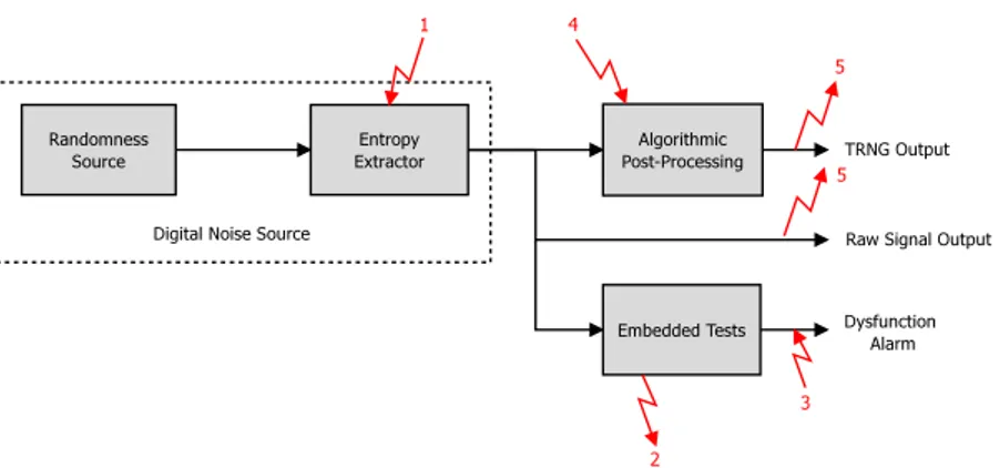
The general structure of a TRNG is depicted in Figure 1. The generator is composed of:
– A digital noise source (randomness source + entropy extractor) that should give as much entropy per bit as possible, enable a sufficient bit-rate and be robust to environmental (voltage, temperature) variations.
– An algorithmic post-processing could be added at the output of the TRNG to enhance statistical properties without reducing the entropy.
– In some cases, the designer could add some embedded tests to evaluate on-chip the quality of the randomness source in real time or to detect online the generator’s permanent or temporal failure. However, advanced and complex statistical tests are time and energy consuming. Therefore, the functionality and the quality of a TRNG can only be periodically tested on-chip.
Fig. 1. Passive (2, 5) and active (1, 3, 4) attacks on a TRNG general structure
2.1 TRNG Threat Model
Two types of attacks on TRNGs can be considered: passive and active attacks. Passive attacks collect some information about the generator in order to predict future values with a non negligible probability (attacks 2 and 5 in Figure 1 – see arrow orientation). Active attacks tend to modify the behavior of the generator in order to control somehow its output (attacks 1, 3, and 4 in Figure 1). According to Figure 1, the adversary may target different parts of the TRNG in different ways. We could expect, that the statistical tests (simple embedded tests or complex external tests) could detect the attack. One could also argue that the algorithmic postprocessing would reduce the force of the attack. However, algorithmic post-processing is missing in some generators [2] or embedded tests are not used, because the generator is ”provably secure” [3]. Nevertheless, it is a common practice in applied cryptography that the security of all building elements is evaluated separately. For this reason, evaluation of the robustness of the generator and all its parts is of great interest.
Many sources of randomness such as thermal noise, 1/f noise, shot noise or metastability can be used in TRNGs. A good source of randomness should not be manipulable (and therefore not attackable) or the manipulation should be prevented. For example, the thermal noise quality can be guaranteed by controlling the temperature. It is thus reasonable to expect that attacks will not target the source of randomness.
In this paper, we will consider attacks on entropy extraction (1). Their objec-tive can be to bias the generator output or to reduce the digital noise entropy, since both bias and entropy reduction can simplify the subsequent attack on the cryptographic system, since the exhaustive key search can be significantly shortened. We will not consider other attacks from Figure 1, such as attacks on tests (2 and 3) and postprocessing (4), because of huge number of methods and cases that should be considered. It is up to the designer, to adapt postprocessing and embedded tests to weaknesses of the generator. The aim of this paper is to
show one of possible weaknesses that could be targeted by attacker in RO-based TRNGs.
As discussed in the introduction, the only published paper dealing with a practical active attack on TRNG is from Markettos and Moore [1]. This paper deals with a harmonic signal injection into the power line of a TRNG based on ROs. The authors claim that they could reduce the digital noise entropy when the frequency of the harmonic signal was close to the frequency of ROs. Their study can be seen as a proof of concept of an attack on TRNG using harmonic injection. Nevertheless, this attack has some practical limits. For example, the attack could be probably countered by separating power and ground lines of all ROs, filtering the power supply, avoiding the access to power line, etc. It is clear, that the efficiency of the attack would be better if it was contactless and undetectable by embedded sensors, such as light sensor.
In this paper, we show that EM waves are good candidates for performing contactless attacks.
2.2 RO-based TRNG
A jittery clock generated by a RO is the most common type of source of random-ness used in TRNGs. ROs are easy to implement in both ASICs and FPGAs. Commonly used TRNG principle employing several ROs was proposed in [3] and enhanced in [2]. The resulting architecture shown in Figure 2 represents one of the simplest TRNG structures that can be implemented in FPGAs. It needs only NOT gates (for implementing ROs), flip-flops (as samplers) and a large XOR gate (entropy collector). In [3], authors proposed a mathematical model of the TRNG that guarantees enough entropy in the output bit and thus the robustness and security. In their model, ROs are assumed to be independent.
The generator has several parameters that can be tuned: number of elements composing ROs, number of ROs and the sampling frequency. Modifying these parameters, the designer can change the statistical properties of the random stream of bit produced by the TRNG. For example, according to [2], for a sam-pling frequency of 100 MHz, the generator composed of 25 ROs, each using 3 NOT gates, generates stream of bits passing the NIST and DIEHARD tests even without post-processing (in the original Sunar’s design [3], the post-processing was mandatory).
3
Experimental Setup
3.1 TRNG Implementation
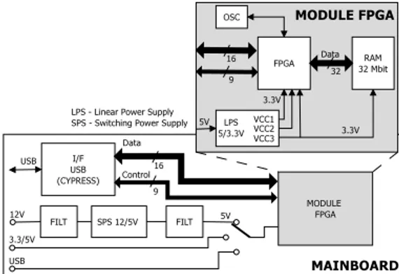
The EM attacks were realized on a board featuring ACTEL Fusion FPGA. The board is dedicated to evaluation of TRNGs. Special attention was payed to the power supply design using low noise linear regulators and to the design of power and ground planes. It is important to stress that the board was not specially designed to make the EM fault injection or side-channel attacks easier, as it is
Fig. 2. RO-based TRNG.
the case of the SASEBO board [4]. It can be seen in Figure 3, that the FPGA module was plugged into the motherboard containing power regulator and USB interface.
Fig. 3. Block diagram of the board dedicated to TRNG testing
In order to demonstrate that the EM injection can disturb both RO and TRNG behavior, we performed attacks on two kinds of implementations:
– The first one was composed of four 3-element ROs. It was aimed at the measurement of the phase difference between four generated clocks (see Fig-ure 4). This implementation will be called Target#1.
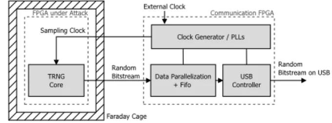
– In the second implementation depicted in Figure 5, the TRNG core was implemented in an FPGA board under attack. Another board that was pro-tected from EM emanations, generated reference clock signals, read data from TRNG and communicated with computer. We decided to separate the communication from random data generation in order to be sure that it was the TRNG that was faulty, not the communication. The communication module is composed of a serial to parallel converter, a FIFO and a USB con-troller. USB interface throughput (up to 20 MB/s) was sufficient to handle the bit rate of the TRNG. The FIFO guarantees that no data are lost during
Fig. 4. Implementation for the measurement on ROs - Target#1
the transfer. Two signals were exchanged between the boards: a clock signal coming from the communication board and the random bitstream produced by the TRNG inside the FPGA under attack. These two signals were mon-itored with an oscilloscope during the attack in order to ensure that their integrities were untouched. This implementation is called Target#2.
Fig. 5. TRNG testing architecture - Target#2
We ensured that the ROs were not initially locked due to their placement. In the rest of the paper, the term ”locked” has the same meaning as in phase-locked-loops (PLL).
In both cases, ROs were composed of three inverters (NOT gates), giving the working frequencies of about 330 MHz. For Target#2, the TRNG was composed of 50 ROs. A sampling clock of 24 KHz was generated in an embedded PLL. This sampling frequency was chosen in order to make a 2-RO TRNG pass the NIST statistical tests. In general, decreasing the speed of the sampling clock will improve the behavior of the TRNG (the jitter accumulation time will be longer). Moreover, we used more ROs than Wold and Tan in [2] (50 versus 25). We stress that the TRNG featuring 50 ROs should pass FIPS, and NIST statistical tests under normal conditions without any problems.
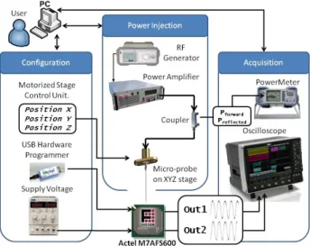
3.2 EM Injection Platform
The EM injection platform is presented in Figure 6. The platform embeds a power injection chain supplying the micro-antenna, but also two other chains:
ized stages,
– collects data provided by the power meter, connected to a bi-directional coupler, in order to monitor the forward (Pforward) and reflected (Preflected)
powers,
– sends configuration data to the ACTEL Fusion FPGA and supplies target boards via USB,
– stores the time domain traces of all signals of interest acquired using the oscilloscope; in our case, the outputs of the four ROs (Target #1 - Out1 to
Out4) and the TRNG output (Target #2).
Fig. 6. Direct power injection platform
Note that according to safety standards, but also in order to limit the noise during acquisitions, the whole EM injection platform is placed in an EMC table top test enclosure with a 120 dB RF isolation.
A key element of this platform is the probe that converts electric energy in a powerfull EM field (active attacks). Most of micrometric EM probes used generally to characterize the susceptibility of IC [5] are inductive, composed of a single coil in which a high amplitude and thus a sudden current variation is injected. These probes cannot be used in our context. Indeed, reducing the
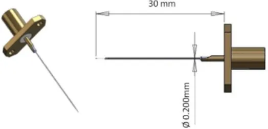
coil diameter to micrometric dimensions (200 µm - 20 µm) implies reducing the coil wire diameter, too. As a result, the amplitude of the current injected into the probe must be reduced to avoid any deterioration of the coil. Consequently, the power that can be effectively injected into such probes was experimentally found too small for disturbing significantly the behavior of the logic device. After several attempts and prototype versions, we adopted a probe shown in Figure 7. It is constituted of a thin tungsten rod. Its main characteristics are: a length of 30mm, and a diameter of 200 µm at one end and 10 µm at the other end.
Fig. 7. Unipole micro-probe
This probe involves predominantly electric field, and we can assume that only this component, at the tip end, can couple with the metal tracks inside the IC. Further information about the platform and the effects of EM injection are available in [6, 7].
3.3 Attack Description
Inside the EMC table top test enclosure, the probe was located in the close vicinity of the FPGA plastic seal (the FPGA packaging was left intact), i.e. at a distance of roughly 100 µm from the DUT packaging. In order to maximize the impact of EM injections, the tip of the probe was placed near ROs implemented inside the FPGA.
– The first set of experiments, realized on Target#1, was aimed at analyzing the influence of EM injections on the ROs. The EM signals power level Pforward was set successively to [34 nW ; 340 µW ; 1 mW ; 3 mW], in a
frequency range [300 MHz – 325 MHz]. With a sampling rate of 20 MS/s, we acquired 10 traces on each of the four oscilloscope channels, in order to record:
• Out1, the signal provided by the RO#1 used as a trigger to synchronize
the oscilloscope.
• Out2to Out4, the signals provided by RO#2, RO#3 and RO#4.
Finally, all acquired data were analyzed off line according to several criteria. Among them, one is the mutual information. This point is detailed in section 4.2. Another one (detailed in section 4.3) is the phase difference between the oscillating signals Out1 and Out3with EM injection.
next section.
4
Effect of the EM Waves on the ROs - Target #1
4.1 Choice of the injection frequency
The frequency of the injected signal determines success of the attack. Indeed, the coupling between the IC and the probe tip end depends strongly on this parameter.
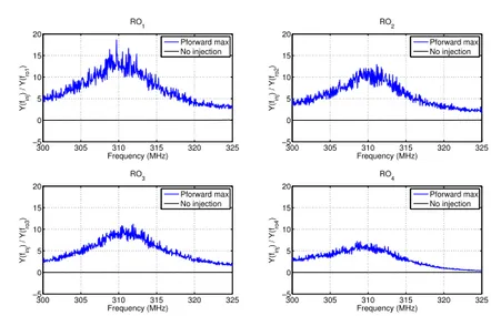
Our first aim was to find the frequency that will impact a maximum number of ROs. For this reason, the EM injections were realized at different frequencies. More precisely, the frequency was swept over the range of [300 MHz - 325 MHz] by steps of 50 kHz. This range was chosen because the oscillating frequencies fROi of all ROs were measured and found to be spread between 325 MHz and 330 MHz. During frequency sweeping, we analyzed the evolution of the following ratios: DFTRi= Yfinj/YfROi; where Yfinjis the amplitude of the spectral decomposition of Outiat the injected frequency and YfROi is the amplitude at fROi. As shown Figure 8, within this frequency range, all the DFTRi ratios reach their maximum value at around f=309.7 MHz. For this reason and also because this frequency maximizes the EM injection effects on all ROs, it was selected for realizing all the following experiments. Figure 9b illustrates the effect of the EM injection at this frequency. It can be seen that the spectral decomposition of Out1 and
Out3shows a maximum at 309.7 MHz during perturbation signal injection. This
maximum is fifteen times higher than the amplitude at fRO1 and fRO3, because ROs oscillate at the injected frequency. However, this also means that all the ROs (or at least most of them) are mutually locked.
The selected frequency was kept unchanged during the rest of experiments and also during the specific attacks on TRNGs.
When the RO was not perturbed by an EM injection, only the fundamental frequency composed the signal and its magnitude was equal to 0.25 (Figure 9a). As a result, the DFT factor was near to 0. Then, the EM harmonic signal of 309.7 MHz was injected. The 309.7 MHz harmonic was so strong that it appeared on the DFT and the amplitude of this harmonic became fifteen times higher than that of the fundamental frequency (Figure 9b). This injected harmonic signal took the control of ROs and generated signals.
300 305 310 315 320 325 −5 0 5 10 15 20 RO1 Frequency (MHz) Y(f in j ) / Y(f ro 1 ) Pforward max No injection 300 305 310 315 320 325 −5 0 5 10 15 20 RO2 Frequency (MHz) Y(f in j ) / Y(f ro 2 ) Pforward max No injection 300 305 310 315 320 325 −5 0 5 10 15 20 RO3 Frequency (MHz) Y(f in j ) / Y(f ro 3 ) Pforward max No injection 300 305 310 315 320 325 −5 0 5 10 15 20 RO4 Frequency (MHz) Y(f in j ) / Y(f ro 4 ) Pforward max No injection
Fig. 8. Discrete Fourier Transforms (DFT) factor Yfinj/YfROi vs injection frequency,
after analyzing signals Out1, Out2, Out3 and Out4.
3 3.1 3.2 3.3 3.4 x 10⁸ 0 0.1 0.2 0.3 0.4 0.5 Frequency (MHz) |Y(f)| a) No injection 3 3.1 3.2 3.3 3.4 x 10⁸ 0 0.5 1 1.5 2 2.5 3 Frequency (MHz) |Y(f)| b) PForward=3mW Out3 Out1 Out3 Out1 ∆F
Fig. 9. Discrete Fourier Transform of the signals Out1 and Out3 under: a) normal
conditions b) EM injection at Finj=309.7MHz Pf orward=3mW
4.2 Proof of Effectiveness
In order to verify that all ROs were effectively locked, we analyzed the evo-lution of the mutual information (MI) between the four ROs output voltages (Vi(t),Vj(t)) for the injected power Pforward. The MI is a general measure of the
dependence between two random variables, and this parameter is often used as a generic side-channel distinguisher [8]. Concerning our experiments, we expected to observe:
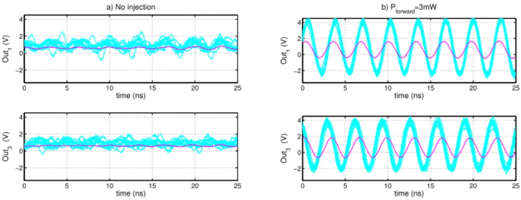
This clearly demonstrates that the ROs were locked or at least interdependent. This interdependence was also visible on the oscilloscope thanks to the persis-tence of the screen. Figure 10) shows signals Out1 and Out3 obtained without
(Figure 10a) and with (Figure 10b) signal injection. As it can be seen, if un-der attack, the two ROs were synchronized and operated at the same frequency (note, that for other ROs we observed the same behavior).
Table 1. MI values for selected RO couples obtained at different injection powers PForward 309.7 MHz 340 nW 34 µW 1 mW 3 mW MI(RO#1,RO#2) 0.0267 0.1746 0.5478 1.5729 MI(RO#1,RO#3) 0.0305 0.7697 0.7889 1.1029 MI(RO#1,RO#4) 0.0135 0.2838 0.6747 0.8221 MI(RO#2,RO#3) 0.1055 0.1086 0.3872 0.8379 MI(RO#2,RO#4) 0.0245 0.1332 0.2247 0.6477 MI(RO#3,RO#4) 0.0383 0.3196 0.8053 0.9382 MI average 0.0398 0.2983 0.5715 0.9870 0 5 10 15 20 25 −2 0 2 4 a) No injection Out 1 (V) time (ns) 0 5 10 15 20 25 −2 0 2 4 Out 3 (V) time (ns) 0 5 10 15 20 25 −2 0 2 4 b) Pforward=3mW Out 1 (V) time (ns) 0 5 10 15 20 25 −2 0 2 4 Out 3 (V) time (ns)
Fig. 10. Subsequent traces in persistent display mode (bold) and mean traces (fine) of Out1 and Out3 corresponding to RO’s outputs during a) normal conditions and b)
4.3 Phase Reduction
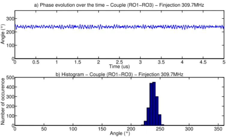
Under normal conditions, the ROs have different operating frequencies due to different interconnection delays. This is visible in Figure 9a. The difference ∆F = fRO1− fRO3 produces a linear drift between the rising edges of the ROs signals (their positions will also depend on the jitter, but compared to ∆F , the jitter impact is smaller). 0 0.5 1 1.5 2 2.5 3 3.5 4 4.5 5 0 100 200 300 Time (us) Angle (°)
a) Phase evolution over the time − Couple (RO1−RO3) − Finjection 309.7MHz
0 50 100 150 200 250 300 350 0 100 200 300 400
500 b) Histogram − Couple (RO1−RO3) − Finjection 309.7MHz
Angle (°)
Number of occurence
Fig. 11. a) Phase difference between Out1 and Out3over the time b) Phase
Distribu-tion.
In the case of strong EM harmonic injections, the two ROs are locked on the injection frequency. This is clearly visible in Figure 9b, where the biggest harmonic is the one of the injected frequency. Next, we propose to evaluate the phase difference between output signals of two ROs. The evolution of the phase differences between signals Out1 and Out3 is plotted in Figure 11a. According
to the histogram from Figure 11b, the phase is distributed between 222˚and 252˚and centered around 237˚. This gives a range of variation for the phase of 30˚. If we look at the phase evolution over the time, it is following an almost sinusoidal tendency. As said before, during the harmonic injection, Out1 and
Out3 are mainly composed of two frequencies, one coming from the injection
itself (finj) and the working frequency of the ring (fRO1 and fRO3). These two frequencies in the frequency spectrum of each RO produce a beat phenomenon (as it is defined in acoustics). This beat phenomenon explains the sinusoidal tendency of the phase.
1 Gb of data (1000 sequences of 1 Mb). It is recommended and common to evaluate a bitstream starting by the frequency test (also called monobit test), which evaluates the balance between number of ones and zeros in the bitstream. If this test does not pass, it is not reasonable to continue with other tests.
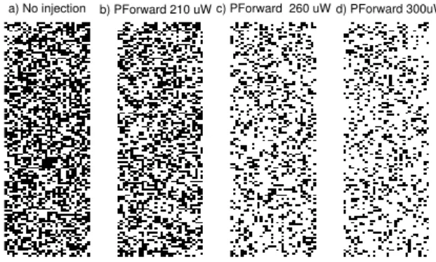
a) No injection b) PForward 210 uW c) PForward 260 uW d) PForward 300uW
Fig. 12. Bitstream produced by the TRNG under different attack powers at 309.7 MHz using electric probe (120x32) - Starting from left to right: a) No injection b) PForward = 210 µW c) PForward = 260 µW d) PForward = 300 µW
Table 2. Statistical parameters of the TRNG output bitstream PForward No Injection 210 µW 260 µW 300 µW
Bias% 0.1% 15.87% 51.57% 55% NIST tests SUCCESS FAIL FAIL FAIL
In Table 2, the bias is defined as Bias = abs(0.5 − P (0)) = abs(0.5 − P (1)), where P(x) is the probability of the element x. The bias can vary between 0 and 0.5. The bias is usually reported in %, after extrapolation between 0% and 100% corresponding to 0 and 0.5 bias values. We will use this bias representation in the rest of the paper. A good TRNG must have a bias close to 0%.
According to Figure 12 and Table 2, the EM injection effect on the bias is clear. For example, for a power of 210 µW (Figure 12b the bias reaches 15% (15 bits out of 100 bits of the bitstream are impacted by signal injection). Increasing
the injected power up to 260 µW, the bias raises up to 50% (Figure 12c and Figure 12d).
5.2 Control of the Bias
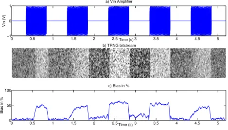
Previous experiments confirmed that it is possible to control statically the bias of a RO based TRNG. In the next experiments, we wanted to observe the dynamic behavior of the TRNG under attack. We added an amplitude modulator (AM) between the RF generator and the input of the power amplifier. This system achieves the analog multiplication between the injection signal – a sine waveform signal fixed at 309.7 MHz (the active harmonic needed to perform the attacks) – and a square waveform signal (the control signal), which controls accurately the beginning and the end of the EM injection. The control signal is provided by an external FPGA to deliver a desired timing injection sequence. Figure 13a represents the timing evolution of the AM signal in Volts. Figure 13b shows the effect on the TRNG output bitstream. Finally, Figure 13c represents the evolution of the bias in time. It was computed using a sliding window of 10 000 bits. The sliding step was 32 bits.
0 0.5 1 1.5 2 2.5 3 3.5 4 4.5 5 −1 0 1 Time (s) Vin (V) a) Vin Amplifier b) TRNG bitstream 0 0.5 1 1.5 2 2.5 3 3.5 4 4.5 5 0 50 100 Time (s) Bias in % c) Bias in %
Fig. 13. a) AM signal - b) TRNG stream of bits (raster scanning from bottom to top and left to right) - c) Bias in % for the TRNG stream of bits.
Looking at the bitstream or the bias, it is clear that the behavior of the TRNG is quickly (in less than 1 ms) impacted by the EM perturbation and it returns to its initial state with the same speed. In fact, we observed that the bias was changing according to the dynamics of the power amplification chain. In our case, it has a time response of roughly 1 ms. The difference in the bias
TRNG bitstream 0 1000 2000 3000 4000 5000 6000 7000 8000 0 10 20 30 0 50 100 150 200 250 300 350 400 450 500 0 50 100 Bias in % Time(s) Bias in % 0 50 100 150 200 250 300 350 400 450 500 −1 0 1 Vin Amplifier Time (s) Vin (V)
Fig. 14. a) AM signal b) There might be something written in this stream of bits -c) Bias in % for the TRNG stream of bits.
In order to demonstrate different capabilities of the proposed EM attack, a complex square waveform signal was generated by an external FPGA in order to replace the 1 Hz signal previously used to modulate the injected frequency; the carrier wave frequency was kept at 309.7 MHz. In order to implement such an experiment and to maintain the same amplifier in the injection chain, we had to decrease the sampling frequency of the TRNG from 24 KHz to 500 Hz. This sampling frequency modification had an impact on the output bitrate of the TRNG, but not on its capability to produce a good quality random bitstream, which passes the tests. The control sequence was arranged in such a way, that we obtained the bitstream from Figure 14. As shown, the word COSADE appears in the stream of bits. This definitely demonstrates that the EM harmonic injection constitutes an important threat for RO based TRNG.
6
Conclusion
In this paper, an active EM attack on RO-based TRNG is presented. The ex-periment setup is first described, and details about the EM harmonic platform and the DUTs are provided. The first study of the behavior of the source of entropy in the TRNG, i.e. of the set of ROs, showed the efficiency of the EM emanations in controlling the behavior of ROs by their locking on the injected signal, depending on the power of the injected signal and its frequency. In a sec-ond experiment, realized on a 50-RO Wold’s TRNG implemented in an FPGA, we demonstrated that it was possible dynamically control the bias of the TRNG output.
7
Acknowledgments
The work presented in this paper was realized in the frame of the EMAISeCi project number ANR-10-SEGI-005 supported by the French ”Agence Nationale de la Recherche” (ANR).
References
1. A. T. Markettos and S. W. Moore, ”The Frequency Injection Attack on Ring-Oscillator-Based True Random Number Generators”, Cryptographic Hardware and Embedded Systems (CHES2009), 2009, pp. 317-331.
2. K. Wold and C. H. Tan, ”Analysis and Enhancement of Random Number Generator in FPGA Based on Oscillator Rings”, International Conference on Reconfigurable Computing and FPGAs (ReConFig’08), 2008, pp. 385-390.
3. B. Sunar, W.J. Martin, and D.R. Stinson, ”A Provably Secure True Random Num-ber Generator with Built-In Tolerance to Active Attacks”, IEEE Transactions On Computers, 2007, vol. 56, no. 1, pp. 109-119.
4. AIST, Side-channel Attack Standard Evaluation Board (SASEBO) http://staff.aist.go.jp/akashi.satoh/SASEBO/en/index.html.
5. T. Dubois, S. Jarrix, A. Penarier, P. Nouvel, D. Gasquet, L. Chusseau and B.Azais, ” Near-field electromagnetic characterization and perturbation of logic circuits”, Proc. 3rd Intern. Conf. on Near-Field Characterization and Imaging (ICONIC’07), 2007, pp. 308-313.
6. F. Poucheret, K. Tobich, M. Lisart, B. Robisson, L. Chusseau and P. Maurine, ”Local and Direct EM Injection of Power into CMOS Integrated Circuits”, Fault Diagnosis and Tolerance in Cryptography (FDTC 2011).
7. F. Poucheret, B. Robisson, L. Chusseau and P. Maurine, ”Local ElectroMagnetic Coupling with CMOS Integrated Circuits”, International Workshop on Electromag-netic Compatibility of Integrated Circuits (EMC COMPO 2011).
8. L. Batina, B. Gierlichs, E. Prouff, M. Rivain ,F.X. Standaert and N. Veyrat-Charvillon, ”Mutual Information Analysis: A Comprehensive Study”, Journal of Cryptology pp. 1-23 (2010).