HAL Id: emse-00530148
https://hal-emse.ccsd.cnrs.fr/emse-00530148
Submitted on 1 Aug 2013HAL is a multi-disciplinary open access archive for the deposit and dissemination of sci-entific research documents, whether they are pub-lished or not. The documents may come from teaching and research institutions in France or abroad, or from public or private research centers.
L’archive ouverte pluridisciplinaire HAL, est destinée au dépôt et à la diffusion de documents scientifiques de niveau recherche, publiés ou non, émanant des établissements d’enseignement et de recherche français ou étrangers, des laboratoires publics ou privés.
Wire-bonding on inkjet-printed silver pads reinforced by
electroless plating for chip on flexible board packages
Romain Cauchois, Mohamed Saadaoui, Jacques Legeleux, Thierry Malia,
Béatrice Dubois-Bonvalot, Karim Inal, Jean-Christophe Fidalgo
To cite this version:
Romain Cauchois, Mohamed Saadaoui, Jacques Legeleux, Thierry Malia, Béatrice Dubois-Bonvalot, et al.. Wire-bonding on inkjet-printed silver pads reinforced by electroless plating for chip on flexible board packages. ESTC 2010. Electronics System Integration Technology Conference, Sep 2010, Berlin, Germany. pp.AP-4, �10.1109/ESTC.2010.5642997�. �emse-00530148�
Wire-Bonding on Inkjet-Printed Silver Pads Reinforced by Electroless Plating
for Chip on Flexible Board Packages
Romain Cauchois1,2, Mohamed Saadaoui2, Jacques Legeleux2, Thierry Malia1, Béatrice Dubois-Bonvalot1 Karim Inal2, Jean-Christophe Fidalgo1
1
Gemalto – Innovation and Manufacturing Technologies Department, Avenue du Pic de Bertagne 13881 Gemenos - France
2
Ecole Nationale Supérieure des Mines de Saint-Etienne, Microelectronics Center of Provence (CMP) 880, avenue de Mimet 13541 Gardanne - France
[email protected] - +33 442 616 745
Abstract
The nanoporous nature of the inkjet printed silver nanoparticles entail low hardness and surface effective contact area for being compatible with pads that are suitable for wire-bonding in electronic packaging. Electroless nickel plating is a selective metal deposition technique which can brings the required thickness and hardness for further pads processing. Here, a 1.7 µm thick nickel layer is deposited on top of 600 nm thick printed and sintered silver nanoparticles using Kapton polyimide as substrate. Prior to plating, a special attention was put on tuning microstructures of printed silver pads by sintering nanoparticles at various temperature ramps (0.1, 10 and 50°C/s) up to 200°C. Results show that fast sintering exhibits the lowest electrical resistivity which is suitable in printed interconnects. However, wire-bonding on nickel pads is best achieved when low sintering ramp is used. This slow sintering presents the highest adhesion strength at the nickel/silver interface since the pores dimensions were restricted to the nanoscale. The validation of the optimized bonding process came from the low electrical contact resistance between plated nickel and the bonded gold wire, and from the wire-pull test which is in accordance with the MIL-STD 883 standard. The actual results show that a compromise has to be found when emphasis is on patterning low resistive interconnects or stiff pads for wire-bonding applications. This compromise is tailored by the sintering engineering.
Introduction
Metallic nanoparticles have been widely studied over the past few years notably for their applications in microelectronics [1-3]. In addition to its use as a filler in conductive (ACA/ACF) and non-conductive (NCF) films dedicated to fine-pitch flip-chip applications [4], nanoparticles can be used to perform circuitry on rigid or flexible substrates after being dispersed in a solvent based vehicle [5]. Prevalence of their high surface area to volume ratio and its benefit on sintering activation by reducing melting temperature has been reported in previous works [6, 7]. Those colloidal suspensions exhibit a high processability which enables the use of high resolution and low cost techniques especially inkjet printing. This technique allows the reduction of process steps by a factor of three compared with common photolithography. The later is basically divided in six steps consisting in coating the base layer with several materials, before masking to transfer the circuitry patterns from a dedicated mask. After that, etching and stripping steps are performed. On comparison, inkjet is limited to
the pattern direct printing on the base layer and to the curing of the deposited ink in order to remove solvents, to initiate the film cohesion and to improve electrical contact between nanoparticles. This curing step can be carried out using either a conventional oven or other selective techniques such as laser, microwave and joule heating [8-10]. This additive approach is thus time and cost-saving for the fabrication of 2D interconnects and passive electronics. Nonetheless, films produced by this technique are usually nanoporous which simultaneously affects the electrical and the mechanical properties of printed structures [11].
In this paper, we report on new developments of wire-bondable pads for flexible chip-on-board and lead-frame applications using thin films made of sintered silver nanoparticles followed by nickel electroless plating. In fact, low electrical resistivity of nanoporous silver is obtained through the optimization of sintering temperature ramps. Mechanical characterization shows that the Young’s modulus and hardness still has to be improved for gold wire bonding process. This is achieved by surface finishing using nickel plating that shows a dependence to the initial microstructure of printed silver pads especially by affecting adhesion strength at the silver/nickel interface. The present technology is demonstrated through the implementation of IC chips in flexible boards.
Tuning of inkjet printing parameters
Patterns have been designed and printed using 40 nm silver nanoparticles ink on A4 Kapton sheet. Test structures include Kelvins, wire-bonding chain pads, a lead-frame for IC chips rerouting and squares for Young’s modulus measurements and pull-off adhesion characterization. An in-line inkjet printer prototype developed in the lab (JetPac) was employed to pattern the test vehicle. This fully automated prototype allows sequential pre-treatment and post-processing of printed substrate. The inkjet system is based on drop-on-demand technique which operates by propelling 30 pL droplets through each of the 256 nozzles. Ejections are driven by a bipolar pulse waveform sent to a piezoelectric print head which control the volume and the ejection velocity of droplets. An automaton ensures the coordination between the conveyor speed and the piezoelectric operating frequency for achieving patterns with line width inferior to 100 µm. A commercially available 125 µm thick Kapton HN polyimide substrate from DuPont has been selected for its flexibility, chemical resistance and low shrinkage behaviour at curing temperature up to 350°C.
Figure 1: Inkjet-printed test structures on Kapton
substrate.
Inkjet process parameters, such as meniscus and droplets ejection velocity, have been finely tuned to achieve high resolution patterns and defect free interconnects. Time of flight adjustment also ensures the quality of the pattern by preventing formation of satellite drops and by reducing geometrical discrepancies.
Microstructural evolution with sintering
Once silver lines are properly printed on the substrate, their electrical conduction is activated by the evaporation of solvents and by the sintering of metallic nanoparticles. Both of these steps are activated by thermal energy. The sintering step is achieved by providing thermal energy to nanoparticles in order to initiate diffusion regimes that will consequently cast bonds between nanoparticles. This phenomenon, called the Gibbs-Thomson effect, results from significant contributions of the surface energy to the free energy of the system. Due to their high value of surface area to volume ratio, diffusion regimes in silver nanoparticles are activated at lower temperature than the bulk melting point (961°C) [12, 13]. Nonetheless, densifying and non-densifying sintering regimes have been previously identified as consuming the given thermal energy. Control of the time-temperature couple showed that these various regimes diverge as much by their physical mechanisms [14, 15] as by their effects on pore density reduction and thin-film shrinkage.
The electrical properties of the printed thin-film are closely linked to the time and temperature couple during sintering. Since the mean free path of electrons in silver (=53nm) is of the same order of the nanoparticles average radius (<r0>=40nm), electrical resistance between
nanoparticles is a combination of ohmic and ballistic transport. This physical phenomenon has been modelled by Wexler function (see equ. 1) which states that the higher the contact area between nanoparticles is, the lower the electrical resistivity will be [16]:
2
3
4
)
(
a
a
K
R
W
(1)where K, (K), a are respectively the Knudsen number (), a factor of the order of unity, the bulk resistivity and the contact radius. Sintering of nanoparticles is thus a critical step toward, promoting grain growth and controlling pores density. By optimizing thermal annealing, different electrical and mechanical properties can be achieved.
Previous work included the optimisation of thermal sintering process conditions for performing low-resistive
interconnects on silicon nitride substrate [17]. The use of organic substrates indeed greatly limits the sintering temperature because of the low glass transition temperature and the high coefficient of thermal expansion. For this purpose, the working temperature on Kapton is then fixed at 200°C.
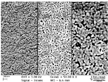
When sintering temperature is fixed, microstructure of printed features can be tailored with the thermal ramping. Annealing experiments have been performed in nitrogen atmosphere using a Rapid Thermal Anneal (RTA) oven between room temperature and 200°C, at 0.1°C/s, 10°C/s and 50°C/s. Microstructural response to these sintering conditions is shown in Figure 2 through SEM observations.
Figure 2: Surface microstructures of silver interconnect
after sintering at 0.1, 10 and 50°C/s (resp. from left to right) via SEM observations.
According to Figure 2, increasing the heating rate tends to enhance both the grain growth and the Ostwald ripening of porosities. Image analysis was performed to derive microstructural parameters such as the number of porosities by unit of area (density), the average Feret’s diameter of porosities which relates with their size distribution (see table below).
Table 1: Microstructural properties derived from image
analysis.
0.1°C/s 10°C/s 50°C/s
Porosities density (µm-²) 139 78 36 Avg. Feret’s diameter (nm) 47 65 88
The mean grain diameter is growing from 24 nm to 57 nm, according the ramp. This grain growth of silver nanoparticles is intended to reduce interconnects electrical resistivity, regarding Equation 1. However, grain growth comes along with a merge of porosities which limits the film densification and can worsen its conductivity (see Table 2).
Microstructural evolution of printed films was linked to their electrical performances through the measurement of Kelvin test structures. Results are reported jointly with the mean grain size in Table 2.
Table 2: Microstructural and electrical evolution of
printed silver nanoparticles under different thermal ramping (200°C, 15min)
0.1°C/s 10°C/s 50°C/s
Resistivity (µOhm-cm) 5.01 4.52 3.77 Mean grain diameter
(nm) 24 42 57 Structures treated at 0.1°C/s show no densification compared with the initial state. Indeed, the mean grain size is similar to the initial nanoparticles size, as if microstructure has been frozen throughout the solvent evaporation step in spite of sintering bonds development. Advanced sintered state is attested by a resistivity of 3.8 µOhm-cm. Interconnects having undergone a 10 and 50°C/s ramp clearly exhibit grain growth and porosities merging which affect electrical conduction as seen in Table 2. The poor densification and high pore size is attributed to the low temperature treatment and to the increasing thermal shock caused on polyimide substrate during RTA treatment. Despite good electrical performances, the aim of the present work is more focused on optimizing the microstructures of printed silver nanoparticles for further wire-bonding experiments.
Interconnects reinforcement by electroless nickel plating
Nanoporous films usually exhibit different mechanical properties compared to the bulk, especially when the elastic modulus and hardness are considered [18]. Basically, those two parameters have low values that are greatly affected by the porosity as well as by the grain size. For successful wire-bonding operation, a thick and harder pad metallization is required in order to absorb the stress resulting from wire loading.
The direct bondability of gold wire on printed silver pads has been performed by connecting the lead-frame to the IC chip. It has been observed that whatever the microstructure of silver, the bonding step failed. Pad damages including silver splash and lifting are observed (see Figure 3) showing that both cohesive and adhesive fracture modes occurred. Those failure observations were attributed to the low Young’s modulus and hardness of sintered silver pads, compared to the gold mechanical properties.
This key issue has been addressed using selective electroless nickel plating for pads reinforcement for gold wire bonding. This process has been widely adopted in microelectronics industry for the past few years as a consequence to lead-free solders specifications and for under-pads damage protection. Electroless nickel is an auto-catalytic process that is deposited from a hypophosphated nickel bath.
Ni2+ + H2PO2- + H2O Ni + H2PO3- + 2H+
Figure 3: SEM image of the gold ball bonding failure on
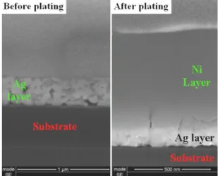
a printed silver pad, showing layer decohesion and lift. For electroless nickel plating on porous printed silver pads, a high pH nickel bath is used at 65°C since acidic plating bath tends to chemically etch the silver pads. The growth of electroless nickel has been performed during 5 min in order to achieve a 1.7 µm-thick nickel layer. This thickness is sufficient to improve the wear mechanical resistance and the film hardness and tends to clog the film porosities (See Figure 4 and Figure 5).
Figure 4: Surface microstructures of electroless nickel
plating, showing characteristic nickel nodules, on silver sintered at 0.1, 10 and 50°C/s (resp. from left to right) via SEM observations.
Figure 5: SEM view of tilted cross-section of the pad
Young’s modulus of inkjet-printed silver nanoparticles has been determined by nanoindentation system in continuous stiffness measurement mode at 45 Hz using Berkovich tip. In order to take into account the high disparity of porosities on silver surface, 64 indentations has been performed on each sample and the resulting average is presented in Figure 6.
Figure 6: Load vs. displacement curves of inkjet-printed
silver film before and after electroless nickel process. The Bec model has been used to extract the film Young’s modulus from the reduced one corresponding to the film/substrate composite measured by the equipment [19]: s C f C C C i i r A E A E t A t A E E 2 2 ) 1 ( 2 1 1 2 2 (2)
where E and are the Young’s modulus and Poisson’s ratio (r, i, f and s subscripts stand respectively for reduced, indenter, film and substrate properties), Ac is the
projected contact area and t is the film thickness.
Figure 7: Variation of Young's modulus (histogram) and
of initial pore densities (curve) according the thermal treatment before and after electroless nickel plating process.
Extracted Young’s moduli are consistent with microstructures observed before. Indeed, the Young’s Modulus is greatly influenced by the presence of pores in the printed structures. In the case of high porosities size, the modulus shrinks to half the bulk Young’s modulus. On the other hand, nickel plating increases the overall modulus to values higher than 100 GPa in all cases, due to anisotropic nickel growth. Results from Figure 7 show that the Young’s modulus is all the more great that the porosity content is high. Nonetheless, in all cases, Ni-Au plating enabled wedge-bonding of 25µm diameter gold wire with a bonding force comprised between 18 and 20g (see Figure 8).
Figure 8: Gold wire-bonds on silver printed structures
plated with electroless nickel process on a polyimide substrate.
Packaging performance
Once the feasibility is demonstrated, the process has to be validated by proving its capability in microelectronics systems. A lead-frame has thus been purposely designed and inkjet-printed on a polyimide substrate to host an IC chip in order to test performance of package from adhesion of plated interconnects to wire-bonds robustness, including contact resistance measurements between plated pads and gold wire. The testing package is shown on Figure 9.
Figure 9: Dummy flexible package with wire-bonds from
an IC chip to plated lead frame (front right and bottom) and between plated pads (front left).
Thermosonic bonding process involves ultrasonic waves together with thermal heating of the wire. The pads thus have to be stiff enough and sufficiently bounded to the substrate to resist such treatment. Pull-off test consists in sticking pre-treated aluminium studs on both side of the film/substrate system [20]. The microporous surface of the studs enables mechanical interlocking of the adhesive after crosslinking. Both studs are then separated applying a normal load until break is observed. Experiments were conducted on silver films with and without electroless nickel plating to illustrate the influence of the process on the adhesion quality (see Figure 10). Experimental results indicate a marked degradation of adhesion properties of the film to the substrate after the plating step. It is believed that the acidic solutions used during electroless nickel plating are the cause of this degradation since cyanide ions in solution corrode silver atoms and thus weaken physicochemical bonds between film and substrate.
Figure 10: Results of pull-off test performed on printed
silver films (black square) and electroless nickel plated films (red circle).
Robustness of wire bonds is evaluated performing wire-pull tests along the vertical axis. Due to the central position of the hook on the loop, this test sollicitates the wedge bonds both in normal and shear load. During the tests, 90% of the failure modes involved neck break of the wedge bond located at the die side. The maximum pull load remains constant at 3.6g whatever the previous thermal treatment. This shows the good surface finishing of the electroless nickel plating on silver which enables repeatability of the bonding process in an industrial environment without changing bonding parameters.
The good adhesion of gold wires to reinforced pads ensures sufficient electrical conduction for signal transmission while the device is under operation. Nonetheless, the interface between gold and nickel presents a given contact resistance that has to be measured to prove applicability of the whole process. A chain of wire bonds has been processed on Kelvin type structures printed and consequently plated with Ni/Au. Four point probing was used to eliminate the contact resistance of the probe tip during measurements. While current is injected and collected at both ends of the chain, each connection is probed in order to be averaged.
Contact resistance measurements show no tendency with variations comprised between 10mOhm and 45 mOhm.
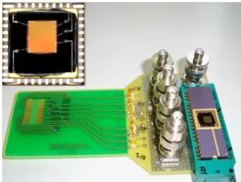
Figure 11: Apparatus used for functionality tests where
the chip-on-flex has been reported in a ceramic package (inset view) to be plugged-in an ISO test board.
The final validation came from the functionality test of the assembly where the IC-chip interconnected to the printed lead-frame using the above-mentioned technology has been reported in a ceramic package. The reporting step has been performed to be compatible with conventional electrical testing for microelectronic devices. Smartcard ISO pads on a PCB permitted Answer to Request query of the device, a test which happened to be conclusive with full functionality. This final test validated the pertinence of using inkjet printing jointly with electroless plating finishing for packaging applications.
Conclusions
In this paper, we reported the latest developments on inkjet-printed interconnects compatibility with standard wired connections. Wedge bonding of 25 μm diameter gold wire has been performed on finished surfaces using electroless nickel immersion gold plating process. Electrical and microstructural characterization of the base silver layer has been performed so that the latching of the nickel growth could be tailored. The challenge, here, was to successfully perform wired connections on printed and malleable bond-pads whose thickness can fall down to 300 nm. The improved mechanical behaviour measured by nanoindentation has been correlated to the good performances of the wedge bonding, both electrically and mechanically in tensile stress. Robustness of the wired connections seemed controlled more by the surface state of nickel layer than to the initial microstructure of silver layer. A functionality test finished to validate the process exposed in this paper for chip-on-flexible devices.
The prospective advantage of direct printing for interconnects and bond-pads technologies combined with electroless plating is thus a good alternative to conventional metallization techniques and offers new opportunities for low cost and flexible electronic packages.
Acknowledgments
Presented printings were conducted on the JetPac equipment, an inkjet printer prototype developed in the lab with funding from EU (ERDF) and local authorities’ research initiatives. This work was supported by the EURIPIDES office through COSY-3D project.
References
1. Lu, G. Q. et al, “Low-temperature and pressureless sintering technology for performance and high-temperature interconnection of semiconductor devices”, Proc International conference on thermal,
mechanical and multi-physics simulation experiments in microelectronics and micro-systems, Apr. 2007, pp.
609-613.
2. Yamaguchi, T. et al, “Sintering mechanism of composite nanoparticle and its application to bonding in electronics”, Proc Materials Science and
Technology Conference, 2006.
3. Moon, K. S. et al, “Thermal behavior of silver nanoparticles for low-temperature interconnect applications”, Journal of Electronic Materials, Vol. 34, No. 2 (2005), pp. 168-175.
4. Li, Y. Et al., “Novel Monolayer-enhanced Non-Conductive Film (NCF) for Ultra-Fine Pitch High Performance Interconnect in Lead-free Electronics”,
Proc Electronic Components and Technology Conference, 2007, pp. 1911-1915.
5. Kim, D. et al, “Direct writing of silver conductive patterns: Improvement of film morphology and conductance by controlling solvent compositions”, Applied Physics Letters, Vol. 89, No. 26 (2006), pp. 264101–3.
6. Buffat, P. and Borel, J. P., “Size effect on the melting temperature of gold particles”, Physical Review A, Vol. 13, No. 6 (1976), pp. 2287-2298.
7. Safaei, A. et al, “Modelling the size effect on the melting temperature of nanoparticles, nanowires and nanofilms”, Journal of Physics: Condensed Matter, Vol. 19, No. 21 (2007), pp. 216216.
8. Ko, S. H. et al, "All-inkjet-printed flexible electronics fabrication on a polymer substrate by low-temperature high-resolution selective laser sintering of metal nanoparticles", Nanotechnology, Vol. 18 (2007), pp. 345202-345209.
9. Perelaer, J. et al, "Ink-jet Printing and Microwave Sintering of Conductive Silver", Advanced Materials, Vol. 18 (2006), pp. 2101-2104.
10. Allen, M. L. et al, “Electrical sintering of nanoparticle structures”, Nanotechnology, Vol. 19, No. 17 (2008), p. 175201.
11. Xiang, Y. et al, “Mechanical properties of porous and fully dense low-k dielectric thin films measured by means of nanoindentation and the plane-strain bulge test technique”, Journal of Material Research., Vol. 21, No. 2 (2006), pp. 386-395.
12. Buffat, P. and Borel, J.-P., “Size effect on the melting temperature of gold particles”, Physical Review A, Vol. 13, No. 2 (1976), pp. 2287-2298.
13. Allen, G. et al, “Small particle melting of pure metals”, Thin Solid Films, Vol. 144, No. 2 (1986), pp. 297-308.
14. German, R. M., Sintering Theory and Practice, Wiley-Interscience (1996).
15. Swinkels F. B. and Ashby M. F., “A second report on sintering diagrams”, Acta Metallurgica, Vol. 29, No. 2 (1981), pp. 259-281.
16. Wexler G., “The size effect and the non-local Boltzmann transport equation in orifice and disk geometry”, Proc. Phys. Soc., Vol. 89, No. 4 (1966), pp. 927-941.
17. Cauchois, R. et al, “Thermal optimization of silver nanoparticles sintering for low resistive printed applications”, Proc 20th MicroMechanics Europe Workshop, Toulouse FR, Sept. 2009, pp.368-371.
18. Greer, J. R. and Street, R. A., “Mechanical characterization of solution-derived nanoparticle silver ink thin films”, Journal of Applied Physics, Vol. 101, No. 10 (2007), pp. 103529-35.
19. Bec, S. et al, “A simple guide to determine elastic properties of films on substrate from nanoindentation experiments”, Philosophical Magazine, Vol. 86, No. 33-35 (2006) , pp. 5347-5358.
20. Turunen, M. P. K. et al, “Pull-off test in the assessment of adhesion at printed wiring board metallisation/epoxy interface”, Microelectronics Reliability, Vol. 44 (2004), pp. 993-1007.