HAL Id: hal-01908196
https://hal.archives-ouvertes.fr/hal-01908196
Submitted on 23 Nov 2018
HAL is a multi-disciplinary open access
archive for the deposit and dissemination of
sci-entific research documents, whether they are
pub-lished or not. The documents may come from
teaching and research institutions in France or
abroad, or from public or private research centers.
L’archive ouverte pluridisciplinaire HAL, est
destinée au dépôt et à la diffusion de documents
scientifiques de niveau recherche, publiés ou non,
émanant des établissements d’enseignement et de
recherche français ou étrangers, des laboratoires
publics ou privés.
substitution on the optoelectronic and excitonic
properties of layered hybrid perovskites
Joshua Leveillee, Claudine Katan, Liujiang Zhou, Aditya Mohite, Jacky Even,
Sergei Tretiak, André Schleife, Amanda Neukirch
To cite this version:
Joshua Leveillee, Claudine Katan, Liujiang Zhou, Aditya Mohite, Jacky Even, et al.. Influence of π
-conjugated cations and halogen substitution on the optoelectronic and excitonic properties of layered
hybrid perovskites. Physical Review Materials, American Physical Society, 2018, 2 (10), pp.105406.
�10.1103/PhysRevMaterials.2.105406�. �hal-01908196�
Influence of
π
-conjugated cations and halogen substitution on the optoelectronic and excitonic
1
properties of layered hybrid perovskites
2
Joshua Leveillee,1, 2,∗Claudine Katan,3Liujiang Zhou,2 Aditya Mohite,4
3
Jacky Even,5Sergei Tretiak,2Andr´e Schleife,1, 6, 7 and Amanda J. Neukirch2, †
4
1Department of Materials Science and Engineering, University of Illinois at Urbana-Champaign, Urbana, IL 61801, USA
5
2Los Alamos National Laboratory, Los Alamos, NM 87545, USA
6
3Univ Rennes, ENSCR, INSA Rennes, CNRS, ISCR - UMR 6226, F-35000 Rennes, France
7
4Department of Chemical and Bimolecular Engineering, Rice University, Houston, TX 77006, USA
8
5Univ Rennes, INSA Rennes, CNRS, Institut FOTON - UMR 6082, F-35000 Rennes, France
9
6Frederick Seitz Materials Research Laboratory, University of Illinois at Urbana-Champaign, Urbana, IL 61801, USA
10
7National Center for Supercomputing Applications, University of Illinois at Urbana-Champaign, Urbana, IL 61801, USA
11
(Dated: November 8, 2018)
12
Low-cost chemical engineering of two-dimensional layered hybrid halide perovskite structures allows for the design of hybrid semiconductor quantum wells with tailored room temperature excitonic optical absorption, emission, and charge carriers transport properties. Here density functional theory and the Bethe-Salpeter equa-tion are used to predict the electronic structure and optical response of layered perovskites with two represen-tative single-ring conjugated organic spacers, ammonium-propyl-imidazole (API) and 2-phenethylammonium (PEA). The inorganic perovskite quantum well properties are further tuned by analyzing the effect of halogen (X=I, Br, Cl) substitution. We found that visible light absorption occurs primarily within the perovskite layer and that UV light absorption induces partial electron-hole separation between layers. In addition, a strong exciton binding energy and influence on absorption spectrum is found by solving the Bethe-Salpeter equation. Our re-sults suggest that further engineering is necessary beyond the single-ring limit, by introducing more conjugated rings and/or heavier nuclei into the organic spacer. This is a promising future direction to achieve photo-induced charge separation and more generally hybrid heterostructures with attractive optoelectronic properties.
I. INTRODUCTION
13
Three-dimensional (3D) hybrid organic-inorganic
per-14
ovskites (HOPs) have rapidly emerged as some of the most
15
promising thin-film photovoltaic materials.1–3 Their allure
16
comes from a combination of high photo-conversion
ef-17
ficiency (PCE), low device processing cost due to
low-18
temperature solution processing, and composition from
earth-19
abundant and readily available materials. In particular,
hy-20
brid lead-halide perovskite (e.g. methylammonium lead
io-21
dide, MAPbI3, and formamidinium lead iodine, FAPbI3) solar
22
cells have undergone a PCE increase from 3.5 % to over 20 %
23
in about 5 years.4–6 These devices have currently exceeded
24
the certified record efficiency of multicrystalline Si cells.7
25
Beyond photovoltaic applications, HOPs show potential in
26
many other fields including hydrogen generation,8X-ray and
27
Gamma-ray detection,9–12 light emitting diodes (LEDs),13
28
spintronics,14,15and sensors.16Setting aside the issue of lead
29
toxicity,17–22the main impediment to industry deployment of
30
perovskite devices is their instability to air, moisture,23 and
31
light exposure.24,25
32
Recently, layered HOPs (LHOPs) have re-emerged as
33
promising alternatives to their 3D counterparts. They
34
have been suggested to be used as highly efficient white
35
LEDs26 and tunable optical detectors.27 In these, quantum
36
confinement effects within perovskite layers can be
engi-37
neered and tailored to specific applications.28–31 In
particu-38
lar, they are able to overcome some of the above-mentioned
39
limitations,32–34 by offering much improved stability and
40
decent photo-conversion performance: Tsai et al. reported
41
that non-encapsulated single crystals of
n-butylammonium-42
methylammonium lead-iodine with n=3 and 4 layers resists
43
moisture-driven chemical degradation. They also showed that
44
encapsulation of the crystals resulted in no chemical
degrada-45
tion under highly illuminated conditions, and built solar cells
46
with a PCE of 12.5 with n=3 and n=4 layers %.32The broad
47
applications and variability of LHOPs have opened a field of
48
research that is just beginning to produce deeply insightful and
49
practically applicable results.
50
The LHOPs studied in this work fall into the
Ruddlesden-51
Popper crystal class35 and their characteristic structure
con-52
sists of 2D layers of n corner-sharing metal-halide octahedra
53
separated by, and ionically bonded to, large charged
poly-54
atomic cations (see Fig. 1). The inorganic perovskite layer
55
can be tuned to a specific width of n octahedra or even cleaved
56
along various planes, linking the octahedra in linear or zig-zag
57
corrugated patterns.36–38 Opportunities to engineer LHOPs
58
not only originate from changing the inorganic perovskite
59
stoichiometry, but also by choosing one or more of many
60
complex large organic cations to separate the layers.26,36–39
61
Promising organic cations range from simple carbon chains
62
with ammonium caps to large chromophore complexes.40–42
63
These degrees of freedom allow for the exploration of a wide
64
variety of electronic properties and to tune optical response.
65
In this context, optically activated charge separation
be-66
tween the organic and inorganic layers of LHOPs has been
67
long sought to reduce the overlap between electron and
68
hole wave functions and, thus, allow utilization of separated
69
electron-hole channels for highly efficient charge transport.
70
The advent of organic solar cells has proven thatπ-conjugated
71
polymers are fully capable of producing and transporting
72
bound electron-hole pairs (excitons) under illumination.43,44
73
It has further been suggested that inter-chain charge
sep-74
aration of bound electron-hole pairs is possible in these
75
(a) (b) (c) (d)
FIG. 1. (Color online.) The atomic structure of ammonium-propyl-imidizole (API)-PbBr4projected along the (a) [100] direction and (b) [010] direction and 2-phenethylammonium (PEA2)-PbBr4projected along the (c) [100] and (d) [010] axis. The stacking direction is [001]. Atomic color coding: Pb (red), Br (blue), C (black), N (green), and H (pink). Tilting angleδ and bond angle η are indicated (see text).
systems.45 Furthermore, charge transfer between
semicon-76
ductor CdSe quantum dots and
poly[2-methoxy-5-(2-ethyl-77
hexyloxy-p-phenylenevinylene)] bonded functional coatings
78
has been observed.46 This raises an interesting question
79
whether organic layers in LHOPs withπ-conjugated organic
80
cations could similarly carry photo-current under illumination
81
if optical absorption excites electrons and holes that are
lo-82
calized in parallel layers of the LHOP system. If so,
exten-83
sive chemical degrees of freedom in LHOPs could allow for
84
engineering a layered organic-inorganic compound material
85
that are capable of efficiently separating electrons and holes.
86
These layers may provide separate conduction channels for
87
electrons and holes, potentially reducing detrimental
recombi-88
nation. However, it is unknown how active theπ-conjugated
89
organic compounds in LHOPs are under UV-VIS absorption,
90
in particular in the stoichiometric limit of n=1 perovskite
lay-91
ers between each organic layer.
92
To address this, Li et al. conclude from a large Stokes
93
shift in the photoluminescence emission spectrum that charge
94
separation occurs between the organic
ammonium-propyl-95
imidazole (API) layer and inorganic PbBr4perovskite layer
96
of [110] oriented API lead-bromide (n=1).47 They also
per-97
formed density functional theory (DFT) calculations and
re-98
port an isolated carbon-π∗ state in the fundamental band
99
gap, to which they attribute the carrier separation and
re-100
sulting massive Stokes shift. However, this material has not
101
been studied by modern first-principles approaches that
in-102
clude the effects of spin-orbit coupling (SOC) and
electron-103
hole interaction on the optical-absorption spectrum. In
par-104
ticular, SOC has shown to be very important in
determin-105
ing the correct electronic band structure in Pb-containing
hy-106
brid perovskite materials.14,15,29,48Furthermore, several
rea-107
sons for a large Stokes shift are debated and no conclusion
108
has been reached: It has been suggested recently that it
orig-109
inates from strongly bound small-polaron states that form in
110
the perovskite layer, lowering the emission energy of
electron-111
hole pairs.49,50 While the extent of octahedral tilting in and
112
out of the perovskite plane has also been correlated with the
113
magnitude of the Stokes shift,51,52 Du et al. found no such
114
correlation from their analysis of the optical absorption and
115
emission character of layered Pb(I,Br,Cl)4 perovskites with
116
acene alkylamine organic cation layers.53Hence, the debate
117
to what extentπ-conjugated organic layers participate in the
118
optical absorption and emission of LHOPs is still open.
119
In the present study, we report first-principles calculations,
120
for singleπ-conjugated LHOPs to determine the organic and
121
inorganic layer contributions to electronic structure and
op-122
tical absorption. We also clarify at what energies this
be-123
comes a significant contributor to the total optical response.
124
The materials of interest are the⟨110⟩ API-PbX4class (X=I,
125
Br, Cl) of layered perovskites, motivated by the work of Li et
126
al.47and the singleπ-conjugated organic cation perovskites
2-127
phenyl-ethylammonium (PEA) PEA2-PbX4(X=I, Br, Cl) due
128
to their readily available experimental atomic geometries and
129
singleπ-conjugated (benzene) group per organic ion (see Fig.
130
1). We compute the ion-projected electronic structure and
131
single-particle optical response using density functional
the-132
ory (DFT), including spin-orbit coupling (SOC) and band gap
133
corrections determined by HSE06 hybrid-functional
calcula-134
tions. The PBE+SOC+∆HSE06 calculations reported in this
135
work are an approximation of the full single-particle
exci-136
tation energy calculations within the GW +SOC many-body
137
perturbation theory formalism.54The two-particle optical
re-138
sponse, which includes the effect of exciton formation, is
139
calculated from the solution of the Bethe-Salpeter equation
140
(BSE). Our results clarify energetic alignment of the bands
141
associated with organic and perovskite components in both
142
materials and provide detailed analysis of essential electronic
143
wavefunctions and individual contributions to optical
absorp-144
tion spectra. This allows us to answer the question whether
145
optical excitations occur within individual layers of single
146
π-conjugated LHOPs or whether optical excitations partially
147
separate electrons and holes between layers.
148
(a) (b) (c)
(d) (e) (f)
FIG. 2. (Color online.) The ion-projected band structures, computed using PBE+SOC+∆HSE06, of API-PbBr4(a-c) and PEA2-PbBr4(d-f). The color bar indicates the contribution of Pb (red), Br (blue), and API/PEA (magenta) to each state as a percentage.
RESULTS
149
Atomic Structure: The structure of single-layer ⟨110⟩
150
API-PbX4 compounds resembles that of the ⟨100⟩ class of
151
layered perovskites: The major difference is the corrugation
152
of the perovskite layer with a zig-zag type octahedral linking
153
in the⟨110⟩ compounds and a linear-type linking in the ⟨100⟩
154
compounds. Figure 1 shows the [100] and [010] projections of
155
both API-PbBr4and PEA2-PbBr4. PEA2-PbX4experimental
156
structures are used in our study.55–57Since experimental data
157
is available only for API-PbBr4,47we fully relax all API-PbX4
158
atomic geometries in the P21/c symmetry space group. The
159
resulting lattice parameters and vector angles, unit-cell
vol-160
umes, octahedron tilting angles, and Pb–X–Pb bond length
161
ranges are reported in supplemental information (SI) Table
162
S1 for all systems. The relaxed API-PbBr4atomic structure
163
is in excellent agreement with the experimental structure
de-164
termined by Li et al.,47 with errors of under 1 % for lattice
165
parameters, 0.2 % for unit-cell volume, 1 % for lattice vector
166
angles, 2.5 % for out-of-plane tilting, and 15 % for in-plane
167
tilting angles. The out-of-plane tilting anglesδ1andδ2in the
168
corrugated⟨110⟩ API-PbX4systems should be 45◦, if no
tilt-169
ing is present. For the relaxed API-PbX4structures we find
170
two distinctδ1andδ2in the range between 33.7◦and 33.8◦
171
and 51.4◦and 53.9◦, respectively.
172
In the linearly-linked PEA2-PbX4systems,δ=0◦under no
173
tilting and indeed in the experimental structures, the
out-of-174
plane tilting angles remain small, in the range of 1◦ to 3◦.
175
The in-plane-tilting angles, ranging between η=12.2◦ and
176
η=14.5◦, are larger compared to those found in the API-PbX4
177
systems, ranging fromη=8.5◦toη=10.5◦. This in-plane
tilt-178
ing is very similar to the octahedron tilting in orthorhombic
179
MAPbX33D HOPs.58
180
Electronic Structure: The band structures of API-PbX4
181
and PEA-2PbX4 reveal dispersive band frontiers attributed
182
to states localized on the perovskite as well as flat,
non-183
dispersive bands, situated more than 1 eV away from the band
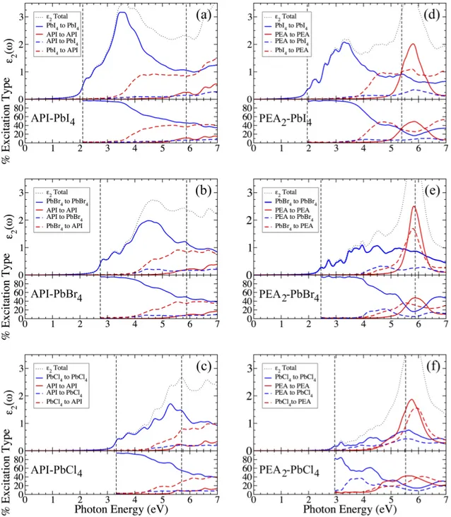
184
frontiers, that are attributed to the organic π andπ∗ states
185
(see Fig. 2). Throughout the remainder of the paper, the
la-186
bel PBE+SOC+∆HSE06 refers to the PBE+SOC band
struc-187
ture with conduction bands rigidly shifted to higher energy to
188
match the HSE06+SOC band gap, and HSE06+SOC refers to
189
fully non-collinear HSE06 hybrid-functional calculations that
190
take SOC into account. Table I reports relevant calculated and
191
experimentally determined energy gaps of these materials.
192
Ion-projected PBE+SOC+∆HSE06band structures are
plot-193
TABLE I. Energy gaps (in eV) computed using different levels of theory. PBE+SOC+∆HSE06refers to the PBE+SOC electronic struc-ture with the band gap rigidly shifted to the HSE06+SOC band gap value (see text).
Level of theory API-PbI4 API-PbBr4 API-PbCl4 PBE+SOC 1.44 1.94 2.41 HSE06+SOC 2.10 2.74 3.32 π – π∗gap (PBE+SOC+∆HSE06) 5.87 5.88 5.7
BSE Optical gap 1.74 2.23 2.68 Exp. Optical gap47 – 3.18 –
PEA2-PbI4 PEA2-PbBr4 PEA2-PbCl4 PBE+SOC 1.33 1.75 2.12 HSE06+SOC 1.95 2.45 2.95 π – π∗gap (PBE+SOC+∆HSE06) 5.39 5.82 5.53
Exp. optical gap53 2.45 3.0 3.6
ted for API-PbBr4in Fig. 2(a)-(c). Similar data for the other
194
API and PEA LHOPs considered in this work can be found
195
in SI Figs. S2 and S3. Due to the P21/c symmetry, the
API-196
PbX4materials exhibit direct gaps of 2.10 eV, 2.74 eV, and
197
3.32 eV for API-Pb(I, Br, and Cl), respectively, at the Y point
198
of the Brillouin zone (BZ). The Y point folds back to the Γ
199
point when a 2×2 conventional cell is considered as
demon-200
strated by Pedesseau et al.29The band gap we computed for
201
API-PbBr4 using the HSE06 exchange-correlation functional
202
with spin-orbit coupling underestimates the gap of 3.18 eV
203
measured from the optical onset by Li et al..47 This can be
204
attributed to the fact that HSE06, albeit it improves over the
205
DFT-PBE description, does not fully capture quasiparticle
ef-206
fects for the systems studied here. More sophisticated, but
207
computationally more expensive methods, such as many-body
208
perturbation theory, could mitigate these shortcomings.59
Ad-209
ditionally, in this comparison the electron-hole interaction was
210
neglected and, thus, the calculated electronic gap differs from
211
the measured optical gap by the exciton binding energy. This
212
will be discussed in the results for optical response.
Dif-213
ferences between our relaxed structure and the experimental
214
structure of API-PbBr4 are expected to result in only small
215
changes of the band gap, within 0.2 eV, based on the
ef-216
fects of in- and out-of-plane angles on gap values explored by
217
Pedesseau et al..29 Figure 2 clearly shows that the band
dis-218
persion of API-PbBr4along the Y –Γ direction is free-electron
219
like, with a parabolic curvature near the Y point. Along the
220
Y – A direction, the dispersion has a lower curvature,
indicat-221
ing a higher electron effective mass. Finally, along the Y – C
222
direction the bands are effectively flat due to the layered and
223
reduced periodicity of the LHOP crystals along the [001]
di-224
rection. We observe the same trend for API-PbI4 and
API-225
PbCl4.
226
In contrast, band structures of the PEA2-PbX4LHOPs, with
227
space groups P21/c, P¯1, and P¯1 for I, Br, and Cl, respectively,
228
exhibit direct gaps of 1.95 eV, 2.45 eV, and 2.95 eV at the
Γ-229
point. The difference between the space groups of PEA2-PbI4
230
and PEA2-Pb(Br,Cl)4is due to the bis-phenylethylammonium
231
conformation of the chosen PEA2-PbI4structure.53The
gen-232
eral PEA2 conformation explored by Du et al. assumed the
233
same P¯1 space group as the PEA2-PbBr4 and PEA2-PbCl4
234
systems. The band structure of PEA2-PbBr4, illustrated in
235
Fig. 2(d)-(f), exhibits highly dispersive, free-electron like
236
band frontiers along theΓ – X and Γ –Y directions, as well
237
as flat, non-dispersive band frontiers in the Γ – Z direction.
238
Unlike the API-PbX4corrugated perovskites, the PEA2-PbX4
239
perovskites explored in this work are not corrugated in
ei-240
ther in-plane direction. Thus, they have a higher
periodic-241
ity in both in-plane lattice directions which manifests itself in
242
highly dispersive band frontiers along two reciprocal-lattice
243
directions. As a consequence, corrugated API-PbX4 shows
244
low effective-mass band frontiers only alongΓ –Y, whereas
245
PEA2-PbX4shows low effective masses along bothΓ – X and
246
Γ –Y.
247
In traditional 3D HOPs such as MAPbX3, valence and
con-248
duction band frontiers are comprised of X:p+Pb:6s and Pb:6p
249
states, respectively.60 While in principle, in the layered
sys-250
tems with conjugated organic cations explored in this work,
251
API and PEAπ andπ∗ states could contribute in the
near-252
gap region, we find from the ion-projected band structure that
253
the valence and conduction band frontiers are comprised of
254
X:p+Pb:6s and Pb:6p states, respectively. This is very
simi-255
lar to the 3D MAPbX3HOPs. However, unlike 3D MAPbX3
256
HOPs that have organic states far below (about 6 eV) and
257
above the band frontiers,60API-PbX4and PEA2-PbX4have
258
flat, non-dispersive bands attributed to API and PEA2π and
259
π∗orbitals within 1.0 to 2.0 eV of the band frontiers, as shown
260
in Fig. 2.
261
Furthermore, due to the strong contributions of Pb-derived
262
states to the band frontiers in API-PbX4and PEA2-PbX4, the
263
spin-orbit interaction lowers the energy of conduction-band
264
minimum states (see Fig. S5). This energy reduction of
265
Pb:p conduction-band states is well known in Pb- and
Sn-266
containing HOP and LHOP systems14,15,29,48 and attributed
267
to the large mass of Pb atoms. Hence, SOC-related energy
268
contributions are critical for correctly predicting the energetic
269
ordering of states near the band-extrema and, in particular, to
270
qualitatively explain the relative energy position of organic
271
π andπ∗states. In Fig. 2 (as well as Figs. S4 (a) and (b)
272
and S5 (a) in the SI) we clearly show that once SOC is taken
273
into account, the ion-resolved band ordering at theΓ-point
274
conduction band minimum changes: The Pb:p states are
low-275
ered in energy relative to the API π∗ states which remain
276
unaffected by the spin-orbit interaction. As a result, we
ob-277
serve Pb:p character for all k points throughout the BZ. In
278
contrast, without the inclusion of SOC, a band inversion
oc-279
curs at theΓ-point and the conduction band minimum would
280
be attributed to mostly APIπ∗ states. Hence, if SOC is
ne-281
glected, electronic-structure calculations could, depending on
282
transition matrix element amplitude, incorrectly predict that
283
excitations from theΓ-point band frontiers result in charge
284
separation between perovskite and API layers. This
behav-285
ior is different from what has been observed for 3D MAPbX3
286
HOPs, for which ion projection of the band frontiers remain
287
the same, with X+Pb and Pb attributed to the valence and
con-288
duction band frontiers, respectively,60 whether or not SOC
289
is included. Finally, we note that the difference between
290
HSE06+SOC and the PBE+SOC+∆HSE06 approach is
mini-291
mal, and PBE+SOC+∆HSE06calculations are a good basis for
292
optical response calculations. To this end we show in detail
293
in the SI that for optical excitations energies below 5 eV, only
294
small errors of under 0.5 eV are expected for spectral features.
295
FIG. 3. (Color online.) The PBE+SOC+∆HSE06ion-projected DOS of (a) API-PbI4, API-PbBr4, API-PbCl4and (b) PbI4, PEA2-PbBr4, and PEA2-PbCl4. The energies of the Pb 5d states at−15.3 eV are used for alignment, and the valence band maxima of API-PbI4 and PEA2-PbI4are used as energy zero. Dashed lines mark the band extrema. Color coding: Pb (red), halide (blue), organic layer (shaded brown).
The ion-resolved density of states (DOS) in Fig. 3
illus-296
trates that in all six perovskite systems, the valence- and
297
conduction-band frontiers are attributed to halide and Pb
298
states, respectively. For this analysis, we aligned the Pb:5d
299
states at−15.3 eV across the different materials. Importantly,
300
Fig. 3 shows a reduction of the valence-band maximum in
en-301
ergy with decreasing halide mass: The valence band maxima
302
of API-PbX4shift from 0.0, to −0.24, and −0.48 eV for X
303
= I, Br, and Cl, respectively. The same trend of the valence
304
band maximum located at 0.0,−0.17, and −0.47 eV occurs
305
for the PEA2-PbX4 systems for X = I, Br, and Cl,
respec-306
tively. This decrease can be understood by examining
stan-307
dard atomic ionization energies of halide atoms, with I, Br,
308
and Cl having ionization energies of 10.45, 11.81, and 12.96
309
eV (from the NIST Atomic Spectra Database Ionization
Ener-310
gies Form).61Since the valence-band maximum of each
per-311
ovskite material in this work is attributed to halide p-states,
312
our findings are commensurate with trends of these atomic
313
ionization energies.
314
At the same time, this figure shows that organicπ andπ∗
315
states are not affected by the changing halide mass and remain
316
approximately aligned in both systems. The APIπ states
ap-317
pear as broad peaks at−2.00, −1.78, and −1.40 eV for I, Br,
318
and Cl, respectively. This broadening is due to static
molec-319
ular disorder and coupling between organic molecular states.
320
The lowest energyπ∗states appears as sharp peaks centered
321
around 3.87, 4.10, and 4.30 eV for I, Br, and Cl, respectively.
322
The resultingπ–π∗gaps, defined as the energy differences
323
of these peaks, are 5.87, 5.88, and 5.70 eV and show a width
324
of about 0.5 eV from the broadening of theπ∗ state. The
325
PEA2-PbX4systems display a highest occupiedπ state peak
326
spanning the range between−1.3 and −2.1 eV. A single
low-327
est unoccupiedπ∗peak is located between 3.84 and 4.10 eV
328
for all PEA2-PbX4 materials. This leads to π–π∗ gaps of
329
5.39, 5.82, and 5.53 eV for I, Br, and Cl, respectively, with a
330
width of about 1.0 eV. The variations in theπ–π∗gaps in the
331
PEA2-PbX4systems are attributed to differences in the
exper-332
imental X-ray atomic structures of the organic layers used in
333
the unit cells of this study. As we chose to relax the
API-334
PbX4 structures (due to the similarities of the relaxed and
335
experimental API-PbBr4structures and the lack of available
336
experimental data for API-Pb(I,Cl)4) theπ–π∗gaps are
uni-337
form across the choice of halide. We note that quasiparticle
338
corrections computed within HSE06+SOC also produce an
339
energy-dependent band dilation, not reproduced by the scissor
340
approach. This increases theπ–π∗gaps of the API and PEA
341
systems to about 6.1 – 6.3 eV, suggesting thatπ–π∗optical
342
transitions will occur well in the UV photon energy range.
343
The PBE+SOC+∆HSE06 approximation captures the UV
re-344
sponse of the intra-organic transitions, albeit at slightly lower
345
energies compared to HSE06+SOC, and therefore provides a
346
reasonable approximation for optical response calculations. It
347
should be mentioned that, in reality, the absorption onset of
348
such molecules is at lower energies due to large exchange
en-349
ergy contributions. For example, benzene in an alcohol
solu-350
tion has an absorption onset of about 4.8 eV.62However, this
351
is still in the UV energy range.
352
Figure 3 also shows that, due to a lower cation charge of
353
+1 on PEA compared to +2 in API, the ratio of organic to
354
inorganic density of states is higher in the PEA2-PbX4
struc-355
tures. This implies that, if organic-perovskite optical
transi-356
tions are allowed, the PEA2-PbX4systems have more possible
357
charge-separation pathways under optical excitation. In
ex-358
amining the ion-resolved density of states of API-PbX4, it can
359
be seen that the optical response below the 5.7 eVπ–π∗gap
360
contains mostly transitions between perovskite-derived states.
361
Only small contributions due to transitions from
perovskite-362
to API-derived states are expected between the optical onset
363
and 5.7 eV. This changes in the PEA2-PbX4systems, where
364
the PEA density of states amplitude in the valence and is about
365
equal to or greater than the perovskite density of states at the
366
PEAπ-state energy. Consequently, the optical response could
367
have a large contribution from perovskite to PEA transitions
368
at lower energies than the π–π∗ gap. This implies that if
369
transitions between perovskite and PEA are optically allowed,
370
the PEA2-PbX4systems have more possible charge separation
371
states available.
372
Finally, in the context of achieving charge separation
be-373
tween organic and perovskite layers upon optical excitation,
374
we find that PEA2-PbCl4is a particularly promising
candi-375
date. The ion-resolved DOS in Fig. 3 shows a pronounced
376
peak associated with the organic molecule that is centered
377
near 1.5 eV below the valence-band maximum. Not only is
378
this peak higher in energy than another peak at−2 eV that is
379
attributed to Cl ions, but it also is of the same magnitude, as
380
discussed above. This energetic positioning of states suggests
381
the strong potential for partial charge separation, generating
382
holes in the PEA2πstate and electrons in the conduction-band
383
Pb:6p state. The actual probability of charge separation
be-384
tween layers, however, depends again on the dipole matrix
el-385
ements for the corresponding optical transitions between these
386
organic and perovskite states. This will be discussed next.
387
Optical Response: The ion-projected dielectric function
388
ε2(ω) is illustrated in Fig. 4 for all considered materials.
389
Here we distinguish between transitions among perovskite
390
ions (’inorganic’) and organic cations (’organic’) by bundling
391
them into the ininorganic, organic,
organic-392
inorganic and inorganic-organic subcategories. The first two
393
correspond to intra-layer transitions and the latter two to
inter-394
layer transitions. If the two sub-layers were to act as separate
395
optically active materials, the amplitude of inter-layerε2(ω)
396
is vanishing. In the case of intra-layer optical excitation, these
397
projections are finite.
398
By ion-resolving the imaginary dielectric function of
API-399
PbX4, we show that optical excitations below 4 eV are entirely
400
dominated by intra-perovskite transitions, whereas inter-layer
401
transitions contribute significantly to the optical response
402
above 4 eV. As discussed above, this is because states in the
403
vicinity of the gap are attributed entirely to perovskite states
404
(Fig. 3). Absorption between API-derived states, with an
on-405
set around theπ–π∗gap, contributes weakly to the overall
406
optical response even in the UV energy range due to a low
407
relative API-π density of states compared the halide density
408
of states in the valence band. Figure 4 also shows that
transi-409
tions from PbX4to API states are responsible for a significant
410
portion of the optical response in the UV energy range, and
411
thus partial electron and hole separation occurs between the
412
API and PbX4 layers. However, this partial separation has
413
little utility for optoelectronic applications requiring charge
414
separation for visible light energy excitations.
415
The PEA2-PbX4 systems demonstrate a much stronger
416
intra-organic optical response within the PEA layers, along
417
with significant inter-layer absorption in the UV energy range.
418
As with API-PbX4, the near-gap and visible energy range of
419
the spectra is governed by intra-perovskite optical response.
420
Around theπ–π∗gap, a large peak appears in the imaginary
421
dielectric function which is attributed to the intra-PEA optical
422
transitions and transitions from PbX4to PEA states.
Transi-423
tions from PbX4 to PEA states appear at higher energies at
424
lower halide masses, corresponding to the increased VBM-π∗
425
gap by the decrease in the valence band energy. In PEA2
-426
PbI4, strong transitions are observed from PbI4to PEA states
427
at lower energies than those between PEA states, leading to
428
the same partial charge separating activity seen in API-PbX4
429
above 4 eV. In PEA4-PbBr4, the contributions due to
transi-430
tions from PbBr4to PEA and PEA to PbBr4are roughly equal
431
in the 4 to 5 eV photon range, leading to a cancellation in
par-432
tial charge separation character due to hybridization. PEA2
-433
PbCl4shows a change in behavior: The optical response
be-434
tween 3.5 and 4 eV largely arises from intra-perovskite
tran-435
sitions and contributions from PEA to PbCl4states, partially
436
separating holes to the PEA layer and electrons to the PbCl4
437
layer. This behavior is due to the proximity of the PEA π
438
states to the PbCl4attributed valence band maximum, leading
439
to inter-layer transitions closer to the absorption onset.
How-440
ever, overall, in PEA2-PbX4, where the organic optical
activ-441
ity is more significant compared to API-PbX4, partial charge
442
separation only occurs in the UV energy range.
443
In all three LHOP API-PbX4 compounds, excitonic
ef-444
fects are expected to be stronger compared to their 3D HOP
445
MAPbX3counterparts owing to quantum and dielectric
con-446
finement effects.30 This increased binding energy was first
447
explained by the works of Rytova and Keldysh, who
sep-448
arately established the theory of quantum confinement of
449
charge carriers and the Coulomb interaction in low
dimen-450
sional systems.63,64This was further explored in layered
semi-451
conductors by Hanamura and layered perovskites by Ishihara
452
and Koutselas.65–68In 3D HOPs such as MAPbI3, MAPbBr3,
453
and MAPbCl3, the high-frequency dielectric constantsε∞are
454
about 4 – 7.48,69–71MAPbX
4also has highly dispersive band
455
frontiers, leading to a low reduced electron-hole mass of about
456
0.1m0.72 Using a simple Wannier-Mott model, the exciton
457
binding energy is in the range of 25 to 85 meV. As determined
458
in experiments and predicted by theory, the low-frequency
di-459
electric constants are also large (εs > 20), which enhances
460
the screening of the electron-hole Coulomb potential.29,72–75
461
Given the API-PbBr4electronic structure determined in this
462
work, the high-frequency dielectric constant is determined to
463
be 3.94 by density-functional perturbation theory (DFPT) and
464
the reduced electron-hole mass at the band frontiers is
ap-465
proximately 0.610m0, based on an averaged parabolic fit to
466
the dispersive, in-plane, Y → G and Y → A directions. This
467
leads to a Wannier-Mott binding energy of 525 meV, which
468
is an order of magnitude higher compared to the 3D
counter-469
parts. The lower high-frequency dielectric constants predicted
470
by DFPT range from 3.47 to 4.76 for the LHOP systems (see
471
Tab. S2) and originate from the alternating low and high
val-472
ues ofε∞between layers averaged over the unit cell volume.76
473
This leads to an average dielectric constant that is lower than
474
those typically measured and calculated for 3D HOPs.29,30
475
The excitation energies of lone API molecules in air are
476
calculated in the Gaussian suite77 to determine if the organic
477
optical response will comprise a significant portion of the
478
optical response near the perovskite absorption edge. The
479
HSE, B3LYP, and CAM-B3LYP functionals are used to
cal-480
culate the homo-lumo gaps of 5.60, 5.84, and 8.05 eV
respec-481
FIG. 4. (Color online.) The ion-resolved imaginary dielectric functions of (a) API-PbI4, (b) API-PbBr4, (c) API-PbCl4, (d) PEA2-PbI4, (e) PEA2-PbBr4, and (f) PEA2-PbCl4. The color coding indicates the resolution ofε2along specific ion-to-ion transitions, which are (in valence ions→ conduction ions notation) perovskite→perovskite (blue, solid), organic→organic (red, solid), organic→perovskite (blue, dashed), perovskite→organic (red, dashed), and all (black, dotted). The bottom panels show the percent that each type of transitions contributes to the totalε2as a function of photon energy.
tively in the singlet-relaxed geometry. The HSE and B3LYP
482
agree very well with theπ-π∗ gap found in API-PbX4at the
483
PBE+SOC+∆HSE06 level of theory. Excitation energies are
484
calculated using time-dependent DFT and are found to be
485
5.42, 5.23, and 5.75 eV within the HSE, B3LYP, and
CAM-486
B3LYP functionals, respectively. These results suggest that
487
the excitonic absorption onset of the API spacer will not
oc-488
cur near the perovskite excitonic absorption edge.
489
Strong excitonic effects and, hence, large exciton
bind-490
ing energies are predicted for the API-PbX4 materials from
491
first principles, with values comparable to available
experi-492
mental data for LHOP systems. For API-PbX4, we show in
493
Fig. 5 that excitonic effects significantly influence the
optical-494
absorption spectra. The gradual absorption onset observed in
495
FIG. 5. (Color online.) Imaginary part of the dielectric function of API-PbI4(top), API-PbBr4(middle), and API-PbCl4(bottom) with (red lines) and without (black lines) excitonic effects. The PBE+SOC Kohn-Sham energies and states are used as input to the BSE and the single-particle band gap is shifted to the HSE06+SOC value. That band gap and the lowest excitation from the BSE are marked by ver-tical black and red dashed lines, respectively.
the single-particle dielectric function becomes a pronounced
496
excitonic peak, red-shifted to lower energy, that is
associ-497
ated with the lowest-energy electron-hole bound state. In
498
addition, there is also a significant red shift of broad
high-499
energy peak structures between 3.5 eV and 4.5 eV, resulting in
500
strongly increased absorption at lower energies. In our
calcu-501
lations, the energy difference of the onsets of single-particle
502
and BSE spectrum correspond to the binding energy of the
503
lowest electron-hole pair. The high computational cost of the
504
BSE calculations in this work, due to large unit cells and
in-505
clusion of spin-orbit coupling, does not allow a dense enough
506
multiple k-point sampling78to provide fully converged results
507
for this quantity. Given the choice of k-point mesh, we
esti-508
mate that our numbers are within 100 meV of the converged
509
result (see SI figure S6). From our data we extract≈357 meV
510
(see Fig. 5) for the exciton-binding energy of API-PbI4, which
511
is the smallest value for the three API-PbX4compounds
stud-512
ied in this work. API-PbBr4shows a stronger exciton binding
513
energy due to the lower dielectric constant compared to
API-514
PbI4, and consequently a stronger red shift of the onset by
515
≈505 meV. Finally, the strongest excitonic red shift in the
op-516
tical spectrum of≈638 meV is predicted for API-PbCl4, with
517
the lowest high-frequency dielectric constant. High-frequency
518
dielectric constants are slightly overestimated as they are
cal-519
culated at the PBE+SOC level of theory. However, from
520
test calculations we estimate that increasing the band gap to
521
the experimental value would decrease the dielectric constant
522
by less than 15%. Since we do not have accurate band gap
523
data to compare with for the API-PbX4materials, we use the
524
PBE+SOC high-frequency dielectric constant as a good
ap-525
proximation.
526
The predicted exciton binding energies and relative
po-527
sitions of spectral peaks are in good agreement with
avail-528
able experimental data of layered perovskite systems.47Wang
529
et al. measured exciton binding energies of 218 meV in
530
hexadecammonium-lead bromide (HA)2PbBr4,79 Blancon et
531
al. measured binding energies of 380, 270, and 220 meV in
532
n = 1, n = 2, and n > 2-layered (BA)2(MA)n1PbnI3n+1,39and
533
Ishihara et al. calculated a binding energy of 320 meV in n=1
534
layered PbI4octahedra with no organic spacer.66As a model
535
function relying on a single, material-averaged, dielectric
con-536
stant is used to compute the screened Coulomb interaction
be-537
tween electrons and holes, we do not account for the local
538
field effects arising from the high spatial variability of the
di-539
electric constant in LHOPs.29,30More precise techniques such
540
as including the full inverse dielectric tensor εG,G′(q)−1 or
541
semi-classical and semi-empirical methods that describe
di-542
electric constant fluctuations can be used for a higher degree
543
of accuracy.29,80–82 These high binding energies are also
po-544
tentially detrimental to solar cell applications. which rely on
545
splitting of electron-hole pairs. Investigations by Smith et
546
al. have shown that the introduction of halogens by I2
inter-547
calation into the organic layer strongly reduces binding
en-548
ergy and the dielectric confinement of the layered perovskite
549
systems,83potentially lowering the exciton binding energy of
550
LHOPs which is preferable for photo-voltaic application.
551
II. CONCLUSIONS AND FUTURE DIRECTION
552
This computational study predicts that the optical
re-553
sponse of layered lead-halide perovskites with
single-554
π-conjugated organic layers API and PEA2is dominated by
555
intra-perovskite optical excitations in the visible energy range.
556
A partial charge separation between the organic perovskite
557
states can only be achieved at UV energies. Given these
re-558
sults, we conclude that single-layered PbX4LHOP systems
559
withπ-organic cation spacing layers composed of moieties
560
with single aromatic rings act as one optically active
per-561
ovskite material. Transitions involving both layers only
oc-562
cur at UV photon energies. Importantly, the lack of π and
563
π∗states near the band extrema causes transitions in the
vis-564
ible energy range to be contained within the perovskite layer,
565
meaning all electron-hole generation for optoelectronic
appli-566
cations in this energy range will be localized to the PbX4
oc-567
tahedral layers. At UV energies, significant electronic
delo-568
calization and charge separation is allowed, however the
cor-569
responding excitation energies are close to or above the
ion-570
ization energy of perovskite systems.
571
The natural follow-up question is: How can charge
separa-572
tion be further achieved in layered hybrid perovskite systems?
573
The first item that must be addressed is theπ–π∗ gap of the
574
conjugated groups. As discussed above, the absorption onset
575
of single aromatic ring moieties occurs well below the
homo-576
lumo gap due to large exciton binding energies on the order
577
of electron volts.84Benzene, with an optical onset of 4.8 eV
578
experimentally and between 4.7 and 6.9 eV theoretically by
579
PBE0+BSE and GW+BSE calculations,62,85has a predicted
580
homo-lumo gap in solution of between 4.5 and 6 eV.86
Like-581
wise, imidazole has a range of predicted excitation energies
582
between 5.61 and 6.96 eV.85Thus, the interplay between the
583
homo-lumo gap and the optical gap should be carefully
con-584
sidered in further engineering of layered perovskites for
inter-585
layer charge separation application. Ideally, the homo-lumo
586
gap can be lowered by adding more conjugated groups such
587
as aromatic rings to the system. For example, layered
per-588
ovskites with naphthalene groups have been investigated
ex-589
perimentally and have shown signs of exciton energy
trans-590
fer between perovskite and organic layers.41,42Secondly, the
591
orbital overlap between the layers must be improved to
in-592
crease the amplitude of the inter-layer transition dipole
ma-593
trix elements. Larger overlap could be achieved by
includ-594
ing heavier elements, such as chlorine, in the organic layer
595
which has been recently explored experimentally.36,38,87Our
596
future studies of such compounds will include organic-PbX4
597
ion-projected band structures and densities of states to map
598
the effects of decreased homo-lumo organic gap and organic
599
halogenation.
600
Currently, n = 1 LHOPs with single conjugated rings face
601
challenges as effective solar cell materials but show promise
602
in a wide range of optoelectronic application. Quantum
con-603
finement of the perovskite layer increases the gap relative to
604
the 3D HOPs and thus reduces the absorption range of the
ma-605
terial in the visible optical spectrum. LHOPs with n > 1 help
606
to decrease the gap,32but at the cost of reducing the density of
607
states of, and degree of optical coupling to, the organic lattice.
608
Secondly, minimalπ-stacking is observed in these systems,
609
leading to highly localized electron and hole states in the
or-610
ganic layer. This in turn results in a high effective mass, low
611
mobility in the form of incoherent hopping, and large
bind-612
ing energies of electron-hole pairs. Improvingπ-stacking of
613
the organic conjugated layer in LHOPs is a promising future
614
research direction, to achieve improvements.88Recent
inves-615
tigations have also shown that interfacing 2D LHOPs with
616
3D HOPs can lead to increased photovoltaic efficiency in
Sn-617
based systems, opening the intriguing question of whether this
618
can be done with Pb-based systems as well.89Besides
appli-619
cations as solar cells, n = 1 layered perovskites have shown
620
promise as light emitters.90 Resonant coupling between the
621
organic and perovskite layered of n = 1 systems opens the
622
possibility of engineering the emission wavelength and
inten-623
sity as a function of LHOP stoichiometry.42,91
624
It is important to note that everything studied in this
625
manuscript is related purely to absorption in the singlet spin
626
state. Thus, nothing is said about relaxation in the excited
627
state or emission in the explored LHOP systems. Both triplet
628
and singlet energy levels and their post-optical absorption
dy-629
namics are fundamental to understanding how organic
com-630
pounds behave in the excited state. The interplay between
631
perovskite band energies and the organic singlet and triplet
632
states must be understood to determine excited state charge
633
transport, ion dynamics, and recombination in LHOPs with
634
conjugated organic layers. The combination of methods in
635
this work for determining optical absorption properties and
636
methods such as time-dependent density functional theory and
637
molecular dynamics can be used to predict and disentangle
638
the full optical excitation and relaxation process of conjugated
639
LHOP materials.
640
ACKNOWLEDGMENTS
641
The work at Los Alamos National Laboratory (LANL) was
642
supported by the LANL LDRD program (A.J.N., A.D.M, J.L.
643
and S.T.). The work at UIUC work was supported by the
Na-644
tional Science Foundation under Grant No. CBET-1437230.
645
A.D.M. acknowledges the DOE-EERE 0001647-1544 grant
646
for this work. This work was done in part at Center for
647
Nonlinear Studies (CNLS) and the Center for Integrated
Nan-648
otechnologies CINT), a U.S. Department of Energy and
Of-649
fice of Basic Energy Sciences user facility, at LANL. This
650
research used resources provided by the LANL Institutional
651
Computing Program. Calculations were additionally
sup-652
ported by the Campus Cluster program at UIUC and this
re-653
search is part of the Blue Waters sustained-petascale
com-654
puting project, which is supported by the National Science
655
Foundation (awards OCI-0725070 and ACI-1238993) and the
656
state of Illinois. Blue Waters is a joint effort of the
Univer-657
sity of Illinois at Urbana-Champaign and its National Center
658
for Supercomputing Applications. LANL is operated by Los
659
Alamos National Security, LLC, for the National Nuclear
Se-660
curity Administration of the U.S. Department of Energy under
661
contract DE-AC52-06NA25396. J.E. acknowledges financial
662
support from the Institut Universitaire de France.
663
COMPUTATIONAL DETAILS
664
DFT calculations, using the projector-augmented wave method, are
665
performed with the Vienna Ab-Initio Simulation Package (VASP).92–95 666
The generalized-gradient approximation of Perdew, Burke, and Ernzerhof
667
(PBE)96is used to describe exchange and correlation (XC). Kohn-Sham wave 668
functions are expanded into a plane-wave basis with an energy cutoff of 500
669
eV and the Brillouin zone (BZ) is sampled using aΓ-centered 4 × 4 × 2
k-670
point mesh. With this setup, total energies of the API-PbX4 structures are 671
converged to within 5 meV per formula unit. Equilibrium positions of all
672
atoms, cell volumes, and unit cell parameters are optimized by minimizing the
673
external pressure and Hellman-Feynman forces to below a threshold of 10−2
674
eV/ ˚A using the PBEsol XC functional97and an increased plane-wave cutoff
675
of 900 eV. The use of PBEsol is based on previous studies where lattice
pa-676
rameters of hybrid perovskite materials are predicted to high accuracy.58The 677
symmetries of the experimentally determined unit cell are preserved in the
678
first-principles atomic position and cell geometry relaxation. Band structures,
679
ion-resolved densities of states (DOS), and ion-resolved optical-absorption
680
spectra are calculated, taking spin-orbit coupling (SOC) into account.98The 681
high-frequency dielectric constantε∞is calculated using density functional
682
perturbation theory on a 5× 5 × 2 Γ-centered k-point mesh for API-PbX4 683
(see supplemental material Fig. S1). Band gaps are determined using the
684
Heyd-Scuseria-Ernzerhof (HSE06) hybrid XC functional99with a fraction of
685
α=0.25 exact exchange. Due to the high computational cost of including
686
SOC in hybrid functional calculations, these are performed using a 2× 2 × 2
687
Γ-centered k-point mesh.
688
Linear optical response, described by the components of the complex
689
frequency-dependent dielectric tensorε2αβ(ω), whereαandβare Cartesian
690
coordinates, is computed using the Ehrenreich-Cohen formula:76,100
691 ε2αβ(ω) = 8π2e2 Ω
∑
cvk ⟨ϕck| ˆpα|ϕvk⟩⟨ϕvk| ˆpβ|ϕck⟩∗ (εck−εvk)2 δ (εck−εvk− ¯hω) (1)PhysRevMaterials.2.105406
Here,εckandεvkare the conduction and valence band energies of the single-692
particle states at electronic wave vector k, along with their respective
Kohn-693
Sham wave functionsϕckandϕvk. ˆpβis the Cartesian component of the
mo-694
mentum operator andΩ is the volume of the unit cell. We use PBE+SOC
695
Kohn-Sham energies and wave functions and a scissor shift to adjust the
en-696
ergies of the conduction bands to the HSE06+SOC band gap (referred to as
697
PBE+SOC+∆HSE06). The transition-matrix elements in Eq. (1) are computed 698
using the VASP code.76 699
We also compute the ion- and angular-momentum resolved optical
re-700
sponse by weighting the transition-matrix element for a given transition using
701
the projection pN
lmnkof the wave functionϕnkon a spherical harmonic Ylmfor 702
a given ion N, with m and l being the magnetic and orbital quantum number,
703
respectively.101The sum of pN
lmnkover all N, l, and m equals to one for each 704
wave functionϕnk. This turns Eq. (1) into: 705 ε2αβ(ω) = 8π2e2 Ω
∑
cvk (∑
N,l,m pNlmnk ) ⟨ϕck| ˆpα|ϕvk⟩⟨ϕvk| ˆpβ|ϕck⟩∗ (εck−εvk)2 δ (εck−εvk− ¯hω) (2) Restricting the sum in parentheses to certain ions, angular-momentumcom-706
ponents, or bands (e.g. n being v or c when resolving valence or conduction
707
states), allows us to compute ion- and angular-momentum resolved optical
708
response.
709
In addition, we study excitonic effects on the dielectric functions of
API-710
PbX4 from the solution of the Bethe-Salpeter equation (BSE)78,102,103 for 711
the optical polarization function. The large computational cost of this
ap-712
proach requires us to restrict these calculations to a 4× 4 × 2 k-point grid. A
713
small random shift of this grid lifts degeneracies and, on DFT level, allows us
714
to reproduce dielectric functions calculated on a well-convergedΓ-centered
715
8× 8 × 2 k-point grid (see supplemental information, Fig. S6). The
absorp-716
tion edges from shifted and well-convergedΓ-centered k-point grids disagree
717
by about 100 meV. Converging exciton-binding energies, defined as the
dif-718
ference between the lowest optical and the lowest single-particle excitation
719
energies, to high accuracy requires much denser k-point sampling near the
720
band extrema,78which is beyond the scope of this study. Hence, estimates 721
for exciton-binding energies reported here have error bars of about 100 meV.
722
The screened electron-hole Coulomb interaction W in the BSE kernel is
723
calculated using the model dielectric function proposed by Cappellini et al.104 724
The dielectric constant used in the model dielectric function is the average
725
of the diagonal components of the high-frequency dielectric tensorε∞αβ
cal-726
culated by density functional perturbation theory (DFPT) (see supplemental
727
information Tab. S1), representing the average dielectric response of the
lay-728
ered material. It has been extensively shown that the organic and perovskite
729
layers of LHOPs have spatially resolved dielectric constants of≈ 2.5 and 5
730
respectively,29,30and thus this work will use the spatially averaged dielec-731
tric constant determined by DFPT as an approximate value.76Other methods 732
are available in the literature to handle this spatial variability of the
dielec-733
tric constant.29,80,81In this work, the BSE is solved as an eigenvalue problem
734
in the Bloch basis78,103of the excitonic Hamiltonian, and using the Tamm–
735 Dancoff approximation: 736 Hc′v′k′ cvk = (εck−εvk)δ(cc′)δ(vv′)δ(kk′)−Wc ′v′k′ cvk + 2 ¯Vc ′v′k′ cvk (3)
Here, band energiesεckandεvk from the PBE+SOC+∆HSE06level of the-737
ory are used. Non-interacting electron-hole pairs with energies up to 5 eV
738
(applied to the PBE+SOC band structure) are used to compute the excitonic
739
Hamiltonian. These include, in (nv,nc,nk) format: API-PbI4 (112,48,32),
740
API-PbBr4 (110,40,32), and API-PbCl4 (104,32,32). Matrix elements Wc′v′k′ cvk 741
of the attractive electron-hole Coulomb potential and ¯Vcvkc′v′k′ of the local
re-742
pulsive Coulomb potential are computed using spin-polarized Kohn-Sham
743
wave functions. The eigenvalues Eλ of Hcvkc′v′k′ describe opticalλth
excita-744
tion energies, with excitonic states Aλcvkbeing the eigenvectors, and they can
745
be determined by solving the eigenvalue equation for Hc′v′k′
cvk . Dielectric func-746
tions, including excitonic effects, are calculated from the excitonic
Hamil-747
tonian in Eq. (3) using a time-propagation technique.105,106The rigid band 748
gap shift is added to the diagonal of the excitonic Hamiltonian, increasing
749
the energy window of the excitonic Hamiltonian from 5 eV to 5+∆HSE06eV. 750
For the above-mentioned energy window of 5 eV, 5594 time steps of 0.0022
751
per eV are required. The lowest excitation energies are found by applying a
752
conjugate-gradient scheme to iteratively compute the lowest eigenvalues. All
753
these calculations are carried out using the BSE implementation discussed in
754 Refs. 78 and 107. 755 ∗ joshua.leveillee@gmail.com 756 † ajneukirch@lanl.gov 757
1 A. Mei, X. Li, L. Liu, Z. Ku, T. Liu, Y. Rong, M. Xu, M. Hu,
758
J. Chen, Y. Yang, M. Gr¨atzel, and H. Han, Science 345, 295
759
(2014).
760
2 M. M. Lee, J. Teuscher, T. Miyasaka, T. N. Murakami, and H. J.
761
Snaith, Science 338, 643 (2012).
762
3 R. Sheng, A. Ho-Baillie, S. Huang, S. Chen, X. Wen, X. Hao,
763
and M. A. Green, J Phys Chem C 119, 3545 (2015).
764
4 A. Kojima, K. Teshima, Y. Shirai, and T. Miyasaka, Journal of
765
the American Chemical Society 131, 6050 (2009).
766
5 J.-H. Im, C.-R. Lee, J.-W. Lee, S.-W. Park, and N.-G. Park,
767
Nanoscale 3, 4088 (2011).
768
6 W. S. Yang, J. H. Noh, N. J. Jeon, Y. C. Kim, S. Ryu, J. Seo, and
769
S. I. Seok, Science 348, 1234 (2015).
770
7 M. A. Green, Y. Hishikawa, E. D. Dunlop, D. H. Levi,
771
J. HohlEbinger, and A. W. HoBaillie, Prog Photovoltaics 26,
772
3 (2017).
773
8 J. Luo, J.-H. Im, M. T. Mayer, M. Schreier, M. K. Nazeeruddin,
774
N.-G. Park, S. D. Tilley, H. J. Fan, and M. Gr¨atzel, Science 345,
775
1593 (2014).
776
9 S. Yakunin, M. Sytnyk, D. Kriegner, S. Shrestha, M. Richter,
777
G. J. Matt, H. Azimi, C. J. Brabec, J. Stangl, M. V. Kovalenko,
778
and W. Heiss, Nat Photonics 9, 444 (2015).
779
10 H. Wei, Y. Fang, P. Mulligan, W. Chuirazzi, H.-H. Fang,
780
C. Wang, B. R. Ecker, Y. Gao, M. A. Loi, L. Cao, and J. Huang,
781
Nat. Photonics 10, 333 EP (2016).
782
11 S. Yakunin, L. Protesescu, F. Krieg, M. I. Bodnarchuk,
783
G. Nedelcu, M. Humer, G. De Luca, M. Fiebig, W. Heiss, and
784
M. V. Kovalenko, Nat Commun 6, 8056 EP (2015).
785
12 Y. He, L. Matei, H. J. Jung, K. M. McCall, M. Chen, C. C.
786
Stoumpos, Z. Liu, J. A. Peters, D. Y. Chung, B. W.
Wes-787
sels, M. R. Wasielewski, V. P. Dravid, A. Burger, and M. G.
788
Kanatzidis, Nat Commun , 1609 (2018).
789
13 Z.-K. Tan, R. S. Moghaddam, M. L. Lai, P. Docampo, R. Higler,
790
F. Deschler, M. Price, A. Sadhanala, L. M. Pazos, D.
Credging-791
ton, F. Hanusch, T. Bein, H. J. Snaith, and R. H. Friend, Nat
792
Nanotechnol 9, 687 EP (2014).
793
14 J. Even, L. Pedesseau, J.-M. Jancu, and C. Katan, J. Phys. Chem.
794
Lett. 4, 2999 (2013).
795
15 M. Kepenekian and J. Even, J. Phys. Chem. Lett. 8, 3362 (2017).
796
16 X. Hu, X. Zhang, L. Liang, J. Bao, S. Li, W. Yang, and Y. Xie,
797
Advanced Functional Materials 24, 7373 (2014).
798
17 M. Espinosa, Nieves, L. Serrano-Lujan, A. Urbina, and F. C.
799
Krebs, Sol Energ Mat Sol C 137, 303 (2015).
800
18 B. Hailegnaw, S. Kirmayer, E. Edri, G. Hodes, and D. Cahen, J
801
Phys Chem Lett 6, 1543 (2015).
802
19 J. Gong, S. B. Darling, and F. You, Energy Environ. Sci. 8, 1953
803
(2015).
804
20 A. Babayigit, A. Ethirajan, M. Muller, and B. Conings, Nat
805
Mater 15, 247 EP (2016).
806
21 P.-Y. Chen, J. Qi, M. T. Klug, X. Dang, P. T. Hammond, and
807