HAL Id: hal-00797920
https://hal.archives-ouvertes.fr/hal-00797920
Submitted on 7 Mar 2013
HAL is a multi-disciplinary open access
archive for the deposit and dissemination of
sci-entific research documents, whether they are
pub-lished or not. The documents may come from
teaching and research institutions in France or
abroad, or from public or private research centers.
L’archive ouverte pluridisciplinaire HAL, est
destinée au dépôt et à la diffusion de documents
scientifiques de niveau recherche, publiés ou non,
émanant des établissements d’enseignement et de
recherche français ou étrangers, des laboratoires
publics ou privés.
PMN-PT (lead magnesium niobate-lead titanate)
piezoelectric material micromachining by excimer laser
ablation and dry etching (DRIE).
Ioan Ivan, Joël Agnus, Pierre Lambert
To cite this version:
Ioan Ivan, Joël Agnus, Pierre Lambert. PMN-PT (lead magnesium niobate-lead titanate) piezoelectric
material micromachining by excimer laser ablation and dry etching (DRIE).. Sensors and Actuators
A: Physical , Elsevier, 2012, pp.37-47. �10.1016/j.sna.2011.09.015�. �hal-00797920�
1
PMN-PT (LEAD MAGNESIUM NIOBATE–LEAD TITANATE)
PIEZOELECTRIC MATERIAL MICROMACHINING BY EXCIMER LASER
ABLATION AND DRY ETCHING (DRIE)
Ioan Alexandru Ivan
1, Joël Agnus
1and Pierre Lambert
11
FEMTO-ST / UFC / ENSMM / CNRS UMR6174, Dpt. AS2M, Besançon,
FRANCE
ABSTRACT
In the attempt to find the appropriate micromanufacturing technology of PMN-PT (lead magnesium niobate–lead titanate) piezo material, whose MEMS-related applications look promising, two methods are investigated: excimer laser ablation (using KrF gas) and inductively coupled plasma (ICP) dry etching, also known as DRIE (using Ar/C4F8 gases). The
paper quantitatively reports the optimal parameters for PMN-PT micromachining and compares both methods. KrF excimer laser ablation threshold fluence is of 14 J/cm², the etching rate may reach 100 µm/min (50 nm/pulse) but the ablated surfaces are cone-shaped restricting thus the method to cutting/drilling 2D shapes. Excimer ablation method is found to be more convenient for rapid prototyping with less precise features requirements (>10 µm). On the other hand DRIE method on PMN-PT is time-consuming, requires a hard mask deposition but is cleaner and more precise. Dry etching maximum recorded speed is of 0.19 µm/min. The nickel hard mask selectivity varies around 8:1. In exchange this method provides flatter surfaces with no etched material redeposition.
KEYWORDS:
PMN-PT; lead magnesium niobate–lead titanate; xPb(Mg1/3Nb2/3)O3-(1-x)PbTiO3; piezoelectric single-crystal; etching;
KrF excimer; exciplex; laser ablation; dry etching; reactive ion etching; DRIE; inductively coupled plasma; ICP.
1.
INTRODUCTION
In the recent years there has been an increasing interest in growing and characterizing xPb(Mg1/3Nb2/3)O3–(1-x)PbTiO3
[1] and xPb(Zn1/3Nb2/3)O3–(1-x)PbTiO3 [2] also known as PMN-PT and PZN–PT respectively. Initially used as ceramics,
they were grown into single crystals by modified Bridgman or solid-state single crystal growth methods and have become commercially available. Those materials exhibit outstanding piezoelectric properties (e.g. d33=3500 pC/N, d13=-1200 pC/N,
k33=0.95 etc.) that considerably surpass the PZT ceramics by a factor of 4 to 5 [1].
During the last decade, the applications of PMN-PT increased dramatically, including high frequency bulk and surface resonators and filters, sensors and actuators, ultrasonic transducers, energy harvesters.
The ability to fabricate well-defined structures on the surface of the substrates, with near vertical sidewalls, a high aspect ratio, and a relatively low surface roughness, is a key factor for many applications, like MEMS, NEMS and integrated optical devices. High depth, high aspect ratios, good uniformity over the wafer, vertical wall profiles and reasonable etching selectivity, i.e. the ratio of the etch rates of the substrate and the mask are the actual challenges. However, for the PMN-PT material, most applications rely on classical mechanical machining methods (saw dicing, lapping etc.). Few recent papers document some PT MEMS micro-devices. For instance, one of the early-patented micromachined devices is a PMN-PT composite ultrasound transducer (PC-MUT). The fabrication technology is shown in [3] but with undisclosed quantitative parameters regarding DRIE method. In [4] arrays of etched cantilevers were reported to serve as acoustic sensors; equally lacking parametric details. Finally, in the recent topic review article [5] that reveals the state of the art in piezoelectric MEMS, the dry etching characteristics of most piezoelectric materials are summarized, except for the ones of PMN-PT. As consequence, investigating the micromachining possibilities of this innovative material seems topical. The research is related to the authors’ mainstream activities in piezoelectric micro-actuators and tweezers for micromanipulation/microassembly. More recently, integrated PMN-PT piezo-actuators raised our interest, provided the improved performance [6].
Two separate methods will be addressed: excimer (or exciplex) laser ablation and ionic dry etching. The nanosecond ultraviolet (UV) excimer laser pulses are suitable for the UV photolithography or micromachining [7] a large panel of materials [8]. Other complementary application of excimers include piezoelectric materials is the thin films deposition by ablating targets like PZT [9]. Excimer lasers provide high power, wide and homogenous beams for micromachining quite large surfaces. They seem the compromise between the classical YAG laser workstations where large heating transfer occur and the femtosecond lasers that are cold, precise but time-consuming.
Plasma-based reactive ion etching (RIE) is a controllable dry process exploiting both chemical and physical processes to remove solid material locally [10].
Deep reactive ion etching (DRIE) using inductively coupled plasma (ICP) RIE system has demonstrated its potential in batch fabrication of deep anisotropic microstructures in Silicon. The technology is also used for highly directional and precise
2
micro-scale etching of materials including piezoelectric. The interest is in highly integrated piezoelectric and piezo-on-silicon microsytems (from resonators and transducers to actuators and energy harvestors) [5] where traditional methods fail (e.g. mechanical lapping and trenching, ultrasonic etching).Dry etching of piezoelectric materials is not new issue, researches being reported in quartz [11], AlN [12], LiNbO3 and
PZT ceramics [13] where etching is mainly obtained by a rather physical sputtering with insignificant chemical contribution. Quite similar to PZT, the PMN-PT should be also compatible with DRIE.
Unlike PZT, the appropriate micro-technologies for PMN-PT based Piezo-MEMS aren’t fully documented in the literature; this paper attempts to fill a gap by quantitatively reporting the etching of PMN-PT. It extends some previous results of the PMN-PT material dry etching [14] and subsequently presents the first quantitative information about PMN-PT micromachining tests by excimer laser ablation.
The paper is organized as follows. After the introductory part which presented the brief information about the PMN-PT and its applications for micro devices, the Section 2 details the experimental plan and the related facilities for both the laser ablation and plasma etching set-ups. The third section reports the experimental results for the excimer laser ablation of the PMN-PT while the fourth section documents the ion etching, depicting graphical and numerical results. Finally, a Conclusions section is dedicated for several comparative remarks.
2.
MICROMACHINING METHODS
2.1.1 PMN-PT Samples
The material samples used during these experiments were TRS-X2C plates of 200µm thickness supplied by TRS Technologies (http://www.trstechnologies.com/). The material concentration is 68% of PMN and 32% of PT; the cut and poling was performed in <001> direction for an optimised out-of-plane (Z-axis) operation. This type of plate possesses a very large longitudinal d33 piezoelectric coefficient: between 2300 and 3300 pC/N. The k33 coupling factors range from 0.90 to
0.97. The transverse coefficients d31 are isotropic for this type of cut, varying from -700 to –1200 pC/N according to some
intrinsic or external parameters such as material concentration, crystallographic defects and operating temperature.
2.2 Excimer Laser Ablation Setup
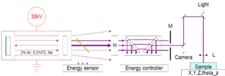
The Excimer laser ablation setup consists in an excimer laser source, the adequate optics and a 4 degrees-of-freedom positioning table allowing to program complex designs, as in the Figure 1.
The excimer gas is excited by an electric field: the resulting ultraviolet laser beam is homogenized by (H), leading to a homogeneously intense beam. A fraction of this energy can be removed by the energy controller, before the beam passes through a mask (M). The length of the optical path between the mask and the sample can be tuned in order to adjust both the focus and the demagnification (lens L) up to 14X of the image projected by the mask. The focus is done manually with the aid of a visible light beam.
The laser beam is area is around 3cm2. Depending on the demagnification rate, a mask may release one entire device, or even several ones; in this case the patterning is called static. For larger objects, a computer-aided scanning technique is employed, by accurately moving the substrate under basic mask shapes: circles, squares, rectangles etc.
The laser is pulsed with a lightening period of about 20ns, leading to cold ablation of the material: it was shown in that the kinetic energy of the ablated particle is roughly equal to the incident optical energy [15]. Therefore, thermal effects are reduced significantly with respect to YAG lasers which are not suitable for this temperature-sensitive piezoelectric material. The pulse repetition working frequency is in the order of 100Hz in order to allow a good evacuation of the ablated materials.
A classical X-Y-theta table allows manufacturing any 2D pattern. The z-axis is devoted to the focus or to manufacturing non horizontal surfaces. The total precision of the system - including the optics resolution - is on the order of a few µm.
Considering the wave length of such lasers (XeF: 351nm, KrF: 248nm, ArF: 193nm), the manufacturing is very common and efficient for polymers: a single flash can remove a layer of 300 nm, i.e the ablating speed is of the order of 0.3µm x 100Hz = 30µm/s, the aspect ratio being about 10:1. As for the PMN-PT materials, provided their high density, slower ablating rates are obviously expected. In practice, we found ablation speeds of ~2µm/s for PMN-PT, the related results will be detailed in Section 3.
2.3 Dry Etching Setup
The DRIE technique using ICP machines is well known among practitioners [10] and will not be much detailed here. Roughly, the plasma is generated within a powerful RF electromagnetic field under low pressure. Accelerating ions colide with the wafer surface and eventually react with it. The effect is a combination of chemical reaction and atomic sputtering, whose balance depends on the material and method (gas concentrations, powers, substrate temperature).
3
under different dry etching conditions. The DRIE mask deposition was performed on a regular thin Chrome buffer. Nickel is known as performing well under intensive etching energies and was chosen at the first glance. Other materials such as Cr, Al or Cu were also studied for etching masks but were later dismissed due to low selectivity, etching chamber contamination or limited deposition thickness.Finally, Ni sample masks were deposited using three different technologies: sputtering, evaporation and electroplating. The mask features (as in Fig. 3) were developed using lift-off for the sputtered samples, wet etching for evaporated ones and electroforming for the latter.
The sputtering deposition machine was a Plassys MP500 model while the evaporation one an Alliance concept Eva 450. Provided that the nickel is known for inducing residual stress during deposition, its thickness must be limited. For the sputtering technique the maximum layer cannot exceed 0.7 µµµµm. The maximum limit for evaporated Ni on PMN-PT is larger,
of around 1.5µµµµm. Finally, electrodeposited layers can be much greater, like 15 µµµµm. Under special conditions we reached an
electroplated 25 µm layer, but the sample became too constrained. On the other hand, as will be seen, etching time for such a layer would take many hours, which is expensive and un-realistic for such a process. A related graphical representation is provided in the figure 4.
2.4 Dry Etching (DRIE) Method
The ionic etching was carried out using a commercial multiplex AOE MPO 562 reactor from STS with an ICP RF generator of 3 kW and a RIE generator of 1.5 kW. The maximum size of the wafer is 6 inches, and the gas available are SF6, CF4, C4F8, He, O2 and Ar.
The temperature of the substrate holder was varied between -20 and 60°C. The gas mixture we selected was a combination Ar/C4F8 (64sccm /5sccm). The PMN-PT samples were fixed on Si carriers with thermal grease for an optimal
cooling of the sample. Step heights in µm were obtained progressively with a Tencor Alpha-step profilometer. The profiles were also measured with a scanning electron microscope (SEM) and with a MSA-500 MEMS analyzer from Polytec. This specific tool based on Michelson interferometry may offer nanometer-scale resolution in out-of-plane direction.
Dry etching parameters overview
Several combinations of etching parameters were chosen in the attempt of assessing as much data as possible from the 18 samples. Etching times varied from 30 minutes to 280 minutes.
Input parameters were as follows: - RF source power (500, 1200 W), - bias power (100, 300, 400, 500 W), - internal pressure (2, 5, 10, 15 mTorr) and - temperature (-20, 0, 60 oC).
3.
EXCIMER LASER ABLATION RESULTS
The first test searched weather the PMN-PT material may be ablated with excimer lasers, by keeping a constant frequency and raising progressively the fluence value. The results proved positive, as can be seen from the SEM images in Figure 6.
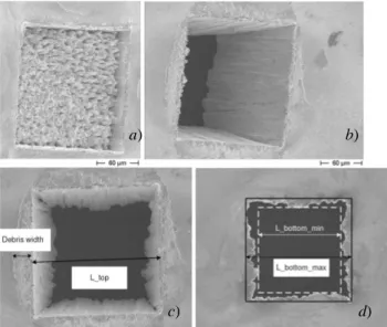
Some significant manufacturing parameters are selected and summarized in Table 1. The stabilaze value in Joule is the amount of energy contained in a laser pulse. F is the working frequency in Hertz (i.e. the repetition rate and not the laser wavelength which is fixed at 248nm according to the KrF gas mix). The column bursts indicate the number of pulses or bursts. The demagnification of the optical path is indicated with D, while the attenuator value (in %) indicates the percentage of the incident energy which goes through the energy attenuator. “Ltop” and “Lback” columns indicate the width of the ablation
(Fig. 11.c-d). Column “Debris” indicates the width of the deposition area, such as indicated in Figure 11.c. The fluence of each experiment is computed with the following formula:
Fluence = stab · D2· att/A (1)
where A = 2.33 cm2 is the laser beam area before the demagnification.
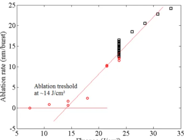
For the experiment of Table 1, the ablation rate (1m/burst) (i.e. the ablation depth divided by the number of bursts) is represented as a function of the fluence in the Figure 7 and as a function of the working frequency in Figure 8. The ablation rate increases with the fluence rate, after a threshold evaluated at 14 J/cm² which, in this case of PMN-PT is 270X higher than in the case of the polycarbonate [16]. The ablation rate (Fig. 8) is less dependent on the bursts frequency; working on higher frequencies reduces the micromachining time, however we noticed increased heating and lack of residue evacuation for frequencies above 200 Hz.
4
on the fluence value, the ablated surfaces are textured into cone-shapes of profound walls. This effect was early reported in cases where the fluence is just above the threshold [17]. In the case of PMN-PT, a difference may be observed between the textures from Figure 6. The higher the fluence, the flattened the cones become. Unfortunately, getting completely flat surfaces, as in the case of polymers, requires unrealistically powerful lasers. Even though this drawback, micromachining with excimer lasers is possible for applications of 2D cutting and drilling. A future paper will document an actuator that was cut with the excimer machine.As neither the profilometer, neither the MEMS analyser weren’t capable of measuring the trench depths, ablation rates depicted in Table 1 and in Figures 7-8 document only the profile of the cones apex. The cones base is significantly deeper into the material, as may be seen in Figure 10.
The sidewall angles were subsequently measured as they provide important means for the evaluation of the MEMS dimensional accuracy. Ideally the walls should be vertical but, as expected a slight inclination of 7° (or 83° to the horizontal) was found, which could be explained by the partial material redeposition, the beam focusing geometry etc. The data is depicted in Fig. 9 and, as seen, the sidewalls inclination is constant even for a high number of bursts.
Figure 11 depicts the successful drilling experiment of a 200µm PMN-PT plate at 23.7 J/cm² and 60 Hz. A number of 5000 pulses started perforating the plate locally. With a number of 7000 shots the hole was completely drilled, corresponding to a rate of 1.71µm/s.
4.
DRY ETCHING (DRIE) RESULTS
Mask Type dependence
Getting back to the DRIE technique, one crucial property is the etching selectivity between PMN-PT and the mask. Ni masks can be used as mask materials because of their reasonably high growth rate, typically 17µm/h for electroplated Ni. However, as the thickness of the mask increases to several micrometers, some practical challenges or disadvantages are encountered. Nickel does not react with fluorine compounds to form volatile products. In addition to the micro-masking caused by re-deposition of the non-volatiles on the area to be etched due to mechanical erosion, electroplated metals are often non-uniform in thickness (fig. 3.b). Also, thicker hard masks may introduce severe stress on the PMN-PT wafer leading to possible breakage of the mask and the PMN-PT substrate during processing. The etching speed, mask selectivity and sidewall angles were studied and displayed in Fig. 12 for electroplated, evaporated Ni and sputtered masks. For comparative reasons the same parameters combination were used during the three tests (500W bias/RF powers, 10 mTorr, 00C). While the etching speeds difference is marginal (~0.16µm/min), it was found that sputtered Ni provides better selectivity (12:1 compared to 8,3:1 for electroplated Ni). But the limiting factor of Ni sputtered mask was the difficulty to deposit Ni layers thicker than 1.51m using the lift-off. When high PMN-PT etching depths are imposed (>14µm), the electroplated masks are the only solution.
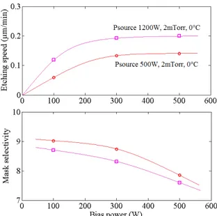
Bias power dependence
The etching rate decreases with the drop of bias and source power as in Fig. 13 (Ni evaporated mask type). In the case of a 500W source power the decrease is from 0,141m/min (Pbias 500W) to 0.061m/min (Pbias 100W). Conversely, the selectivity raises from 7,85:1 up to 9:1. In the case of the highest achievable ion source power (Psource 1200W) the etching speed increases significantly (but not proportionally) while the mask selectivity slightly deteriorates.
Microtrenches and nanometer slits
For the electroplated Ni, some micro-trenches at the bottom edge of the sidewall appeared and were attributed to a higher electron density at the edges during etching, leading to higher etching speed (Fig. 14, 15, 19). This phenomenon was already observed for quartz by Abe et al. [18] and was attributed to a bias voltage too high. Dahm et al. have also reported this effect [19] and interpreted this to a high flow of precursor gas. The main contribution for the appearance of this phenomenon is the bias voltage value.
Nanometer slits were also observed at the interface between very close structures. The phenomenon was also reported in the case of PZT [20]and is not fully understood, being attributed to material ferroelectric properties.
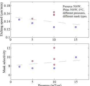
Pressure dependence
After several tries, we have found that the lowest achievable pressure (2 mTorr) of the DRIE STS machine gives slightly improved results in terms of etching speed (by 10%). The associated selectivity is however noticed to decrease from 10:1 to
5
8:1 at lower pressure values (see Fig.16).Temperature Dependence
As noticed from Fig.17 there seems no linear correlation between the etching speed and the process temperature, but the selectivity increase by several percents with the increase the temperature. This must be the result of a small release of the stress in the mask layer. Notice that we had access to the regulation of the substrate holder, which was imposed as in the Fig. 17; in reality the exposed surface heated several dozen degrees above the holder temperature, depending also on the RF/bias powers. Due to the low Curie temperature and to the mechanical fragility of PMN-PT, we recommend keeping the holder substrate temperature as low as possible.
Lateral mask etching
The etching anisotropy in terms of sidewalls angles is affected mainly by lateral mask shrinking (see Fig. 14 and 19) with lateral speeds slightly superior to the vertical ones. Because of the difficulty to asses reliable results for shallow etched surfaces, data for only electroplated mask profiles were reliable. As noticed from the figures, the lateral erosion increase with the bias power (18 nm/min at 300W and 22 nm/min at 500W).
5.
CONCLUSIONS
PMN-PT (lead magnesium niobate–lead titanate) piezoelectric material is becoming nowadays increasingly popular in various devices designs like resonant sensors, ultrasonic transducers (pMUT), micro-actuators and vibration energy harvesters designs. That is generally due to its outstanding piezoelectric properties (large coupling factors, large piezoelectric coefficients) and also to its crystalline structure, which makes it theoretically more compatible to clean room process. In this, we extensively tested the Excimer laser ablation and the inductively-coupled plasma (DRIE) etching methods on the PMN-PT material. The conclusions are as follows:
DRIE Technique Conclusions
As most piezoelectric materials, the reactive component of PMN-PT etching represents an insignificant part of the process, which mainly relies on the physical sputtering of the surface atoms due to energetic ions collisions. Therefore, we used an Ar composition, knowing that the inert gases sputter yield is higher than that of other elements or molecules (Cl2, C2H6 etc.). The material was PMN-PT [001] lapped at 200µm thickness. The Nickel
shadowing masks were electroformed at ~5.5µm or sputtered and evaporated at 0.3-0.7µm thickness.
Preliminary experience indicated the gas combination Ar(92%) + C4F8(8%). We used an STS ICP machine, a
couple dozens charts were obtained by varying different parameters (gas pressure, RF source and bias powers and the substrate temperature). An experience plan was set-up in the attempt to test the different parameters.
Various profile diagrams (e.g. the one in Fig. 18) were traced under different combinations of etching parameters, providing useful data: etching speeds, mask selectivity, sidewall angles etc.
Best achieved etching rate was 0.19 µµµµm/min with a selectivity ratio of 8:1 for 1200W source and 300W bias powers at 2 mTorr pressure. Sidewalls angles lie at ~700, mainly due to erosion of the Ni mask in lateral (horizontal) direction (Fig. 6, 9.b, 9.d). Lateral mask shrinking increased with the raise of the bias power. Expected micro-trenches at the bottom edge of the sidewall were noticed and quantified, being attributed to high local ion density at the edges during etching. Nanometer slits were also observed at the edges between structures. Compared to PZTs [13][20], (selectivity ratios of up to 35:1, etching speeds of 0.14 to 0.4 µm/min, and profile angles of ~750), we conclude that PMN-PT is slightly more renitent to dry etching than PZT. However, according to our experience, profiles of ~100 µµµµm are achievable, with the cost of
extended etching times.
Excimer Laser Technique Conclusions
A series of PMN-PT ablation tests were performed using a KrF excimer beam (248nm). Given the high material density (8200 kg/m3), the related fluence threshold was found at 14 J/cm², which is a very high value compared to the polymers. As a direct effect, ablated surfaces show material redeposition and unwanted sharp cones patterns, which, even with the maximum available demagnification and laser stabilize, were not completely fixed. However, even under such circumstances, experiments shown positive results, if we consider the cones base profile, etching rates may reach up to 100
µm/min (50 nm/pulse) which is very high compared to the DRIE results. Sidewalls verticality is of 83°, also superior to the
DRIE technique.
A paper in progress will present an actuator cut from PMN-PT with the excimer laser technique. It is found more convenient for a 2D rapid prototyping where less precise features, of around 10µm are accepted. Ionic dry etching is in
6
exchange ten times more precise but is time-consuming and requires a hard mask deposition. DRIE surfaces are noticeably flatter and cleaner, without debris particles deposition.ACKNOWLEDGEMENTS
We express our gratitude to Frédérik Cambier for allowing us to work on the excimer laser machine of Techifutur (Liège, Belgium).
The work was supported under the EU grants FP7-PEOPLE-IEF 219412/2007 – MicroPAdS and FP7-PEOPLE-RG 276991/2010– MICROGENS.
REFERENCES
[1] F. Wang, L. Luo, D. Zhou, X. Zhao, H. Luo, “Complete set of elastic, dielectric and piezoelectric constants of orthorhombic 0.71Pb(Mg1/3Nb2/3)O3-0.29PbTiO3 single crystal”, Appl. Phys. Lett. 90, 212903, 2007
[2] R. Zhang, B. Jiang, W. Cao, “Complete set of material constants of 0.93Pb(Zn1/3Nb2/3)O3-0.07PbTiO3 domain engineered single crystal”, J. of Mat. Sci. Lett. 21, pp. 1877-1879, 2002.
[3] J.R. Yuan, X. Jiang, K. Snook, P.W. Rehrig, T.R. Shrout, W.S. Hackenberger, A. Cheng, P. Cao, G. Lavelelle, X. Geng, “Microfabrication of Piezoelectric Composite Ultrasound Transducers (PC-MUT)”, Proc. 2006 IEEE Ultras. Symp., pp. 922-925, 2006.
[4] S. Hur, S. Q. Lee, H. S. Choi, “Fabrication and characterization of PMN-PT single crystal cantilever array for cochlear-like acoustic sensor”, J. Mech. Sci. Tech. 24, No.1, 181-184, 2009
[5] S. Tadigadapa and K. Mateti, “Piezoelectric MEMS sensors:state-of-the-art and perspectives”, Meas. Sci. Technol. 20 092001 (30pp), 2009
[6] I. A. Ivan, M. Rakotondrabe, J. Agnus, R. Bourquin, N. Chaillet, P. Lutz, J-C. Poncot, R. Duffait, O. Bauer, “Comparative material study between PZT ceramic and newer crystalline PMN-PT and PZN-PT materials for composite bimorph actuators” Rev. Adv. Mat. Sci. Vol.24, No2 , pp.1-9, 2010.
[7] W. Pfleging, M. Przybylski, H.J. Bruckner, "Excimer laser material processing - State of the art and new approaches in microsystem technology", Conference on Laser-Based Micropackaging, Proc. of SPIE Vol. 6107, pp. G1070, San Jose, CA, 2006
[8] J-P. Desbiens, P. Lasson, “ArF excimer laser micromachining of Pyrex, SiC and PZT for rapid prototyping of MEMS components”, Sensors and actuators: A, Physical, vol. 136, no2, pp. 554-563, 2007
[9] J. Lappalainena, J. Franttia, H. Moilanena, S. Leppävuoria, “Excimer laser ablation of PZT thin films on silicon cantilever beams”, Sensors and Actuators A: Physical, Volume 46, Issues 1-3, Pages 104-109, 1995
[10] S.M. Rossnagel, J.J. Cuomo, W.D. Westwood, “Handbook of Plasma Processing Technology - Fundamentals, Etching, Deposition, and Surface Interactions”, William Andrew Publishing/Noyes, 1990
[11] S. Schreiter and H.U. Poll, “A new plasma-etching technique for micromechanical structuring of quartz”, Sensors Actuators A, vol. 35, pp. 137–141, 1992
[12]F.A. Khan, L. Zhou, V. Kumar, I. Adesida, R. Okojie, “High rate etching of AlN using BCl3/Cl2/Ar inductively coupled plasma”, Mater. Sci. Eng B 95 pp. 51–54, 2002
[13]A. M. Efremov, D.P. Kim, K.T. Kim, C.I. Kim, “Etching characteristics and mechanism of Pb(Zr,Ti)O3 thin films in CF4/Ar inductively coupled plasma”, Vacuum vol. 75, issue 4, pp. 321–329, 2004
[14]J. Agnus I. A. Ivan, S. Queste, “Dry etching of single crystal PMN-PT piezoelectric material”, IEEE MEMS Conference, ISBN 978-1-4244-9633-4, pp. 237-240, Cancun, Mexico, 2011
[15]K. Naessens, “Eximer laser ablation of microstructures in polymers for photonic applications”, PhD thesis, Universiteit Gent, 2004.
[16]J. Kruger H. Niino and A. Yabe, “Investigation of excimer laser ablation threshold of polymers using a microphone”, Applied surface science, vol. 197-98, pp. 800-804, 2002
[17]E. van de Riet, C. J. C. M. Nillesen, J. Dieleman, “Reduction of droplet emission and target roughening in laser ablation and deposition of metals”, Journal of Applied Physics, Volume 74, Issue 3, pp.2008-2012, 1993
[18] T. Abe and M. Esashi, “One-chip multichannel quartz crystal microbalance (QCM) fabricated by Deep RIE”, Sensors and Actuators 82, pp. 139-143, 2000.
[19]G. Dahm, I.W. Rangelow, P. Hudek and H.W.P. Koops, “Quartz etching for phase shifting masks”, Microelectronic Engineering 27, pp 263-266, 1995.
[20]S. Wang, X. Li, K. Wakabayashi, M. Esashi, "Deep Reactive Ion Etching of Lead Zirconate Titanate Using Sulfur Hexafluoride Gas" J. Am. Ceram. Soc., 82 pp. 1339–1341, 1999
7
BIOGRAPHIES
Ioan Alexandru Ivan is a research engineer to the French institute FEMTO-ST where he carried-out an FP7 Marie Curie
project called MicroPAdS. In parallel he is an electrical engineering lecturer at Valahia University from Romania. He is a physics engineer of the University of Bucharest and a Ph.D. in microelectronics from the University of Besançon, since 2006. His actual research interests are in various piezoelectric micromechatronic systems, PMN-PT materials included.
Joël Agnus received the Master of Science in Electrical Engineering in 1994 and the Ph.D degree in Automatic Control and
Computer Sciences from the University of Besançon, France, in 2003. He is an engineer involved in microrobotics field, and more particular concerning microgrippers, piezoelectric material and force sensors within micromanipulation domain.
Pierre Lambert received a Master in Engineering Sciences in 1998 and a PhD in 2004 from the Université Libre de
Bruxelles (ULB). He has been an Assistant Professor in ULB since 2006 and a CNRS senior scientist since 2009. He’s involved in studying surface tension effects in Microsystems, with a focus on capillary forces and micro-engineering. In 2010-2011, he has been a visiting researcher in University of Tokyo.
Note: Table 1 is in a separate PDF file Thank you for your reviewing!
8
Figure 1. The excimer laser ablation micromachining unit.
Figure 2. Photography of an excimer-ablated sample, notice that some holes are completely perforated. The halos around the holes are caused by some ablated material redeposition (larger for the drilled holes, as the the PMMA glass underneath was subsequently ablated).
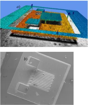
Figure 3. a) One PMN-PT sample electroplated with an arbitrary Nickel hard mask. Notice the PMN-PT is translucent. b) One SEM image detail of the bottom-left pinion gearwheel.
Figure 4. Typical DRIE etching diagram of PMN-PT recorded with a profilometer, allowing the evaluation of the etching rate and selectivity. For the given example the mask was 0.7 µm-thick evaporated Ni. Six experimental points were recorded during the 55’ process allowing to derive the etching speed and the mask selectivity.
b) a)
10
Figure 5.a) A dry-etched feature in PMN-PT imaged by 3D measurement software TMS 3.1 installed on a MSA-500 analyzer.
b) Same sample imaged by SEM.
Figure 6. SEM images of ablated PMN-PT samples with 300 pulses at 3 Hz. Different energy values: 6.5 J/cm² (below fluence threshold), 11 J/cm², 19 J/cm² and 23.5 J/cm² respectively. Images are inclined by 30°.
a) b) a) b) c) d) 19 J/cm² 23.5 J/cm² 6.5 J/cm² 11 J/cm²
11
Figure 7: Ablation rate as a function of the excimer laser fluence. Note1: The circles and squares denote two different experience plans conducted in lower and higher fluence. Note2: measurements performed with a mechanical profilometer: the tips cones apex are convoluted with the 45° profilometer cantilever. Cones base is more profound.
Figure 8: Ablation rate as a function of the bursts frequency. The red circles dots were recorded in various low fluence conditions, while the black squares denote higher fluences. The vertical dispersion of the 60 Hz points is due to the different beam energies (higher fluence – higher ablation rate). As for the points above 80 Hz, smaller dispersion is observed due to the more constant fluence values (around 24 J/cm2).
Figure 9: Influence of the number of bursts on the inclination of the flanks. The angle is given with respect to the vertical axis.
12
Figure 10. SEM image of the ablated PMN-PT in cross-section. The cone-structure is visible. The cones height in the figure vary from 15µm to 30µm.
Figure 11. Drilling experiment of a 200 µm PMN-PT plate. Parameters: KrF laser (248nm), fluence 23.7 J/cm² , frequency 60Hz. a) SEM picture after 1000 impulses (17 seconds), image is inclined by 30°, cones are visible. b) SEM picture after 7000 shots (117 s), image is inclined by 30°, showing that drilling of the plate is achieved. c) Top vertical image of the drilled plate. d) Bottom image and quantities allowing estimating the sidewalls verticality.
Figure 12. Comparative PMN-PT etching results for electroplated, evaporated and sputtered Ni masks. ICP parameters: 500/500W, 10 mTorr, 00C, Ar/C4F8 (64/5).
a) b)
13
Figure 13. Etching speed and selectivity vs. bias and source power.
Figure 14. Effects of increased bias power (right): notice larger microtrenches, larger lateral mask erosion, presence of nanometer slits (arrows)
Figure 15 Detail on dry etching of PMN-PT. Notice the microtrenching and mask shrinking effects. Some evaluation quantities are depicted.
14
Figure 16. Selectivity vs. pressure (different param.)
Figure 17. Etching speed and selectivity vs. holder temperature.
Figure 18. Typical etching profiles and speed diagram (Psource 500W, Pbias 500W, 10mTorr, Temperature 0°C). The related SEM images at 130 and 280 minutes (intermediate and end point) are depicted in fig. 19.
15
Figures 19 a,b). Zoomed SEM images taken at 130’: lateral Ni mask erosion is in progress, profile is 26 um deep.
Figures 19 c,d). Same features etched after 280’: profile is 47 um deep, notice the complete erosion of Ni mask (fig 9.d, except for the intersections) Sidewalls rugosity and micro-trenches are increased. Ni lateral erosion.
a) c)