HAL Id: tel-02384928
https://tel.archives-ouvertes.fr/tel-02384928
Submitted on 28 Nov 2019HAL is a multi-disciplinary open access
archive for the deposit and dissemination of sci-entific research documents, whether they are pub-lished or not. The documents may come from teaching and research institutions in France or abroad, or from public or private research centers.
L’archive ouverte pluridisciplinaire HAL, est destinée au dépôt et à la diffusion de documents scientifiques de niveau recherche, publiés ou non, émanant des établissements d’enseignement et de recherche français ou étrangers, des laboratoires publics ou privés.
fabricated on flexible substrate
Hanpeng Dong
To cite this version:
Hanpeng Dong. Microcrystalline silicon based thin film transistors fabricated on flexible substrate. Electronics. Université Rennes 1, 2015. English. �NNT : 2015REN1S173�. �tel-02384928�
THÈSE / UNIVERSITÉ DE RENNES 1
sous le sceau de l’Université Européenne de Bretagnepour le grade de
DOCTEUR DE L’UNIVERSITÉ DE RENNES 1
Mention : ElectroniqueEcole doctorale MATISSE
présentée par
Hanpeng Dong
Préparée UMR-CNRS 6164 IETR
Institut d’Electronique et de Télécommunications de Rennes
UFR ISTIC
Intitulé de la thèse :
Microcrystalline
silicon based Thin
Film Transistors
fabricated on Flexible
Substrate
Thèse soutenue à Rennes le 25 septembre 2015
devant le jury composé de :
Yvan BONNASSIEUX
Professeur, Ecole Polytechnique Palaiseau /
rapporteur
François TEMPLIER
Ingénieur HDR CEA-LETI MINATEC / rapporteur
Takashi NOGUCHI
Professeur, Université Okinawa Japon /
examinateur Lei WEI
Professeur, Université South-East Nanjing Chine /
examinateur
Emmanuel JACQUES
Maître de Conférences Université Rennes 1 /
examinateur
Tayeb MOHAMMED-BRAHIM
1
2
Introduction………7
Chapter 1 Microcrystalline silicon thin film transistors: Applications and technologies…..11
1. Introduction ... 12
2. Low temperature TFTs for display applications ... 12
2.1 TFTs for liquid crystal display ... 12
2.2 TFTs for OLED ... 15
2.3 Quantum-dot light emitting display (QLED) ... 17
3. TFTs for Flexible electronics ... 18
3.1 Flexible displays ... 18
3.2 Flexible sensors ... 20
3.3 RFID tags ... 21
4. Different flexible substrates ... 22
4.1 The thin glass ... 23
4.2 Flexible stainless steel foil ... 23
4.3 Paper substrate ... 24
4.4 Plastics ... 24
4.5 Conclusion ... 25
5. State-of-the-arts of low temperature TFTs ... 26
5.1 Organic thin film transistors ... 27
5.2 Oxide semiconductor thin film transistors ... 29
5.3 Silicon thin film transistors ... 31
5.3.1 Amorphous silicon thin film transistors ... 31
5.3.2 Low-temperature polycrystalline silicon (LTPS) thin film transistors ... 32
3
6. Conclusion ... 38
References ... 40
Chapter 2 Technologies for the microcrystalline silicon TFT fabrication………..51
1. Introduction ... 52
2. Deposition technologies and material properties for the realization of low temperature microcrystalline silicon thin film transistor ... 53
2.1 Undoped and doped microcrystalline silicon ... 53
2.1.1 Deposition of undoped and doped microcrystalline silicon film ... 53
2.1.2 Material properties of undoped and doped microcrystalline silicon ... 55
2.1.2.1 Undoped microcrystalline silicon ... 55
2.1.2.2 N-type doped microcrystalline silicon ... 58
2.2 Deposition of gate insulator ... 59
2.2.1 Silicon oxide deposited by sputtering ... 60
2.2.2 Silicon oxide deposited by ECR-CVD ... 61
2.2.3 Alumina deposited by ALD ... 62
2.2.4 Silicon nitride deposited by PECVD ... 64
3. Technologies for thin film characterization ... 65
3.1 Thickness measurement by profilometer ... 65
3.2 Roughness and morphologies measurement by AFM ... 66
3.3 Scanning electron microscopy (SEM) ... 67
3.4 Measurement of the electrical conductivity ... 67
3.5 Measurement of the crystalline fraction of microcrystalline silicon by Raman spectroscopy ... 69
4. Fabrication of microcrystalline silicon thin film transistor ... 71
4.1 Preparation of substrate ... 71
4
4.3 Deposition of doped microcrystalline silicon ... 72
4.4 Definition of channel area (Mask 1) ... 72
4.5 Definition of TFT geometry (Mask 2) ... 73
4.6 RCA cleaning of the silicon surface ... 73
4.7 Deposition of gate insulator ... 74
4.8 Gate insulator etching for source and drain contact (Mask 3) ... 75
4.9 Deposition of aluminum and definition of source, drain and gate electrode. (Mask 4).... 76
5. Basic working principle and characterization of microcrystalline silicon TFTs ... 77
5.1 Basic working principle of TFTs ... 77
5.1.1 Linear regime ... 78
5.1.2 Saturation regime ... 79
5.2 TFTs electrical characteristics ... 80
5.2.1 Transfer characteristics ... 80
5.2.2 Output characteristics ... 81
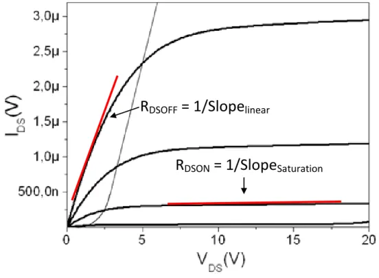
5.3 Extraction of characteristics parameters ... 81
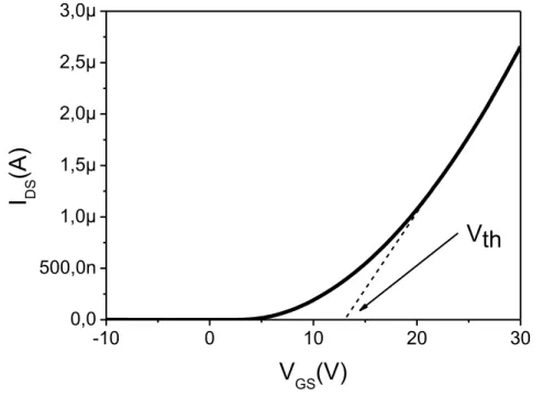
5.3.1 Threshold voltage: ... 81
5.3.2 Field effect mobility ... 83
5.3.3 Subthreshold slope ... 84
5.3.4 The ION/IOFF and RDSON/RDSOFF ratio ... 85
6. Conclusion ... 86
References ... 88
State-of-the-art and problematic of microcrystalline silicon TFT technology in IETR laboratory………..91
References ... 97
5
1. Introduction ... 100
2. TFTs fabricated at low temperature compatible with the use of transparent flexible substrate ... 100
2.1 Electrical characterization of TFTs ... 100
2.2 Electrical stability of microcrystalline silicon TFTs ... 102
2.2.1 Threshold voltage shift models ... 103
2.2.2 Gate bias stress for microcrystalline silicon TFTs ... 106
2.2.3 Conclusion on the electrical stability of microcrystalline silicon TFTs using silicon nitride as gate insulator ... 112
3. Microcrystalline silicon TFTs on flexible substrates ... 113
3.1 Fabrication of microcrystalline silicon TFTs on PEN substrate. ... 114
3.1.1 Strain calculation ... 114
3.1.2 TFT’s process ... 119
3.1.3 TFT’s electrical characterization ... 119
3.2 Mechanical behavior of microcrystalline silicon TFTs on PEN substrate... 122
3.2.1 Mechanical stress tools ... 122
3.2.2 TFTs behavior during bending tests ... 123
3.2.3 TFTs critical radii under tension and compression ... 125
3.2.4 TFTs reliability under multiple bending ... 126
3.2.5 Discussion of the high flexibility of microcrystalline silicon TFT on PEN substrate ... 128
4. Conclusion ... 129
References ... 131
Chapter 4 Increasing the mobility of microcrystalline silicon TFT………...135
1. Introduction ... 136
6
2.1 RF sputtered silicon dioxide as gate insulator ... 136
2.1.1 Reviews of previous TFTs using silicon oxide deposited at ambient temperature (without heating the substrate) by RF sputtering ... 137
2.1.2 Silicon dioxide deposited at fixed temperature RF sputtering ... 138
2.1.2.1 MOS capacitance using SiO2 deposited at 150°C ... 138
2.1.2.2 TFTs using SiO2 deposited at 150°C and then annealed at 250°C during 1h under forming gas. ... 141
2.2 TFTs using ECR-CVD deposited SiO2 as gate insulator ... 143
2.3 TFTs using ALD deposited Al2O3 as gate insulator ... 145
2.4 TFTs using PECVD deposited Si3N4 as gate insulator ... 150
2.4.1 Transfer characteristic of TFTs using multilayer silicon nitride as gate insulator ... .151
2.4.2 TFTs using multilayer silicon nitride as gate insulator under prolonged gate bias stress ... 152
3. Conclusion ... 154
References ... 156
Conclusion………...157
7
8
Flexible electronic is a novel challenge for the electronic market and attract numerous research laboratories and industrial companies. The main applications of flexible electronic include rollable displays (LCD, OLED and EPD), RFID tags and flexible sensors. Beside low temperature compatible with flexible substrate, these applications require also high field effect mobility, good electrical stability and high flexibility of thin film transistors (TFT). However, the conventional amorphous silicon TFT (a-Si:H TFT) used for industry TFT-LCD has well-known drawbacks as low field effect mobility and poor electrical stability. Therefore, several novel low temperature TFT technologies such as organic TFTs, metallic oxide TFTs and crystalline silicon TFTs have been emerged in order to obtain better electrical performances.
All these technologies have their advantages and drawbacks. Organic TFTs (OTFT) can have extreme flexibility and can be fabricated with several low-temperature technologies such as evaporation, spin-coating or inkjet-printing. Their mobility has been largely increased in the recent years. But TFTs are still suffered from several problems. Metallic oxide TFTs provide very high mobility. The metallic oxide semiconductors are transparent and can be deposited at low temperature. But before their commercialization, the electrical instability under the positive or negative bias stress should be carefully studied. Low temperature polycrystalline silicon (LTPS) TFTs have high mobility and good electrical stability, but laser crystallization increases their fabrication cost and limits their uniformity. The present work focuses on the microcrystalline silicon technology. In IETR laboratory, microcrystalline silicon technology on glass and plastic substrates has been developed. The deposition has been performed at a temperature lower than 180 °C in order to be compatible with plastic substrate such as PEN. These flexible and transparent substrates are provided by DuPont Teijin Film. Precedent works in IETR have already demonstrated the possibility to fabricate microcrystalline silicon TFTs on this PEN substrate. This thesis deals with the improvement of field effect mobility, electrical stability and mechanical flexibility of these TFTs. The organization of this thesis is shown below:
In the first chapter, the state-of-the-art for flexible electronic applications will be introduced. Flexible displays, RFID tags and flexible sensors will be described. Afterwards,
9
different flexible substrates used for these applications will be presented. Their properties such as maximum process temperature, transparency and mechanical flexibility will be detailed. Finally, different low-temperature TFT technologies, including organic TFT, metallic oxide TFT and silicon TFT, will be presented by discussing their semiconducting principles, electrical performances and limitations.
In the second chapter, the fabrication process of microcrystalline silicon TFTs will be described. First, the technologies of thin film materials (especially for undoped microcrystalline silicon) deposition and characterization will be detailed. Afterwards, an introduction of microcrystalline silicon TFTs technology will be given. This introduction includes the fabrication steps, the basic working principles and characterization of TFTs. and will be finished by the electrical characteristics of microcrystalline silicon TFTs on glass and on plastic substrate presented by previous works in IETR.
Before the third and fourth chapter, a state-of-the-art and problematic of microcrystalline silicon TFT technology will be presented. This short introduction will summarize the previous works on flexible microcrystalline silicon TFT and give the motivation of the studies in the third and fourth chapter.
In the third chapter, electrical stability and mechanical flexibility of microcrystalline silicon TFTs will be studied. Firstly, the TFTs will be fabricated on glass substrate. They will be electrically stressed under different gate voltages at different temperatures in order to explain the mechanism of electrical characteristics shift of TFTs. Secondly, the TFTs will be fabricated on PEN substrate. They will be electrically characterized during mechanical bending, for both tension and compression for different curvature radii. The variation of their electrical characteristics under mechanical bending will be studied and discussed. The minimum curvature radius of TFTs will be also determined in this part. Moreover, the method to obtain lowest possible curvature radius of TFTs will be discussed in the end of this chapter.
In the fourth chapter, the microcrystalline silicon TFTs will be fabricated with different gate insulator materials in order to increase field effect mobility of TFTs. The gate insulator materials include silicon oxide deposited by sputtering and ECR-CVD, alumina deposited by
10
thermal ALD and silicon nitride deposited by PECVD. Electrical characteristics of TFTs using these gate insulators will be presented and discussed. The possibility of increasing field effect mobility of microcrystalline silicon TFTs to at least 5 cm²/Vs, which is the mobility needed for AMOLED, without sacrificing electrical stability, will be discussed at the end of this chapter.
11
Chapter 1: Microcrystalline silicon thin film
transistors: Applications and technologies
12
1. Introduction
The display industry has benefited from a large development in the past 20 years. Today‟s display devices trend to be more bright, flat, with high resolution and efficient. The flexible displays fabricated on the plastic or paper substrate, turned out to be a very interesting target for the future. Moreover, the other applications of flexible electronics, such as RFID and flexible sensors, have attracted large attention of numerous research laboratories supported by industries. To fabricate electronic devices on flexible substrate which could not be maintained at high temperature, there are 2 different types of technologies. The first one is to fabricate devices on glass or silicon substrate and then transfer to flexible one (paper, plastic). For this method, the low temperature fabrication is not necessary but the cost is higher. The second one is to fabricate directly on the flexible substrate. For these technologies, a low temperature thin film transistor (TFT) technology compatible with such substrate, without sacrificing electrical or mechanical performance, is needed. With this background, several novel low temperature TFT technologies such as organic TFTs, metallic oxide TFTs and silicon TFTs have been emerged envisaging the challenge of commercialization, not only for flexible displays, but also for the other applications of flexible electronics. These TFT technologies have different mechanisms, performances, advantages and drawbacks. In this chapter, the applications and the properties of such low temperature TFT technologies are introduced.
2. Low temperature TFTs for display applications
2.1 TFTs for liquid crystal display
The TFT LCDs have superiors performances compared to CRT (cathode ray tube) displays in terms of flatness, lightness, and low power consumption. LCD has replaced CRT and became the leading display technology in recent year .
The configuration of a LCD display panel is shown in figure 1.1 [1]. The Liquid crystal is deposited between the two polarization panels, one is covered by uniform conductive layer while another is covered by the TFT matrix. The TFT matrix containing lines and columns
13
plays an important role in the LCD operation. The TFTs are located between each line and column respectively to control the LC pixel. The TFT is also connected with a capacitance. So the role of TFT is: (1) in the on state of TFT, data current goes though the TFT to drive the liquid crystal of each pixel. (2) In the off state of TFT, the voltage applied on the liquid crystal in the passing state is kept by the capacitor until all the pixels are addressed. Figure 1.2 shows typical structure and manufacturing process of TFT matrix for LCD display [2]. To drive a LCD display panel, the voltages should be applied on the lines and columns following a regular timing. As shown in Figure 1.3, when a positive voltage (should be superior to the threshold voltage of TFT) is applied to the gate electrode, which is connected to the scan line, TFT will be turned on. Then the data voltage can be delivered from data line to LC and storage capacitor. On the other hand, if there is no voltage applied to the scan line, the TFTs are in their blocked state. The charges kept in the capacitors, which are connected with the drain of TFTs, can make a conservation of precedent pixel image.
Figure 1.1: Structure of TFT-LCD [1]
For high resolution or large area LCD displays, high mobility of TFT is needed to maintain the display quality because of the short response time required for each pixel. With high mobility, charge carriers can move easily in the device to make a reduction of delay time of pixel refreshing. High stability and good uniformity are also demanded for the display long-term reliability and for the large size display, respectively.
14
Figure 1.2: Typical TFT matrix structure and manufacturing process [2]
Figure 1.3 Pixel circuit for TFT-LCD [3]
Today, most of industrial productions of TFT-LCD displays are based on hydrogenated amorphous silicon (a-Si:H). They are inexpensive, reliable, and can be fabricated at low temperature [4]. However, the application of a-Si:H TFTs in the large area devices is limited by their low carrier mobility and their threshold voltage shift. Therefore, alternative TFT technologies with higher carrier mobility and electrical stability are needed. In the recent years, organic TFT, metallic oxide TFT, low temperature poly-silicon TFT (LTPS TFT) and
15
microcrystalline silicon TFT (µc-Si TFT) technologies have been developed. Their features and advantages will be detailed thereafter.
2.2 TFTs for OLED
With their high brightness, low power consumption, wide viewing angle and so on, OLEDs make themselves a leading next-generation technology compared to the other flat panel displays [5]. Moreover, an active-matrix OLED (AMOLED) has lower power consumption and faster refresh rate than other driving system.
The structure of OLED unite is shown in figure 1.4 [6]. The organic material is sandwiched between two conductors (anode and cathode). When a voltage is applied on the electrodes, electrons are injected from cathode and holes are injected from anode. The recombination of electron-hole is taken place into the emissive layer and release energy to produce the light.
Figure 1.4: OLED unit pixel structure [6]
Since the luminance of OLED is proportional to the driving current, two TFTs at least are needed in order to supply a constant current during each frame period. Figure 1.5 shows a conventional pixel structure [7]. One transistor (T1) is switched on to charge a capacitor and the other (T2) deliver a constant current from the capacitance voltage to illuminate the pixel. In most of researches, more complicated pixel circuits are always designed using 3 TFTs, 4 TFTs and even more. (Figure 1.6) [8]. The TFT should have long-term stability under bias
16
stress and ambient environment. Electrical instability could lead to a threshold voltage shift that causes a reduction in the pixel luminance. In addition, the high mobility of TFT is also needed to realize a large size OLED display.
Figure 1.5: AMOLED conventional 2-TFTs pixel structure [7]
Figure 1.6: A 3-TFTs OLED pixel structure [8]
The a-Si:H TFT AMOLED suffers from their low carrier mobility and high threshold voltage shift which are related to the display degradation. One method to solve this problem is to use more complicated configurations. This way leads to an increase of electronics devices surface. The aperture ratio, which means the ratio of electronic device surface to total display surface, is thus sacrificed. In addition, an alternative technology with higher mobility and mainly better stability are needed. The µc-Si TFT could be an alternative technology. Indeed, we demonstrated the possibility to use µc-Si TFT in an AMOLED circuit with Thomson R&D France [9].
17
2.3 Quantum-dot light emitting display (QLED)
Since the first report in 1994 [10], quantum-dot LEDs have attracted much attention in the past years. Thanks to their unique properties, such as solution process [11], low energy consummation, compatibility with flexible substrate, tunable emitting wavelength over the entire visible spectrum [12] and improved color saturation, the quantum-dot LEDs become an interesting candidate for the application of thin film displays.
The mechanisms of quantum-dot light emitting diode (QLED) and OLED are very closed. The only difference is the material used as the active luminescent layer. For OLED display, organic material is used as the luminescent layer. For the QLED display, the luminescent layer is made of particularly treated II- VI or III-V component based semiconductor. Figure 1.7 shows an example of a blue QLED device.
Figure 1.7: Structure of blue quantum-dot LED [13]
In this structure, the ZnCdS/Zns quantum dot (QDs) is used as active luminescent layer. The ZnO NPs, PVK and PEDOT:PSS are used as electron transport , hole transport and hole injection layer, respectively. In the other report, CdSe/Cds QDs [14] and ZnCdSeS QDs [11] have been used as QDs luminescent layer. In the common QDs fabrications, different QDs size can be obtained by controlling the reaction temperature and time. Moreover, the band-gap of QDs is governed by their size. Therefore, size-controlled tunable light emitting can be achieved. This might be the most interesting property of QLED device.
18
Since their first report in 1994 [10], the light emitting efficiency of QLEDs has been increased by a factor of more than 1800, from less than 0.01% to around 18% [Yasuhiro Shirasaki Nature Photonics 7 13-23 (2013) ], which are comparable tothose of OLEDs. The major challenge is their lifetime. Today‟s QLEDs lifetime at the initial brightness can reach 1,000 hours while more than 10,000 hours is needed for displays.
The Southeast University of Nanjing, China, has begun their studies on QLEDs very recently. They developed an all solution-processed method to fabricate blue and green QLEDs by optimizing the thickness of all the electron transport, the hole transport and the hole injection layers [11]. The collaboration between Southeast University and University of Rennes 1gives us a possibility to carry out on a novel TFT application: the QLED display addressed by microcrystalline silicon TFT fabricated at low temperature.
3 TFTs for Flexible electronics
3.1 Flexible displays
The flexible displays have been extensively studied by a large number of electronics manufacturers to transfer this concept to the market in the recent years. A lot of flexible display production has begun to enter into our horizon. In 2005, Arizona State University created a flexible display center by receiving 43.5 million dollars from Army Research Lab. With Hewlett Packard, their partnership, they have presented a flexible e-paper [15]. In 2010, Samsung has begun to develop a 4.5-inch flexible AMOLED and try to start mass production of this kind of displays. On 8 October 2013, they announced the world‟s first flexible-display phone that carries a 5.7-inch touchscreen with a resolution of 1080×1092 [16]. However, this kind of screen cannot be strictly seen as „flexible‟, but merely „bendable‟ displays. In the underside of figure 1.8 is the 4.1-inch rollable OLED displays reported by Sony [17].
19
Figure 1.8: Applications of flexible displays. a) Electronic paper by HP and ASU [15]. b) Smart phone by Samsung [16]. c) Rollable screen by Sony [17].
The development of low temperature TFT is also a key issue for the progress of flexible displays. The low temperature fabrication makes plastics possible as substrate of flexible display. In many research laboratories, flexible displays using low temperature fabricated TFT have been reported. For flexible OLED displays, the organic TFTs and silicon TFTs have been used since more than 10 years [18, 19]. These flexible displays present matrix with low pixel resolutions. Recently, as the device fabrication technologies have been well developed, some research laboratories demonstrate their flexible TFT with higher resolution [20, 21]. The electrical and mechanical stabilities of these TFTs are also improved. Indeed, the mobility and the flexibility of TFTs, especially for organic TFTs, have been largely improved based on numerous efforts of researchers.
20
Figure 1.9 Flexible displays in research laboratories: a) OLED using a-Si:H TFTs on metal foil substrate [18], b) OLED using bottom gate OTFTs on plastic substrate [19], c) EPD using
solution-processed OTFT [20], d) Flexible OLED device [21].
3.2 Flexible sensors
The flexible sensors are also important in flexible electronics. The main flexible sensors include the bio-chemical sensors, the medical patches, the artificial skin and other as temperature, pH and gas sensors. A research group has developed a flexible chemical sensor [22, 23]. This sensor is based on bottom gated TFT using SWNTs (Single-Wall Carbon Nanotube) as active layer. The sensor is stable when functioned in the water. The high sensitivity of the sensor permits the detection of poison in water or explosive compounds such as TNT (Figure 1.10 a)). Another application field is the artificial skin. In 2013, C. Wang et al [24] presented a user-interactive electronic sensor. During their experiment, finger pressure upon surface of sample can be detected and visualized by illuminating OLED pixel on the opposite side of sample. The light intensity corresponds with the pressure. A
a)
b)
21
research group at Tokyo University has developed a matrix based on organic TFT sensors [25]. This tactile sensor can be used for health care and monitoring (Figure 1.10 c). The organic TFTs used for the sensor matrix has extreme flexibility (Figure 1.10 d). They maintain stable function even after some extreme bending conditions such as bending curvature radius of 5µm within the active area and tensile strain of 233%.
Figure 1.10 Different types of flexible sensors: a) chemical compound sensor [22], b) user-interactive electronic skin [24], c) and d) ultra-flexible organic TFT sensor [25].
3.3 RFID tags
The RFID tag (Radio Frequency Identification) is a wireless system used for the identification with certain distance using electromagnetic signal. The data of an item or an animal can be saved inside the RFID tag with electromagnetic format. Then a special reader will be used to identify it. The RFID is used like a barcode but the RFID is not necessary to be in the sight of the reader.
Now, two types of RFID exist: active RFID and passive RFID. The active RFID has a local power source like a battery, which supplies the power consummation for reading or
a)
b)
22
writing data. Therefore, the data of an active RFID can be modified. On the other hand, the power source, which is need to be inside the active RFID, makes the flexible devices more expensive.
The second type, passive RFID, need to be powered by electromagnetic fields produced by or near the reader. The battery-free passive RFID is possible to be flexible. Figure 1.11 presents simplified schema of a RFID system. This system is composed by 3 parts: RF antenna, rectifier and CMOS circuit. The RF antenna is used for the communication between reader and RFID by sending or receiving RF signal. Then the AC signal is converted to DC signal by rectifier. The CMOS circuit, which has some oscillators and logic gates, will save the converted DC signal.
Figure 1.11 Simplified schema of RFID
Recently W. Huang et al [26] integrated RFID and flexible sensor technologies by realizing a passive RF pH-sensor. The flexible pH-sensor tag can measure the pH value in food and the data can be sent to a reader (computer terminal) by RF technology. This kind of devices provides an open way for the researchers to further exploration of novel and interesting applications based on flexible electronics.
4. Different flexible substrates
There are mainly 4 types of different flexible substrates for the flexible electronics devices: thin glass, stainless steel foil, plastic and paper. The choice of substrate is depending on the application. For example, the flexible displays require the substrate to be transparent. For the flexible display applications, the surface quality of substrate is also needed to be sufficient.
23
On the other hand, the low-cost substrate is needed for some disposal electronics. To choose a flexible substrate, these factors are generally considered:
The maximum temperature that substrate can hold. The thermal expansion coefficient of substrate The transparency
The cost
The surface roughness
The robustness with environment
4.1 The thin glass
The glass will be flexible when its thickness reduced less than 200 μm [27]. Some commercialized thin glass‟s thickness can be reduced until 25 μm [28]. The main advantages of thin glass as flexible substrate include the quasi-perfect surface with roughness normally less than 0.5 nm, the high optical transparency, the high process temperature without thermal deformation, the impermeability of water or oxygen and the high chemical resistance. Benefiting from these properties, the TFTs or LCD and OLED can be fabricated on thin glass substrate with high performances. For example, S. M. Garner et al [29] present a high-quality and high-resolution electrophoretic display driven by organic TFT on flexible glass substrate. Benefit from the high quality of glass surface, the organic TFTs are electrically stable. S. Hoehla et al [30] use 75-µm-thick flexible glass for an active matrix LCD display. The TFTs have been directly fabricated on the glass substrate without degradation compared to the TFTs fabricated on thicker glass. On the other hand, the main drawback of thin glass substrate is its fragility and the high fabrication cost.
4.2 Flexible stainless steel foil
The flexible stainless steel foils have normally a thickness around 100 μm. They are impermeable to oxygen and water. They can be processed at high temperature without deformation. They also offer high mechanical strength. Therefore, the TFTs fabricated on flexible stainless steel foil are suitable for some high performance and/or large area
24
applications. For example, T. Serikawa and F. Omata [31] reported poly-Si TFTs on flexible stainless steel foil. The silicon is crystallized by excimer laser and has high mobility of 106 cm²/Vs. D. Jin et al [32] demonstrated a very thin AMOLED display based on LTPS TFT which has a mobility of 71.2 cm²/Vs. High quality display images have been shown in this work. The main drawback of flexible stainless steel foil is its opacity, the need of encapsulation layer due to its conducting nature and the high surface roughness. The opacity restricts its applications in certain situation in which transparency of substrate is required. The need of encapsulation or planarization layer limits the maximum temperature of process. Moreover, the fabrication cost of flexible stainless steel is high.
4.3 Paper substrate
The paper is human-friendly, low-cost and disposable material. Recently the paper begins to be employed as substrate for flexible electronics including flexible display, flexible sensor and RFID [33]. The paper is a good candidate for some low-cost and disposable applications. The main drawbacks of paper for flexible electronics include the opacity, the high surface roughness and the weak chemical resistance. The printing technology might be the best way to use paper as substrate for flexible electronics because it can reduce the cost compared with conventional photolithograph process. Different printing technologies exist in the research area, including inkjet printing, screen printing and gravure cylinder, etc. Unfortunately the printing technologies are not matured yet. So the electronics on paper substrate have still large challenge to be considered in a mass-production.
4.4 Plastics
The plastics present better flexibility compared to thin glass and flexible stainless steel foil. The mainly used plastics for flexible electronics are PET, PEN and Kapton. The maximum process temperatures for PET, PEN and Kapton are 150°C, 180°C and 400°C, respectively. These plastics present high deformation under high temperature process because of their high thermal expansion coefficient. For example, the PEN Q65FA produced by DuPont Teijin Film has deformation of 0.2% after heating at 200 °C during 10 minutes
25
[34]. This deformation causes alignment error during the photolithography masking process. Therefore, the maximum temperature during process using these substrates should be well controlled.
The PET and PEN substrates are transparent with optical transparency higher than 80% for visible light, while the Kapton is yellow-colored. The water and oxygen permeability of Kapton is also higher than that of PET and PEN. For this reason, an encapsulation layer is probably necessary for their application.
4.5 Conclusion
As a conclusion of all flexible substrates, the Table 1.1 gives the material properties of substrates and the Table 1.2 summarizes the main advantages and drawbacks of the 4 types of flexible substrate.
Properties Thin glass Stainless steel foil Paper Kapton PEN PET Maximum process
temperature (°C) >600°C 800°C Very low 400 180 150 Transparency (%) >91 0 0 Yellow-colored >80 >80
Young‟s module
(GPa) 70 200 10-20 2.5 6.5 5.3
Chemical resistance Good good weak good good weak Impermeability Good good weak weak weak weak Planarization No Yes No No No No
26
Substrates Advantages Drawbacks
Thin glass
High transparency, low surface roughness, high process temperature, strong
chemical resistance and water, oxygen
impermeability, low thermal expansion coefficient.
Expensive, fragile
Stainless steel foil
High process temperature, strong chemical resistance
and water, oxygen impermeability, robust mechanical strength, low thermal expansion coefficient.
Opacity, high surface roughness, expensive.
Paper thermal expansion coefficient, Low-cost, disposable, low flexibility.
Opacity, high surface roughness, low process temperature, low chemical resistance, high water
and oxygen permeability Plastic Low-cost, transparency, flexibility. High thermal expansion coefficient, low process Temperature
Table 1.2 Advantages and drawbacks of mentioned flexible substrate for flexible electronics
5. State-of-the-arts of low temperature TFTs
As mentioned before, flexible electronics can be fabricated by two technologies: 1) directly fabricate on flexible substrate, and 2) fabricate on glass or silicon substrate and then transfer to flexible one. For the 1st technology which has lower cost, the devices should be
fabricated at a low temperature compatible with flexible substrate. This section will describe the state-of-the-art of such low temperature fabricated TFTs using different semiconductors.
27
5.1 Organic thin film transistors
Recently organic TFT has been largely studied because of their advantages such as low fabrication cost, light weight, low fabrication temperature and mechanical flexibility that made them a promising candidate for the applications of large area and/or flexible displays. They have been drastically improved in the last 20 years. Before 1990, the typical mobility value was 10-5-10-3cm²/V.s [35, 36]. Recently, it has been demonstrated field effect mobility
as high as 2.8 cm²/V.s [37]. A high resolution AMLCD driven by organic TFTs has also been reported, in which the organic TFTs show an average mobility of 0.3cm²/V.s and good uniformity [38].
Obviously, to make OTFT, the active layer of TFT should be made of organic semiconductor. A key role to get high mobility is the use of thin organic films with high structural order as active layer [39]. Therefore, many organic materials have been researched such as pentacene, FPTBBT, DNTT, poly hexylthiophene) (P3HT), Poly (3-octylthiophene) (P3OT) and C60. Figure 1.12 shows some structures of organic materials used as transistor active layers.
Figure1.12: Structure of some organic semiconductors used as active layer of TFT: a) Pentacene, b) FPTBBT, c) DNTT
Among these materials, pentacene, a p-type channel, shows the best TFT performance. There are two methods to fabricate pentacene, vacuum deposition and solution-based deposition. Vacuum thermal deposition has some advantages such as solvent-free deposition and compatibility with well-established OTFT technology. The solution-processed OTFT
28
has attracted much attention thanks to their low-cost non-vacuum process ability. Among several solution-process methods, inkjet-printing technology is one of the most promising candidates because the patterns with size of tens-of-micrometers can be directly printed without any photomasks. The inkjet-printing technology is studied for various applications such as active-matrix display, radio-frequency identification and sensor [40]. Moreover, a vapor-inkjet method which combines the benefits of jet printing and thermal evaporation has been demonstrated [41]. Today, the mobility of solution-processed OTFT can be around 1 cm²/V.s. [42]
Beside of p-type channel material like pentacene, the enhancement of n-type channel OTFT is especially needed to enable OTFT-based technologies. N-channel OTFT exhibiting high mobility (2-3cm²/V s) and exceptional stability has been reported [43].
The materials for OTFT dielectric are also studied. These materials need high resistivity to avoid too high leakage current and high dielectric constant to have enough capacitance [40]. There are some important materials for OTFT dielectric: Thermal SiO2 polymide, PMMA
(polymethylmethacrylate), Al2O3, and SOG (spin on glass). In addition, meeting the
requirements of flexible displays using plastic substrate, gate insulator should be organic to reduce the thermal stress induced by the difference in the thermal expansion coefficient between TFT organic semiconductor and substrate [40].
The source/drain(S/D) contact should also be optimized to enhance the OTFT performance. Changhun Yun et al [42] have optimized their OTFT by using a reverse offset printing (ROP) method instead of vacuum thermal evaporation to enhance the S/D contact. In their work, high work function and small dipole of pentacene-metal interface of ROP-based Ag lead to a low interfacial energy barrier.
In spite of their advantages, the OTFTs suffer from some limitations. Firstly, the organic semiconductors or organic gate insulators that have good performances are very expensive. For example, the N1200 produced by Polyera corporation (organic semiconductor) and the Cytop (organic gate insulator). Secondly, the OTFTs using organic gate insulator are usually operated under high VDS and have high threshold voltage. Thus, the power consumption is
29
conditions after long duration should be explored and optimized. These instabilities maybe due to the chemical structure of OTFT compound [40]. Bias and thermal stress stable OTFT devices are needed [43].
5.2 Oxide semiconductor thin film transistors
TFTs fabricated using oxide semiconductors exhibit good mobility as high as 5 to 50 cm²/Vs. Except the high mobility, this relative new class of materials possesses other advantages such as: 1) amorphous crystal structure can make a good uniformity and easier fabrication; 2) low-temperature processing which is compatible with flexible substrate; and 3) transparency in visible region. These make them a good candidate for the AMLCD, AMOLED and other large-area electronics applications.
Another unique feature of oxide semiconductor TFT is that they can have large electron mobility even in the amorphous structure, while amorphous silicon exhibits much poor mobility compared with crystallized silicon. This is attributed to the difference between covalent and ionic semiconductors. For covalent semiconductors like silicon, the chemical bonds are made of sp3 or p orbitals that have strong spatial directivity. In contrast, the transport properties of the ionic semiconductors that have the s orbitals to form the ionic bonds are not affected largely by amorphous structure. That is why the amorphous oxide semiconductors (AOSs) show large moblities even in amorphous structure.
Normally, Zn-based oxide materials have been used to make TFT or transparent TFT [44], including In2O3, SnO2, InGaZnO (IGZO), ZnSnO (ZTO), ZnInO (ZIO), SnGaZnO (TGZO),
InGaO (IGO), ZnInSnO (ZITO) and ZnON. All of these materials are n-type. Among these materials, IGZO is one of the most promising materials to make TFT for display application because the IGZO-TFT combines good uniformity and high mobility. In fact, the incorporation of Ga into an In-rich IGZO film leads to obtain stable TFTs. Moreover, it is reported that the mobility degradation along with the channel length, which was a disadvantage of a-Si:H TFTs, is not observed for short channel a-IGZO TFTs. This may benefit the a-IGZO TFTs in the area of „retina-like‟ AM-LCD, which means higher pixel density [45]. Besides IGZO, the other multi-component oxide (MCO) TFT shows also
30
promising performances. For example, Eugene Chong et al. [46] reported the use of Hafnium into active layer for their HfInZnO TFTs can make an increase of stability under light and bias conditions thank to the presence of Hf4+. Se Yeob Park et al. [47] fabricated IZO TFTs with high mobility and improved stability using oxygen high-pressure annealing. Today, oxide TFTs could not replace a-Si:H in AMLCD industry. However, they are good candidate for upcoming and potential applications such as AMOLED display [48], flexible electronics [49] and photosensor-based interactive display [50]. In order to be sufficient for these novel applications especially for AMOLED, instability problem of oxide TFTs should be identified and characterized. Today, this work is still at an early stage.
The instabilities of oxide TFTs can be caused by bias stress, illumination, impact of surface passivation and so on. Most of the instability studies focus on staggered bottom gate (SBG) structure because it is the mostly used structure.
The studies of gate-drain bias stress effect on oxide TFTs can be subdivided [44] into low-field (<1MV/cm) positive gate bias stress [51]-[53], high-low-field (>1MV/cm) positive gate bias stress [54, 55], negative bias stress [56, 57], dynamic bias stress, bias stress under illumination and process dependence. The recovery when unbiased is also considered, because the transistor is not always turned on for AMLCD application. The results can be summarized as below: 1) In contrast to a-Si:H/Si3N4 TFTs, the majority of oxide TFT
present recoverable shift of threshold voltage under low-field gate bias stressing without any annealing. This may be explained by the trapping at pre-existing defects at or near dielectric/channel interface with little creation of new defects [44], while the a-Si:H/Si3N4
TFTs degraded irreversibly with creation of new defects in the channel or at the dielectric/channel interface under gate bias stress. 2) After high-field gate bias stress, the annealing might be needed for the recovery of oxide TFTs. More researches are needed for these topics.
The unpassivated SBG oxide TFTs exhibit the sensitivity of ambient environment [58] and molecules interaction with O2 and H2O. Therefore, proper passivation is needed to
realize stable SBG oxide TFT. Now, it is also a critical issue for the commercialization of oxide TFTs.
31
5.3 Silicon thin film transistors
5.3.1 Amorphous silicon thin film transistors
The hydrogenated amorphous silicon thin film transistors (a-Si:H TFT) has dominated the flat-panel display industry for a long time. This may be attributed to these five reasons [59]: 1) Amorphous silicon has all the typical semiconducting properties; 2) Possibility of plasma deposition on large area; 3) Good reproducibility; 4) Good interface properties between a-Si:H and other thin films; 5) Low temperature fabrication. The typical threshold voltages are in the range 2-4V and state-of-the-art motilities are in the range 0.4-1.0 cm2/V.s [60].
A-Si:H has a random covalent network structure in which the Si-Si and Si-H have different lengths and angles. Figure 1.11 shows a model of a-Si:H structure. Despite its importance for the electronic properties of a-Si:H, hydrogen has some negative effects. If the Si-H bond is broken, Si dangling bond generate and act as a trap in the a-Si:H. The Si dangling bonds correspond to the deep states in the a-Si:H, while another localized states was recognized as tails states which is situated just below the conduction band mobility edge. Figure 1.12 gives an example of density of states for a-Si:H [59].
32
Figure 1.12: Density of states for a-Si:H [59]
A-Si:H TFTs show threshold voltage shift under gate bias stressing which has been studied extensively [60]-[62]. Two instability mechanisms have been investigated to explain these phenomena: 1) defect state creation in the a-Si:H and 2) charge trapping in the gate dielectric or at the dielectric/channel interface . M. J. Powell et al [60] reported that the defect state creation is the dominant mechanisms at low gate bias stress and the charge trapping in the gate dielectric is dominant at high gate bias stress. They reported also a power law time dependence for defect creation in the a-Si:H film and a logarithmic dependence for charge trapping in the gate dielectric. N. Nickel et al [62] reported that the state creation in the a-Si:H has much weaker influence than charge trapping. They have found that the density of state is enhanced by a factor of two only even with strong bias stress. They have investigated the activation energy for defect formation which is about 0.7eV. They suggested that the charge trapping in the gate dielectric causes more limitations of a-Si:H TFT applications.
As mentioned in section 1.1, a-Si:H TFTs suffer from their low mobility and instability which limit their applications of AMLCD and AMOLED. Although there are some studies on the realization of high-quality a-Si:H TFTs for AMOLED [63, 64], they might be replaced by the other TFT technology in the future.
5.3.2 Low-temperature polycrystalline silicon (LTPS) thin film transistors
Recently, the low-temperature polycrystalline silicon thin film transistor (LTPS TFTs) has been used for the TFT-LCD applications with high resolution [65]. This type of TFT has
33
several orders of magnitude higher carrier mobility comparing with a-Si:H TFT [65]-[67]. The high mobility leads to a simplification of integrated driving circuit for active matrix addressed displays. This advantage can be attributed to their relatively larger grain size. This is also the reason why LTPS TFT is a promising choice for the advanced display applications.
The conventional way to get LTPS TFTs is crystallizing an a-Si:H film after its deposition. There are many crystallization methods: solid-phase crystallization [66], metal-induced lateral crystallization [67] and excimer laser crystallization [65]. Different crystallization technologies result in different grain structure which causes different device behaviors [68]. In addition, these methods need high temperature or laser crystallization. Consequently the fabrication cost increase. Therefore the application of LTPS TFTs for large area electronics is limited [68].
Another limitation of LTPS TFTs is the presence of many grain boundaries between the poly-grains. A great number of grain boundaries exist in the channel and act as traps. The performance of LTPS TFTs is strongly suffered from them. The enlargement of grain size can reduce the reduction of performance by the grain boundaries. Changing the thickness of LTPS film or controlling the deposition conditions affects the grain size or the grain boundaries‟ degradation effect [69, 70]. Moreover, the grain boundaries make also the LTPS TFTs less uniform. That is another reason why the application of LTPS TFTs in large area is limited.
The instability of LTPS TFTs is also a key issue that has to be well studied for their applications. For example, J. C. Liao et al [71] found the frequency dependence of dynamic negative bias temperature instability of LTPS TFTs, which means the operation frequency of LTPS TFTs influences threshold voltage shift of TFT. I. H. Peng et al [72] investigated the influence of mechanical strain on LTPS TFTs fabricated on stainless steel substrate. They found that the mobility and threshold voltage shift after bias stress of TFT are influenced by tensile and compressive strain due to the variation of electrical properties of drain region caused by mechanical strain. C. A. Dimitriadis [73] has investigated the gate bias instability with different stressing durations. For short stress duration, the degradation of transfer characteristics is due to electron tunneling into gate oxide and interface states. For longer
34
stress duration, the degradation is due to enhancement of the donor-like interface states generation.
5.3.3 Microcrystalline silicon thin film transistors
5.3.3.1 Performances of microcrystalline silicon TFTs
The microcrystalline silicon TFTs show better mobility and stabilities than those obtained with a-Si:H TFTs. In some reports, the mobility of microcrystalline silicon TFTs is in the range from 0.5 cm²/Vs to 30 cm²/Vs [74]–[77]. Beside their mobility, some groups investigated the stabilities of microcrystalline silicon TFTs and found:
1) The shift of threshold voltages after positive and negative gate bias stress for microcrystalline silicon TFTs towards the same direction of stress, respectively. The recovery of the initial characteristics has been observed without annealing. In contrast, the a-Si:H TFTs shows only the shift towards positive gate voltage and the device cannot be recovered without annealing. This phenomenon has been attributed to different instability mechanisms. Shift of threshold voltages for microcrystalline silicon TFTs is caused by charge trapping in the gate dielectric [77].
2) R. B. Wehrspohn et al [78] compared the electrical stability of a-Si:H and microcrystalline silicon TFTs. In their research, the microcrystalline silicon TFT is more stable. They found that the a-Si:H and microcrystalline silicon TFTs have almost the same defect creation barrier energy. The better electrical stability of microcrystalline silicon TFTs compared with amorphous silicon TFTs is due to a much lower attempt frequency which means the probability that an electron attempts to break the bond.
3) M. Oudwan et al [79] reported that the bottom gate microcrystalline silicon TFTs show lower threshold voltage shift (0.05V after 10h stress under the conditions: Vg=12V and
Vd=10V) compared with polymorphous and amorphous silicon TFTs. They concluded that
the main degradation mechanism is due to charge trapping in the gate dielectric while defect state creation is almost absent. In the case of polymorphous and amorphous silicon TFTs, both charge trapping and defect creation mechanisms existed.
35
With their high mobility and good stability, microcrystalline silicon TFTs is an interesting and promising candidate for the active matrix display applications. In fact, the study on microcrystalline silicon is one of the main research topics in microelectronic and micro-sensors group in Institute of Electronics and Telecommunications of Rennes (IETR). The optimization of the material and the realization of devices using PECVD at low temperature (<200°C) have been carried out by previous works in different PhD thesis. In the thesis of K. Kandoussi [80], the optimized PECVD deposition parameters, especially the argon flow added to the reaction gas mixture, are obtained at temperature lower than 200°C. The stable n-type Top-gate TFTs with mobility of 10 cm²/Vs are obtained. P-type TFTs, bottom TFTs and TFTs on the plastic substrate are also fabricated.
In the thesis of S. Janfaoui [81], both N-type and P-type microcrystalline silicon TFTs are fabricated on PEN Q65FA (Polyethylene naphthalate), a flexible and transparent substrate. N-type TFTs are stable but P-type TFTs show large threshold voltage shift under gate bias stress. Furthermore, both types of TFTs are mechanically stressed and their behaviors are studied.
5.3.3.2 Material properties of microcrystalline silicon
a) Structure and growth mechanisms of microcrystalline silicon
Microcrystalline silicon films have crystalline structure but the grain size is smaller than polycrystalline silicon. Beside the crystalline structure, they have also amorphous phase and voids. The distribution of crystalline phase, amorphous phase and voids depends on the deposition conditions.
The four-phase growth mechanism of microcrystalline silicon has been demonstrated by P. Roca i Cabarrocas [82] as below:
1) Incubation
In the beginning of microcrystalline silicon growth, an amorphous layer is formed. This incubation layer is highly porous and hydrogen-rich. The thickness of incubation layer can
36
be reduced by the use of highly diluted silane-in-hydrogen or by the modification of interface using argon and hydrogen plasma.
2) Nucleation
The nucleation of crystallites takes place after the highly porous and hydrogen-rich incubation layer has been formed. The density of nucleation depends on the quantity of active site on the interface which is created during the incubation phase. The nucleation needs the incorporation between hydrogen plasma and SiHx radicals.
3) Growth
In the growth phase, the crystalline volume fraction increase until a steady-state. This phase leads an expense of amorphous phase.
4) Steady-state
The steady-state can be seen as equilibrium between competing factors such as hydrogen flux and quantity of radicals. The crystalline volume fraction at steady-state is influenced by the plasma conditions.
b) Density of states in microcrystalline silicon
It is well known that the subthreshold slope of TFTs is closely related to density of deep states [83]. The density of states can be measured directly using the isothermal capacitance transient spectroscopy (ICTS) [84]. A comparison between the state distributions in microcrystalline silicon and a-Si:H is shown in figure 1.13. The density of deep states (away from conduction band more than 0.5eV [83]) in microcrystalline is smaller than in a-Si:H.
37
Figure 1.13: Density of states in microcrystalline silicon and a-Si:H measured by ICTS [83]. The density of states in microcrystalline can also be calculated from the analysis of the TFT field-effect conductance, which has been used in the case of a-Si:H and polycrystalline silicon [85]. In some previous works [86], the densities of states in the microcrystalline silicon films fabricated by different gas mixture conditions have been calculated using an incremental method [85], as shown in figure 1.11 [86].
Figure 1.14 Density of states in microcrystalline silicon calculated using incremental method.
0
0.2
0.4
0.6
10
1510
1710
1910
2110
23D
en
si
ty
of
S
ta
te
s
(e
V
-1cm
-3)
E-E
F(eV)
(H2+SiH4) 100 nm thick film
38
c) Crystalline volume fraction of microcrystalline silicon
The microstructure of microcrystalline as a function of crystalline volume fraction is shown in figure 1.15 [87]. The crystalline volume fraction can be influenced by the deposition conditions. For example, K. Y. Chan et al [87] change the crystalline volume fraction of microcrystalline silicon by varying the silane concentration during the deposition.
Figure 1.15: Microstructure of microcrystalline silicon as a function of crystalline volume fraction.
It is commonly assumed that the highest charge carrier mobility of thin film transistor will be achieved for films with high or very high crystalline volume fraction. However, in some reports [77][87][88], the best characteristics of microcrystalline silicon films have been obtained for material near the transition to the amorphous growth regime. K. Y. Chan et al [87] reported that the microcrystalline silicon thin film transistor with best characteristics such as mobility, subthreshold slope and defect density is found for near the transition to the amorphous growth.
6. Conclusion
The TFTs used for flexible electronics should be fabricated at low temperature. The main potential applications include flexible display, flexible sensor and RFID, etc. To realize these applications, the TFTs fabricated at low temperature should have sufficient mobility and be electrically stable. Several low-temperature TFT technologies have been largely studied to
39
overcome the well-known drawbacks, low mobility and electrical instability, of conventional a-Si TFTs which have been regarded insufficient for the future display devices.
The lightweight and inherently flexible organic TFT can be solution-processed at very low temperature thereby decreases the cost. Their mobility has been remarkably increased in the recent years and reaches the same or higher magnitude of order of a-Si TFT. However, they need more robust fabrication process and deeper understanding of function mechanism to up onto the next stage of final mass production.
Oxide TFTs exhibit promising performances for the application of AMLCD or AMOLED. They have also the challenges: 1) Finding the dielectric and channel material; 2) Instabilities identification; 3) finding the proper passivation. This technology is also in an early stage. The LTPS TFTs has very high mobility and good stability. But the excimer laser crystallization process limits their uniformity and increases the cost.
The microcrystalline silicon TFTs has higher mobility and better electrical stability than a-Si TFT. Therefore the TFTs using the microcrystalline silicon fabricated at low temperature and optimized in our laboratory might be a good candidate for the applications of high-resolution and flexible display.
40
References
[1] http://atlas.pristine.com.tw/~mcclay/clients/cmo/tft_lcd.php
[2] Y. Ukai, “TFT-LCD Manufacturing Technology - Current Status and Future Prospect”, Physics of Semiconductor Devices, 2007. IWPSD 2007, International Workshop 16-20, Dec. 2007, pp. 29-34
[3] W. Y. Chou, S. T. Lin, H. L. Cheng, F. C. Tang, Y. J. Lin, C. F. You, and Y. W. Wang, “Excimer Laser Irradiation Induced Suppression of OFF-State Leakage Current in Organic Transistors”, Applied Physics Letters, 90, (2007), 222103
[4] K.S. Karim, P. Servati and A. Nathan, “High voltage amorphous silicon TFT for use in
large area applications”, Microelectronics Journal 35, (2004), pp. 311–315
[5] Srećko Kunić, Zoran Šego, “OLED Technology and Displays”, 54th International Symposium ELMAR-2012, Zadar, Croatia, 12-14 September 2012, pp. 31-35
[6] http://www.electroschematics.com/5178/organic-led-the-exciting-display-device/ [7] http://www.freepatentsonline.com/6753655.pdf
[8] C. Lin, K. Chou, F. Chang and C. Hung, “A novel 3-TFT voltage driving method of compensating Vth shift for a-Si:H TFT and OLED degradation for AMOLED”, Solid-State Electronics 64, (2011), pp. 10–13
[9] A. Gaillard, R. Rogel, S. Crand, T. Mohammed-Brahim, P. Le Roy and C. Prat, “A New Active Pixel Design using μc-Si TFT Technology to Improve Brightness Uniformity of Organic Displays”, Electronics, Circuits and Systems, 2006. ICECS '06, 13th IEEE International Conference 10-13, Dec. 2006, pp. 498-501
[10] V. L. Colvin, M. C. Schlamp and A. P. Alivisatos, “Light-Emitting Diodes Made from Cadmium Selenide Nanocrystals and a Semiconducting Polymer”, Nature, 370, (1994), pp. 354-357
41
[11] J. Chen, D. Zhao, C. Li, F. Xu, W. Lei, L. Sun, A. Nathan, Xiao Wei Sun, “All Solution-processed Stable White Quantum Dot Light-emitting Diodes with Hybrid ZnO@TiO2 as Blue Emitters”, Scientific reports 4, No. 4085, (2014)
[12] P. O. Anikeeva,J. E. Halpert, M. G. Bawendi,and V. Bulovic, “Quantum Dot
Light-Emitting Devices with Electroluminescence Tunable over the Entire Visible Spectrum”, Nano letters, Vol. 9, No. 7, (2009), pp. 2532-2536
[13] K. H. Lee, J. H. Lee, W. S. Song, H. J. Ko, C. H. Lee, J. H. Lee and H. Yang, “Highly Efficient, Color-Pure, Color-Stable Blue Quantum Dot Light-Emitting Devices”, ACS Nano, Vol. 7, No. 8, (2013), pp. 7295-7302
[14] B. S. Mashford, M. Stevenson, Z. Popovic, C. Hamilton, Z. Zhou, C. Breen, J. Steckel, V. Bulovic, M. Bawendi, S. Coe-Sullivan and P. T. Kazlas, “High-efficiency quantum-dot light-emitting devices with enhanced charge injection”, Nature Photonics, 7, (2013), pp. 407-412. [15] http://www.engadget.com/2008/12/08/hp-and-asu-demo-bendable-unbreakable-electronic-displays/ [16] http://bestmobs.com/samsung-unveils-galaxy-round-worlds-first-flexible-display-phone/ [17] http://www.engadget.com/2010/05/26/sonys-rollable-oled-display-can-wrap-around-a-pencil-our-heart/
[18] C. C. Wu, S. D. Theiss, G. Gu, M. H. Lu, J. C. Sturm, S. Wagner, and S. R. Forrest, “Integration of Organic LED‟s and Amorphous Si TFT‟s onto Flexible and Lightweight Metal Foil Substrates”, IEEE Electron Device Letters, Vol. 18, No. 12, (1997), pp. 609-612 [19] M. Mizukami, N. Hirohata, T. Iseki, K. Ohtawara, T. Tada, S. Yagyu, T. Abe, T. Suzuki, Y. Fujisaki, Y. Inoue, S. Tokito, and T. Kurita, “Flexible AM OLED Panel Driven by Bottom-Contact OTFTs”, IEEE Electron Device Letters, Vol. 24, No. 4, (2006), pp. 249-251
42
[20] C. Park, K. Kim, J. Lee, H. Na, S. Yoo, M. Yang, “Flexible electrophoretic display driven by solution-processed organic TFT with highly stable bending feature”, Organic Electronics, 15, (2014), pp. 3538–3545
[21] S. Kim, H. J. Kwon, S. Lee, H. Shim, Y. Chun, W. Choi, J. Kwack, D. Han, M. Song, S. Kim, S. Mohammadi, I. Kee, and S. Y. Lee, “Low-Power Flexible Organic Light-Emitting Diode Display Device”, Advanced Material, 23, (2011), pp. 3511–3516.
[22] http://news.stanford.edu/news/2009/september21/sensor-detect-explosives-092309.html [23] M. Roberts , M. Le Mieux and Z. Bao, “Sorted and Aligned Single-Walled Carbon Nanotube Networks for Transistor-Based Aqueous Chemical Sensors”, ACS Nano, 3 (10), (2009), pp. 3287–3293
[24] C. Wang, D. Hwang, Z. Yu, K. Takei, J. Park, T. Chen, B. Ma and A. Javey, “User-interactive electronic skin for instantaneous pressure visualization”, Nature Materials, 12, (2013), pp. 899–904
[25] M. Kaltenbrunner, T. Sekitani, J. Reeder, T. Yokota1, K. Kuribara, T.Tokuhara, M. Drack, R. Schwodiauer, I. Graz, S. Bauer-Gogonea, S. Bauer and T. Someya, “An ultra-lightweight design for imperceptible plastic electronics”, Nature, Vol. 499, (2013), pp. 458-463.
[26] W. Huang, S. Deb, Y. Seo, S. Rao, M. Chiao and J. C. Chiao, “A Passive Radio-Frequency pH-Sensing Tag for Wireless Food-Quality Monitoring”, IEEE Sensors Journal, Vol. 12, No. 3, (2012), pp. 487-495
[27] A. Plichta, A. Webber, A. Habeck, “Ultra-thin flexible glass substrates”, MRS proceedings 2003, Vol. 769, H9.1
[28] http://www.us.schott.com/advanced_optics/english/products/wafers-and-thin-glass/glass-wafer-and-substrates/ultra-thin-glass/index.html
[29] S. M. Garner, M. He, P. Y. Lo, C. F. Sung, C. W. Liu, Y. M. Hsieh, R. Hsu, J. M. Ding, J. P. Hu, Y. J. Chan, J. J. ChiehLin, X. H. Li, M. Sorensen, J. J. Li, P. Cimo, and C. K.
43
TingKuo, “Electrophoretic Displays Fabricated on Ultra-Slim Flexible Glass Substrates”, IEEE Journal of Display Technology, Vol. 8, No. 10, Oct 2012, pp. 590-595.
[30] S. Hoehla S. Garner, M. Hohmann, O. Kuhls, X. H. Li, A. Schindler, and N. Fruehauf, “Active Matrix Color-LCD on 75 µm Thick Flexible Glass Substrates”, IEEE Journal of Display Technology, Vol. 8, Issue 6, (2012), pp. 309-316
[31] T. Serikawa and F. Omata, “High-Mobility Poly-Si TFT‟s Fabricated on Flexible Stainless-Steel Substrates”, IEEE Electron Device Letters, Vol. 20, No. 11, (1999), pp. 574-576
[32] D. Jin Dong-Un Jin, Jae-Kyeong Jeong, Tae-Woong Kim, Jae-Sup Lee, Tae-Kyung Ahn, Yeon-Kon Mo, Ho-Kyoon Chung. “Flexible AMOLED displays on stainless-steel foil”, Journal of the Society for Information Display, Vol. 14, 12, (2006), pp. 1083-1090 [33] D. Tobjörk and R. Österbacka, “Paper Electronics”, Advanced Material, 23, (2011), pp. 1935–1961.
[34] http://www.teijindupontfilms.jp/english/product/pen_teo.html
[35] C. Clarisse, M. T. Riou, M. Gauneau, M. Le Contellec, “Field-Effect Transistor with Diphthalocyanine Thin Film”, Electronics Letters 26th, Vol.24 No. 11, May 1988, pp.
674-675
[36] A. Tsumura, H. Koezuka, T. Ando, “Macromolecular electronic device: Field-effect transistor with a polythiophene thin film”, Applied Physics Letters, 49, (1986), 1210-2. [37] R. Hofmockel, U. Zschieschang, U. Kraft, R. Rödel, N. H. Hansen, M. Stolte, F. Würthner, K. Takimiya, K. Kern, J. Pflaum, H. Klauk, “High-mobility organic thin-film transistors basedon a small-molecule semiconductor deposited in vacuum and by solution shearing”, Organic Electronics, 14, (2013) pp. 3213–3221
[38] M. J. Kim, D. W. Kim, Y. Noh, H. S. Kang, J. T. Hwang, H. Kang, J. Y. Kim, C. D. Kim, I. B. Kang and I. J. Chung, “High Resolution Full Color Liquid Crystal Display Driven
44
by Solution-Processed Organic Thin Film Transistors”, Flexible Electronics & Displays Conference and exhibition, (2009), pp. 1-4
[39] L. Torsi, N. Cioffi, C. Di Franco, L, Sabbatini, P. G. Zambonin, T. Bleve-Zacheo, “Organic thin film transistor: from active materials to novel applications”, Solid-State Electronics, 45, (2001), pp. 1479-1485
[40] P. Mittal, B. Kumar, Y. S. Negi, B. K. Kaushik and R. K. Singh, “Organic Thin Film Transistor Architecture, Parameters and their Applications”, International Conference on Communication Systems and Network Technologies, (2011), pp. 436-440
[41] C. Yun, M. Kim, S. W. Lee, H. Moon, S. Park, J. B. Koo, J. W. Kim, I-Kyu You, and S. Yoo, “High-Performance Pentacene Thin-Film Transistors Fabricated by Printing Technology”, IEEE Electronics devices letters, Vol. 32, No. 10 October 2011, pp. 1454-1456.
[42] K. Fukuda, Y. Takeda, M. Mizukami, D Kumaki1, and S. Tokito, “Fully Solution-Processed Flexible Organic Thin Film Transistor Arrays with High Mobility and Exceptional Uniformity”, Scientific Reports, Vol. 4, No. 3947, (2014)
[43] Y. Xia, P. Tan, W. Zhao, H. Yan, D. Boudinet, Z. Chen, Y. Zheng, H. Usta, M. Chen, J. Fang, S. W. Huang, C. C. Hsiao, A. Facchetti. “Materials Development for Flexible Displays”, Active-Matrix Flatpanel Displays and Devices (AM-FPD), (2012), pp. 63-66. [44] J. F. Conley, “Instabilities in Amorphous Oxide Semiconductor Thin-Film Transistors”, IEEE Transactions on Device and Materials Reliability, Vol. 10, No. 4, December 2010, pp. 460-475
[45] G. Baek, K. Abe. H. Kumomi and J. Kanicki “Scaling of a-InGaZno TFTs and pixel electrode for AM-LCDs”, Active-Matrix Flatpanel Displays and Devices (AM-FPD), (2012), pp. 13-16.
[46] E. Chong, K. Jo, and S. Lee, “High stability of amorphous hafnium-indium-zinc-oxide thin film transistor”, Applied Physics Letters, 96, (2012), 152102
![Figure 1.8: Applications of flexible displays. a) Electronic paper by HP and ASU [15]](https://thumb-eu.123doks.com/thumbv2/123doknet/7998250.268022/21.918.206.727.107.431/figure-applications-flexible-displays-electronic-paper-hp-asu.webp)
![Figure 1.9 Flexible displays in research laboratories: a) OLED using a-Si:H TFTs on metal foil substrate [18], b) OLED using bottom gate OTFTs on plastic substrate [19], c) EPD using](https://thumb-eu.123doks.com/thumbv2/123doknet/7998250.268022/22.918.229.718.128.542/figure-flexible-displays-research-laboratories-substrate-plastic-substrate.webp)
![Figure 1.13: Density of states in microcrystalline silicon and a-Si:H measured by ICTS [83]](https://thumb-eu.123doks.com/thumbv2/123doknet/7998250.268022/39.918.253.656.115.450/figure-density-states-microcrystalline-silicon-si-measured-icts.webp)
![Figure 2.6: Crystalline fraction of microcrystalline silicon as a function of argon ration in the (Ar-H 2 ) mixture [1]](https://thumb-eu.123doks.com/thumbv2/123doknet/7998250.268022/58.918.287.632.189.533/figure-crystalline-fraction-microcrystalline-silicon-function-ration-mixture.webp)
![Figure 1 a): Transfer characteristic of TFTs using silicon oxide as gate insulator [2], b): Transfer characteristic of TFTs using silicon nitride as gate insulator [2]](https://thumb-eu.123doks.com/thumbv2/123doknet/7998250.268022/94.918.135.724.662.928/figure-transfer-characteristic-silicon-insulator-transfer-characteristic-insulator.webp)
