O
pen
A
rchive
T
OULOUSE
A
rchive
O
uverte (
OATAO
)
OATAO is an open access repository that collects the work of Toulouse researchers and
makes it freely available over the web where possible.
This is an author-deposited version published in :
http://oatao.univ-toulouse.fr/
Eprints ID : 16138
To cite this version :
Dienot, Jean-Marc New susceptibility and immunity figures of
PWM patterns and circuits with temperature impacts. (2016) In: European
Electromagnetics Symposium - EUROEM 2016, 11 July 2016 - 14 July 2016 (London,
United Kingdom).
Any correspondence concerning this service should be sent to the repository
administrator:
[email protected]
1
New susceptibility and immunity figures of PWM patterns and
circuits with temperature impacts
J.M. Dienot*
*LGP-Labceem, University P. Sabatier, France – [email protected]
Abstract
This paper deals with susceptibility studies combined with temperature on electronic devices used to control power and transmissions. Specific dual thermal-electromagnetic test set-up developed for this are presented. Temperature dependant susceptibility and sensitivity of the PWM parameters on dedicated digital PCB are compared and analyzed.
Keywords: Susceptibility, Immunity, Thermal impacts;
PWM; Near-field aggression;
1 Introduction
Previous experimental and simulation works try to estimate the realistic impact of external temperature on emissions and susceptibility cases of electronic devices[1][2][3]. EMC effects and High temperature can be inherently generated around electronic devices, in technology as Smart Power ICs, High Power modules and Driver Chips[4][5]. EMC characterizations can be performed over Printed Circuit Board(PCB) and Integrated Circuits(IC) with Near-Field scan table and/or Transverse Electro-Magnetic(TEM)Cells [6][7]. We propose the insertion of a warming plate solution, up to 300°C. Pulse Width Modulation (PWM) pattern characteristics in both time/frequency domains are representative of significant and critical immunity cases. For example, in driving DC/AC currents in converters, transformers and motors, a slight shift in nominal duty cycle rate (α) less than 1%, can induce a severe fail in the command tasks and current injection. We present susceptibility responses of PWM circuits to both harmonic and temperature aggressions, and try to identify the impacts on main PWM signals characteristics.
2 New Thermal-Immunity methods
2.1 Near-Field aggression test benchSeparate E-Field and H-field measurement or injection, considered as Near-Field approach, are realized over different areas of PCB with dedicated probe's set like H-spires and E-dipoles, and associated to a motorized table system. Electromagnetic probes have been fabricated with high-frequency semi-rigid coaxial cable to inject RF power from MHz until 3GHz. A warming plate, using inductive heating, can generate temperature until 300-350°C over a fixed glass area. It is placed under the PCB, with a specific conductive
test support. A thermal contact probe, with a touch end of 0.1mm diameter, and a thin body support of 8cm long, has been coupled on the same scan table moving fixture, with a different Z-axis reference. When moving and positioning the measurement point, thermal probe stays in with the body of the electric element, as near-field probes are just over. As at high temperature, we observe shifts in RF level injected about 1.2 to 1.5 dB, correction factor for RF injection level are determined and complete the calibration of the test set-up.
2.2 TEM Cell aggression test bench
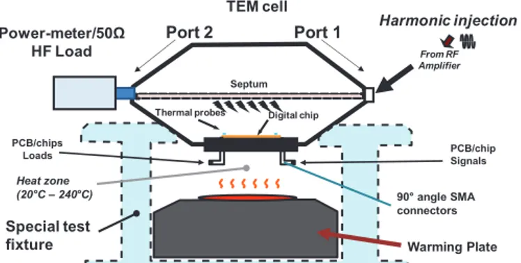
Transverse Electrical-Magnetic Cell (Crawford TEM cell) is commonly used for EMC characterization, from 1MHz up to 3GHz, at PCB and Integrated Circuits levels [8][9]. Specific PCB has to be designed to comply with the dimension of the aperture cell and the completion of shielding quality of the system. Starting from this configuration, a special fixture arm has been realized, so to maintain the PCB-TEM Cell device over the warming plate at a 4cm height to keep efficient heating action. The new constraint is to place electrical and thermal connections very close to the PCB, and with 90° angle so as to not touch the hot warming plate (Fig. 1). Acquisition of real external temperature close on board is realized by thin thermal resistor in SMD or Thin Film technology. A special attention has been made, for pertinent immunity measurements, with the thermal routing network [10]. A specific roadmap procedure and computational algorithm has been developed to drive the experiment and all the post-processing data’s.
TEM cell Power-meter/50Ω
HF Load
PCB/chips
Loads PCB/chip Signals
Heat zone (20°C – 240°C) Thermal probes 90° angle SMA connectors Digital chip Warming Plate Special test fixture From RF Amplifier Harmonic injection Port 2 Port 1 Septum
Figure 1. Schematic of Heated TEM-Cell configuration for immunity test on 10cmx10cm PCB.
2
3 Application on PWM circuit boards
3.1 First demonstrator: Integrated PWM CircuitThe first study concerns a PWM demonstrator using a Programmable IC that operates in synchronous mode, with a clock reference of 5MHz. Two inputs are used to modulate the output square signal, with an absolute cyclic rate from 5% to 94%. Main susceptibility aspects are generally, for digital mode device, the modifications of thresholds levels and switching times, due to the couplings of external parasitic signals on supply and I/O ports. Results show that mainly relative amplitude of waveform of current switching device, IVDD, has significant shifts with both harmonic frequency and
temperature aggression.
3.2 Second demonstrator: two discrete PWM circuits
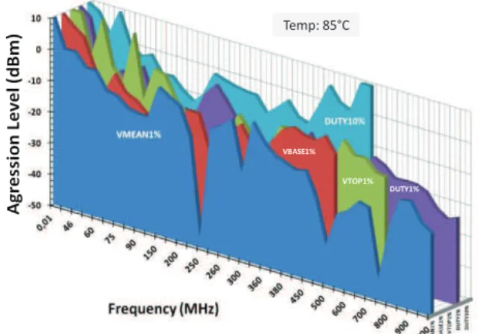
The second study concerns a dual PWM generator, dedicated for driving DC brushless motors. The PCB is compliant with TEM Cell aperture (10cm*10cm) but the area of the overall SMD circuit is about 3cm*3cm. Four main default criteria's are defined for this test the shift on duty cycle rate α, on frequency f0, on switching margins VDD
-GND, and on the mean value VMEAN. Susceptibility tests are
repeated with steps of temperature of 20°. We present main significant and pertinent results in fig.2 and fig. 3.
0 5 10 15 20 25 30 35 40 0 200 400 600 800 1000 1200 A gr e ss io n L e v e l ( d B m) Frequency (MHz) 40°C 60°C 82°C
Figure 2. Immunity table at temperature steps of 20°C for criteria "1%" on duty cycle α.
VTOP1%
DUTY1% VBASE1%
Temp: 85°C
Figure 3: 3D table representation of worst-case's immunity with PCB temperature of 85°C, for 5 criteria’s of the PWM
4 Conclusions
With these works, new modified EMC characterization approach is in progress, for real-case EMC investigations. Specific test benches have been developed based on conventional Near-Field and TEM cell immunity test setups. External aggression of light range of temperature (20°-100°) has been correctly added, so to combine both EM-Thermal effects on susceptibility of electronic chips on PCB. A focus has been made on immunity cases on PWM signals, which need to be well driven for main applications. After a measurement campaign with a wide range of different susceptibility responses of the demonstrators, main significant results are synthesized in this work. These results confirm a real significant influence of temperature on susceptibility levels of programmable or discrete chips: some critical defaults, as the shift of more than 1% of the duty cycle rate or Mean value VMEAN, are very sensitive with a non-ambient
temperature, and critical for immunity of these applications.
References
[1] J.M. Dienot, G. Lourdel, "Experimental study of thermal influence on EMC emission of digital circuit on PCB", Proceedings of the 16th International Symposium on Electromagnetic Compatibility, pp. 299-302, Zurich, February 13-18, 2005.
[2] S. Ben Dhia, E. Sicard, A. Boyer, Y. Mequignon, J.M. Dienot, " Thermal Influence on 16 bits Microcontroller Emission”, In Proc. of 2007 IEEE International Symposium on Electromagnetic Compatibility, EMC for IC session, Honolulu (USA), July 9-13, 2007.
[3] J.M. Dienot, "Characterization and simulation of digital device electromagnetic noise under non-ambient temperature conditions.", Electronics Letters Volume 43, Issue 20, pp 1073-1074, September, 2007, DOI 10.1049/el:20070495
[4] E. Hoene and al., "Simulating electromagnetic interactions in high power density converters", in Proc. of 36th IEEE Power Electronics Specialists Conference, pp. 1665-1670, Recife(BRA), 2005.
[5] S. Weber, S. Guttowski, E. Hoene, W. John and H. Reichl, " EMI Couplings from Automotive Traction Systems", In Proc. of IEEE Symposium on Electromagnetic Compatibility, Vol. 1, pp. 591-594 , Istanbul(TUR), May 11-16, 2003.
[6] D. Baudry, C. Arcambal, A. Louis, B. Mazari, and P. Eudeline, " Applications of the Near-Field Techniques in EMC Investigations", IEEE Trans. On Electromagnetic Compatibility, Vol. 49, N° 3, pp. 485-493, August 2007.
[7] K.P. Slattery, J. Neal, and W. Cui, "Near-field measurements of VLSI devices", IEEE Transactions on Electromagnetic Compatibility, vol.41, n°4, pp 374-384, November 1999.
[8] P-M. Nicolae, I-D. Nicolae, D-G. Stănescu, "Using GTEM Cells for Immunity Tests on Electronic Boards with Microcontroller", In Proc. of IEEE 2012 Symposium on EMC, pp. 44 49, Pittsburgh(USA), August 5-10, 2012
[9] X. K. Gao, E. K. Chua, and E. P. Li, “Integrated EM immunity design and diagnosis system for electronic devices”, in Proc. of 2009 International Symposium on Electromagnetic Compatibility, pp. 329-332, Kyoto, Japan, July 20-24, 2009.
[10] J.M. Dienot, E. Batista, "Real-Cases of Electromagnetic Immunity and Reliability in Embedded Electronics Architectures", in Book of Abstract of EUROEM 2012, pp 87, European Electromagnetic Symposium, Toulouse, France, 2-6 July, 2012.