HAL Id: hal-01217246
https://hal.archives-ouvertes.fr/hal-01217246
Submitted on 19 Oct 2015
HAL is a multi-disciplinary open access
archive for the deposit and dissemination of sci-entific research documents, whether they are pub-lished or not. The documents may come from teaching and research institutions in France or abroad, or from public or private research centers.
L’archive ouverte pluridisciplinaire HAL, est destinée au dépôt et à la diffusion de documents scientifiques de niveau recherche, publiés ou non, émanant des établissements d’enseignement et de recherche français ou étrangers, des laboratoires publics ou privés.
Highly reproducible, hysteresis-free, flexible strain
sensors by inkjet printing of carbon nanotubes
Fulvio Michelis, Laurence Bodelot, Yvan Bonnassieux, Bérengère Lebental
To cite this version:
Fulvio Michelis, Laurence Bodelot, Yvan Bonnassieux, Bérengère Lebental. Highly reproducible, hysteresis-free, flexible strain sensors by inkjet printing of carbon nanotubes. Carbon, Elsevier, 2015, 95, pp 1020-1026. �10.1016/j.carbon.2015.08.103�. �hal-01217246�
1
Highly reproducible, hysteresis-free, flexible strain sensors by inkjet
printing of carbon nanotubes
Fulvio Michelis1,2, Laurence Bodelot3, Yvan Bonnassieux2, Bérengère Lebental1,2*
1
Université Paris-Est, IFSTTAR, COSYS/LISIS, Paris, France
2
Laboratoire de Physique des Interfaces et Couches Minces (LPICM), UMR 7647, Ecole Polytechnique-CNRS, Palaiseau, France
3
Laboratoire de Mécanique des Solides (LMS), UMR 7649, Ecole Polytechnique-CNRS, Palaiseau, France
Abstract
In order to build upon the exceptional interest for flexible sensors based on carbon nanotube networks (CNNs), the field requires high device-to-device reproducibility. Inkjet printing has provided
outstanding results for flexible ohmic sensors in terms of reproducibility of their resistance. However, the reproducibility of the sensitivity, the most critical parameter for sensing application, has been only marginally assessed. In the present paper, CNN-based resistive strain sensors fabricated by inkjet-printing on flexible Ethylene Tetrafluoroethylene (EFTE) sheets are presented. The variability
on the device initial resistance is studied for 5 different batches of sensors from 3 to 72 devices each. The variability ranges between 8.4% and 43% depending on the size of the batches, with a 20% average. An 8-device batch with 15% variability on initial resistance is further studied for variability on the strain and thermal sensitivity. Standard deviation values are found to be as low as 16% on the strain sensitivity and 8% on the temperature sensitivity. Moreover, the devices are hysteresis free, a
rare achievement for CNT strain sensors on plastics.
1.
Introduction
Owing to their very large specific surface area [1], carbon nanotubes (CNTs) have been of utmost interest for sensing applications since the early days of CNT research [2]. Ohmic or transistor devices
using CNTs deposited or grown on rigid substrates have demonstrated exceptional sensitivity to their
environment, leading to various examples of analytical (humidity, pH, gas, chemical or biological species) [3], mechanical (strain, pressure) [4] or radiation (thermal or infrared, UV) [5] sensors. Following the quick rise of CNT-based flexible electronics [6], a wide range of flexible CNT sensors was proposed [7], with the goal of providing the next generation of wearable devices [8] for human
welfare monitoring or wireless sensor networks [9] for infrastructure [10] or environmental
*
2 monitoring [11]. With their mechanical robustness (high Young’s modulus, low bending rigidity, low buckling properties, high tensile strength [2] [12]) flexible CNT sensors are expected to provide long-lasting, reliable devices compatible with industrial requirements.
The active component of these sensors most often consists of wet-processed carbon nanotube
networks (CNNs) [13]. CNNs are films of randomly or partially organized CNTs and their thickness ranges from a few tens of nanometers to a few tens of micrometers. Their fabrication methods include filtration and extraction of buckypaper [14], spray coating [15], layer-by-layer assembly [10] as well as contact (roll-to-roll [16] or transfer-based [17]) and non-contact (aerosol [18] or inkjet [19])
printing techniques. Except for the buckypaper approach, all these methods rely on deposition over a substrate. Studies have yielded strain gauges [18] [20], gas sensors [21], photodetectors [22] and chemistors [23]. Table 1 in Supplementary information 1 provides an extensive study of the state of the art of CNN rigid and flexible sensors.
A long-standing, acute challenge for industrial applications of flexible CNN sensors lies in their low
device-to-device reproducibility [24]. Reproducibility specifically addresses two factors, firstly, the standard deviation in initial device resistance, secondly, the standard deviation in device sensitivity. Device-to-device variability has been discussed repeatedly with regard to CNN-based flexible resistors [18] and transistors [25] and various causes have been reported, including liquid-phase dispersion issues of CNTs [26], variability in CNT properties within a batch (semiconducting versus
metallic, diameter, length, sidewall defects) [24], quality of the CNT-to-electrode contacts or surface roughness of the flexible substrates [13].
In spite of this, reports on CNN sensors (either rigid of flexible) rarely provide standard deviation on the resistance level (see Table 1, SI1). Lowest reported standard deviations have been achieved via
inkjet-printing: Benchirouf et al. [27] reports 3.5% standard deviation on the resistance level of 3-device-batches (strain sensors) while Lesch et al. [19] reports 7% and 20% standard deviation on the two fitting parameters of the amperometric cycle of antioxidant power sensors, for a 6-device batch.
Regarding to studying variability on sensitivity, Lesch et al. [27] and Karimov et al [28] provide the response of respectively 2 sets and 1 set of 2 devices. Kim et al. [29] , Mirica et al [30], Takeo et al
[30] compare respectively 4, 3 and 3 sensors from the same batch, but provide no standard deviation on the sensitivity. Beyond this, Li et al. [31] provide the standard deviation on the benchmarking parameters (slope/sensitivity and Y-intercept, respectively 7% and 25%) of a 3-device batch of gas sensors on SiO2. Finally, the most statistically relevant results stem from Lee et al. [32]. Lee et al. provide the full dispersion plot of the sensitivity of a batch of 21 sensors on SiO2, which spans two
3 In the present paper, we provide a detailed study on resistance and sensitivity variability in batch-fabricated inkjet-printed CNN-based flexible sensors. The study focuses on strain sensors based on multi-walled CNTs (MWCNTs) printed on Ethylene Tetrafluoroethylene (EFTE) sheets. After
describing the fabrication process, we prove the high device-to-device reproducibility in terms of strain and temperature sensitivity. We also present the sensing performance, including exceptional cyclability and hysteresis-free operation.
2.
Methods
2.1MaterialsMWCNTs Graphistrenth C100 are purchased from Arkema. The solvents 1,2–Dichlorobenzene
(Dichlorobenzene hereafter), Acetone and Methanol and the surfactant Sodium Dodecyl Benzene Sulphonate (SDBS) are purchased from Sigma-Aldrich. The substrate is a 0.125 mm thick, 30 cm by 30 cm foil of Ethylene Tetrafluoroethylene (ETFE) with 90 nm roughness (calculated as in [33], see formula in Supplementary Information (SI) 1) supplied by Goodfellow.
2.2Carbon nanotube ink preparation
The MWCNTs are dispersed in dichlorobenzene at 0.02 wt.% using an ultrasonic probe (Bioblock Scientific VibraCell 75043) operated at 150 W for 20 min followed by centrifugation at 10 kG for 4 h. In order to increase ink-wettability on ETFE and improve homogeneity of the deposition, SDBS at 0.3 wt.% is added to the supernatant using a 20 min sonication bath (see details in SI2) [13]. The
resulting dispersion, called ink in the rest of the paper, is stable for over 3 months.
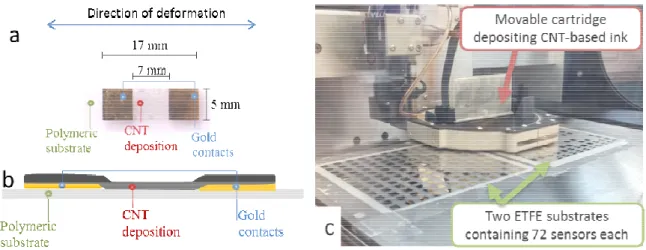
2.3Device fabrication
The device structure is shown in Figure 1a and b. The ETFE foils are first cleaned with acetone and dried under nitrogen flow. Pairs of 100 nm thin, 5 mm x 5 mm gold electrodes spaced by 7 mm are deposited using thermal evaporation under vacuum (10-7 mbar). The MWCNTs are then deposited by inkjet printing using the customizable Dimatix Material Inkjet Printer 2800 with DMP-11601
cartridges. The cartridge is kept at room temperature during printing and the substrate is heated to 55 °C. The printing pattern is a 17 mm x 5 mm rectangle positioned to fully cover both electrodes of each device, in order to ensure proper electrical contact. Several layers can be printed successively depending on the properties targeted for the devices. Residual dichlorobenzene and surfactant are rinsed away by immersion and slight agitation in methanol and acetone for 8s each, followed by
drying under nitrogen flow.
The number of layers and the rinsing periodicity strongly impact the final device resistance (see details in SI.3). We optimized these parameters in order to reach device resistances below 1 MΩ
(threshold value required for compatibility with while keeping the fabrication time
printed layers rinsed every two layers.
ETFE foils (Figure 1c). The time required for the production of rinsing every 2 layers is 3 and 5 days
Figure 1 a) Image of a CNT-based devic b) Cross-sectional diagram of the device substrate contains 72 sensors.
2.4Physical and electrical
The devices are observed via optical
deposition thickness is measured electrical contacting is achieved The resistance is measured in a
Keithley 2612 source measurement unit imposes a constant, continuous current i (from 4 to 7 μA) while a National Instrument NI9212 acquisition card
a frequency of 6.7 Hz. All electrical characterizations are performed within a electromagnetic shielding.
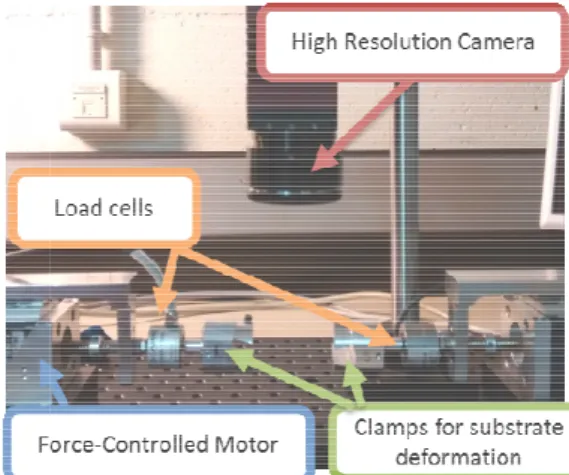
2.5Strain sensing
To characterize the devices as strain gauges, longitudinal deformation to the substrate Deformations are applied by gluing
force-controlled motors (Figure
ALF328 load cells. A CCD camera is used to
required for compatibility with commercial acquisition cards; see
the fabrication time manageable. Devices presented here are obtained from 20 printed layers rinsed every two layers. They are produced by batches of either 8 or 144
he time required for the production of 8 or 144 devices 5 days respectively.
device printed on ETFE (top view) with device size and direction of deformation diagram of the device. c) Ink-jet printing of a 144-device batch on
side-lectrical characterizations
ia optical and scanning electron microscopy SEM (
measured via profilometry (Dektak 150). For resistance measurements, by gluing thin copper wires to the gold electrodes with silver paste. The resistance is measured in a 4-probe configuration to limit the impact of contact resistances: a Keithley 2612 source measurement unit imposes a constant, continuous current i
μA) while a National Instrument NI9212 acquisition card measures the output voltage at
a frequency of 6.7 Hz. All electrical characterizations are performed within a Faraday cage
To characterize the devices as strain gauges, variations in resistance are measured deformation to the substrate (deformations applied along the main axis
by gluing the two opposite sides of a substrate to two clamps mounted on
Figure 2). Forces up to 8N are applied. The force is measured using . A CCD camera is used to determine the resulting deformation
4 ; see next section 2.4) Devices presented here are obtained from 20 either 8 or 144 sensors on
144 devices with 20 layers and
with device size and direction of deformation. -by-side ETFE foils. Each
(Hitachi S 4800). The
For resistance measurements, wires to the gold electrodes with silver paste. probe configuration to limit the impact of contact resistances: a Keithley 2612 source measurement unit imposes a constant, continuous current in the µA range measures the output voltage at
Faraday cage providing
measured while applying main axis, see Figure 1a). substrate to two clamps mounted on
. The force is measured using Althen of the substrate: the
displacement of surface patterns
levels reach up to 2500 με. Devices are characterized either
characterization of the piezoresistive response
a thermocouple.
2.6Temperature sensitivity
The temperature sensitivity of the resistance is also
controlled by the Thermoelectric Temperature Controller LFI 3751 by Wavelength Electronics. The resistance is measured with a Keithl
characterization, the samples are positioned
ensure that relative humidity remain
Figure 2 Extensometric bench used for
3.
Results and interpretation
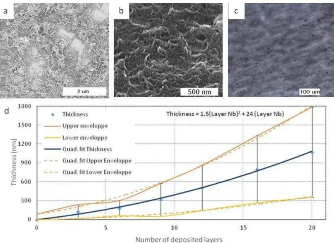
3.1Morphology of the carbon nanotube network
SEM images of a single layer deposition (
randomly on the surface, with a surface density of high resolution images (see SI
probably due to loss of material during rinsing homogeneity of the deposition improves and t surface is entirely covered (Figure
Up to 20 layers, the thickness of the deposition increases
reaches 1100 nm for a 20-layer deposition surface is very rough. The roughness
displacement of surface patterns is tracked during deformation and then converted into
either separately or by series of 4 sensors on the same substrate.
of the piezoresistive response, the temperature is not controlled but is monitored by
Temperature sensitivity
The temperature sensitivity of the resistance is also measured. The devices are placed on a hot plate trolled by the Thermoelectric Temperature Controller LFI 3751 by Wavelength Electronics. The resistance is measured with a Keithley S4200 using a 4-probe configuration. During temperature characterization, the samples are positioned in a shielded environment under nitrogen flow to
remains constant at 0.8 % during the duration of the measurement.
Extensometric bench used for electromechanical characterization
and interpretation
of the carbon nanotube network
deposition (Figure 3a) show that CNTs overlap each over and
, with a surface density of 240 CNT/µm² as obtained by
I5 for more details). Numerous micrometric holes are observed, loss of material during rinsing. When increasing the number of
homogeneity of the deposition improves and the surface coverage increases. At 20 depositions, the Figure 3b and c).
he thickness of the deposition increases quadratically for each additional
layer deposition (Figure 3d). As expected from the SEM images, the roughness (error bars in Figure 3d) increases with the number of layers
5 and then converted into strain. Strain
separately or by series of 4 sensors on the same substrate. During , the temperature is not controlled but is monitored by
vices are placed on a hot plate trolled by the Thermoelectric Temperature Controller LFI 3751 by Wavelength Electronics. The probe configuration. During temperature nt under nitrogen flow to
duration of the measurement.
characterization.
overlap each over and are spread
as obtained by visual counting on Numerous micrometric holes are observed, When increasing the number of layers, the he surface coverage increases. At 20 depositions, the
for each additional layer and
As expected from the SEM images, the film increases with the number of layers,
6 from 110 nm for 3 layers up to 720 nm for 20 layers. The substrate itself contributes to the overall roughness by only 90 nm. The faster than linear rise of the thickness (clear despite the large roughness/error bars) suggests that the film porosity increases with increasing number of layers,
probably due to the imperfect filling of the holes (Figure 3a).
Figure 3 a) SEM image of 1-layer deposition. Micrometric holes are observed in the layer; they are attributed to loss of matter during rinsing. b) SEM image of 20-layer deposition. A uniform coverage can be observed. c) Optical microscopy image of a 20-layer deposition, showing homogeneity and uniformity at a micro scale. d) Thickness of the deposition with respect to number of layers. The rise is roughly quadratic. The error bars represent the surface roughness (the error bar for 0 layer is the roughness of the substrate, 90nm). They are used to define the envelope of the thickness curve. Both upper and lower envelopes also rise quadratically.
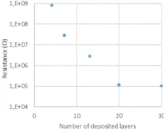
3.2Device resistance
A single layer has a resistance in the GΩ range, too high for sensing applications. As expected, the resistance decreases as the number of layers increases, in accordance with the literature on CNTs
percolated networks [34]. It reaches the 1 MΩ range at 15 layers, the 150 kΩ range at 20 layers and the 100 kΩ range at 30 layers (Figure 4). The lowest resistance reached is 104 kΩ (87 kΩ/sq) for a 30-layer deposition. This range of magnitude of resistance, though quite high compared to CNN-based inkjet-printed flexible transparent conducting layers [35], is fully compatible with sensing
applications. The decrease of resistance as a function of the thickness is much faster than for homogeneous thin films (see for instance Fuchs model
roughness-to-thickness ratio of the film
model for rough thin films [37]).
Standard deviations for 3- to 72 (3 devics) to 43 % (72 devices) different batches are provided in SI6 to a degraded homogeneity in the gold
batches (3 to 8 devices; standard are attributed to slight variations
In the rest of the paper, we discuss a 20 15 % (23 kΩ) standard deviation.
and was of sufficient size for further sensitivity analysis.
had only 3 devices and thus appeared too small for standard deviation calculation
Figure 4 Resistance of the deposition with respect to number of layers.
3.3Reproducibility of strain sensing performances
As expected from the literature on varies when they are subjected to
strain, the strain-stress relationship of the
properties of the film). For large strains
the device initial length L by ∆L=10
to 0.6 % (about 900 Ω) of the initial resistance
resistance variation measured on the gold electrodes when they are subjected to strain
The decrease of resistance as a function of the thickness is much faster than for for instance Fuchs model [36]). It is attributed to
thickness ratio of the films when the number of layer increases (as predicted by Namba
72-device-batches of 20-layer devices were found to
(72 devices) with an average at 20%. (Details on the standard deviations of the different batches are provided in SI6). The larger standard deviation for the large batc
eity in the gold deposition over the full area of the ETF
d deviations ranging from 8.4% to 18%), the diff s in the ink quality.
discuss a 20-layer, 8-sensor batch with average resistance 156
) standard deviation. This batch was selected as it featured the lowest average resistance size for further sensitivity analysis. The batch with lowest standard deviation
appeared too small for standard deviation calculation
stance of the deposition with respect to number of layers.
Reproducibility of strain sensing performances
As expected from the literature on CNNs strain sensitivity [15] [18], the resistance subjected to longitudinal strains of up to 2500 µε (Figure 1
stress relationship of the substrate is linear (see SI7 for details on the mechanical
For large strains up to 2500 με (1 με strain corresponds to an extension
L=10-6L), the resistance increases quadratically with strain
) of the initial resistance (Figure 5a), in accordance with
resistance variation measured on the gold electrodes when they are subjected to strain
7 The decrease of resistance as a function of the thickness is much faster than for ). It is attributed to the decrease of the s when the number of layer increases (as predicted by Namba
found to range from 8.4 % (Details on the standard deviations of the The larger standard deviation for the large batch is attributed FE sheet. For smaller
ferences in variability
e resistance 156 kΩ and the lowest average resistance The batch with lowest standard deviation
appeared too small for standard deviation calculation.
resistance of the devices Figure 1a). In this range of for details on the mechanical
με strain corresponds to an extension ∆L of L), the resistance increases quadratically with strain, reaching up
), in accordance with [38] (see SI 8). The resistance variation measured on the gold electrodes when they are subjected to strain of up to
8 2500 µε is 10 Ω, over 10 times smaller than the resistance variation for the whole sensing element. Consequently, we can deduce that the piezoresistive effect is not due to the electrodes only.
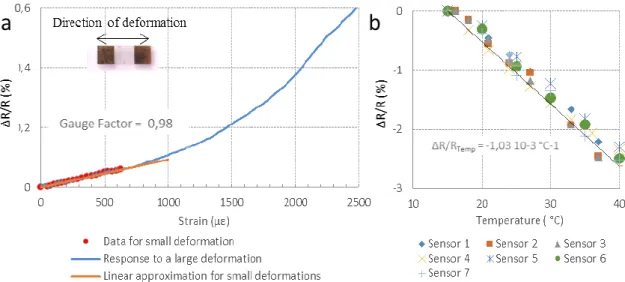
All devices feature a linear behavior in the small strain regime. The linear range exceeds 400 µε for all the devices. 75 % have a linear range of over 600 µε and 50 % above 800 µε. The strain sensitivity,
also called gauge factor (GF), is defined as the slope of ∆R/R vs ε curve in the linear regime. It is found to be 0.90 ± 0.14 for an 8-device batch, corresponding to 16% standard deviation on the GF. The 0.9 GF value is the only reported GF for printed CNT resistive strain sensors [39]. This is the first
quantitative evaluation of the variability in sensitivity for batch-produced CNT-based flexible sensors.
This GF value is comparable to the GF of commercially available strain gauges (between 1 and 2), though the standard deviation on the resistance and on the gauge factor are still higher than the dispersion reported in the datasheets of commercial devices (respectively 2% and 5% standard deviation on the resistance and on the GF) [40] [41]. Much higher GF values can be achieved in devices with oriented CNT [8] or closer to the CNN’s percolation threshold, including
buckypaper-based devices (for instance [42]). However operation close to the percolation threshold has a detrimental impact on device-to-device reproducibility [18].
3.4Reproducibility of temperature sensitivity
Temperature is known to strongly influence both the conductivity of CNNs [43] and the mechanical response of polymer foils [44]. Hence, we studied the dependence of the devices on temperature (Figure 5b). The results show that the resistance decreases linearly with temperature, in accordance
with other studies [43] [45]. The temperature sensitivity, defined as the slope of the ∆R/R versus temperature curve, is equal to -1.0x10⁻³ K-1. This coefficient is comparable to those published in [43]and [46] for CNT devices fabricated respectively on silicon and PET. The thermal sensitivity cannot be explained by the thermal expansion of the substrate (0.9-1.7x10⁻⁴K-1) [47]), as the effect would be a positive thermal sensitivity in the range of +0.8-1.5x10⁻⁴ K-1. Dehghani et al. [43] proposes
that the thermal sensitivity is mostly due to thermal variation in the CNT resistivity.
The standard deviation in the temperature sensitivity is as low as 8 % over 7 devices, even lower than the standard deviation over resistance (15%) and over gauge factor (16%). The possibility of compensating for temperature is critical for future applications of this strain gauge.
Figure 5 a) Resistance variation with respect to strain. The linear regime reaches up to 7 factor of the device presented here is 0,98
dependence of resistance on temperature.
3.5Response time
We assessed the device response time
once the target strain is reached
target (see Figure 6a). The response time regime of the device). This suggests that th
static applications (frequencies well below
As expected, out of the linear range, the response
response time is as high as 19 s; it appears that from about 1200 µε, the device cannot follow the increase in strain, thus suggesting
Figure 6 Measurement of device response time
variation with respect to strain. The linear regime reaches up to 700 με for this device is 0,98. Overall, the response up to large strains is roughly quadratic. on temperature. The temperature sensitivity is equal to -1.0x10⁻³ K-1.
We assessed the device response time, defined here as the time to reach 95 % of the expected value
once the target strain is reached (Figure 6a and b). The strain is increased linearly over 5 The response time was found to be 3.6 s for a 500 µε strain
This suggests that the devices should preferably be used for static
(frequencies well below 0.3 Hz/period well over 3.6 s).
ut of the linear range, the response time is much higher. For a 1600 µε
s; it appears that from about 1200 µε, the device cannot follow the increase in strain, thus suggesting a settling effect in the CNN at larger strain levels
esponse time: a) 3.6 s under small strains (500 µε). b) 19 s under large strains
9
for this device. The gauge is roughly quadratic.b) Linear
% of the expected value
The strain is increased linearly over 5 s to reach its strain (within the linear be used for static or
quasi-a 1600 µε strquasi-ain, the s; it appears that from about 1200 µε, the device cannot follow the
in the CNN at larger strain levels.
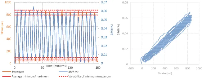
3.6Quasi-static cyclability and hysteresis
We evaluated the quasi-static submitted to cyclic loadings (20
periodicity (2 mHz, well below the frequency
response is acquired at 6.7 Hz (3600
Over 3 hours and 20 cycles, the devices display remarkable (Figure 7a and b). The discrepancy between
measured during unloading is only devices compared to the state of the art
significant a baseline drift, though there
(Figure 7b). The standard deviation over the maximum resistance value (0 cycles (range 0.55-0.61x10⁻²). Based on the thermal sensitivity of the devices ( resistance variation of 6x10⁻⁴ can be explained by only 0.6°C of thermal variatio
magnitude of temperature variations (between 0.3°C and 1°C) measured in the climate
room where the experiments were carried out. Hence, the variability in the resistance/strain curves is attributed to temperature variatio
Hysteresis free operation is possible stress curves are provided in SI9
the devices clearly display hysteresis and creep effects. The creep effect on the resistance can be attributed to the creep of the substrate, estimated at 27
periodicity.
Figure 7 a) Response of a device to 20 cycles of strains between 0 and 800 observed. b) Corresponding resistance
yclability and hysteresis-free operation in quasi-static mode
static cyclability of the devices in the linear regime 20 cycles over 3 hours) in the linear regime (800
well below the frequency limit defined using the response time).
(3600 measurements per period).
the devices display remarkable cyclability and hysteresis he discrepancy between gauge factor measured during loading
only 2.7 % (figure 7a), which underlines the hig
ate of the art [48] [49]. As can be observed in Figure 7a, there is no
though there is a significant variability in the cycle min and max values deviation over the maximum resistance value (0.58x10
). Based on the thermal sensitivity of the devices (
can be explained by only 0.6°C of thermal variation. This is the range of magnitude of temperature variations (between 0.3°C and 1°C) measured in the climate
room where the experiments were carried out. Hence, the variability in the resistance/strain curves is attributed to temperature variations.
Hysteresis free operation is possible only in the linear regime of the devices. Additional resistance 9 for strains up to 2500µε and up to 4000µε. In
he devices clearly display hysteresis and creep effects. The creep effect on the resistance can be attributed to the creep of the substrate, estimated at 27µε by cycle for 8N load cycles
of a device to 20 cycles of strains between 0 and 800 με. No evident hysteresis or baseline drift is resistance-strain plot. The extent of the bundle of resistance-strain curve is due to a slight
10
static mode
in the linear regime. The devices are ) in the linear regime (800 με) with 9 minutes defined using the response time). The device
cyclability and hysteresis-free operation loading and the one , which underlines the high reversibility of the As can be observed in Figure 7a, there is no
variability in the cycle min and max values 58x10-2) is 4.7% over 20 ). Based on the thermal sensitivity of the devices (-1.0x10⁻³), a relative n. This is the range of magnitude of temperature variations (between 0.3°C and 1°C) measured in the climate-controlled
room where the experiments were carried out. Hence, the variability in the resistance/strain curves
in the linear regime of the devices. Additional resistance-n this raresistance-nge of strairesistance-n,
he devices clearly display hysteresis and creep effects. The creep effect on the resistance can be by cycle for 8N load cycles with 5 min
No evident hysteresis or baseline drift is strain curve is due to a slight
11
variability (4.7%) in min and max resistance value. It is attributed to temperature variations in the range of approx. ±0.3 °C.
4.
Conclusions
In this paper, we study for the first time the sensitivity variability of CNN-based flexible ohmic sensors. We focus on CNN-based strain gauges on Ethylene Tetrafluoroethylene sheets achieved by
inkjet printing of MWCNTs dispersed in Dichlorobenzene with SDBS as a surfactant. The use of inkjet printing produces highly reproducible devices with low variability in resistance (best standard deviation 8.4 % for a 3-device batch; 20% standard deviation averagely between 5 batches between 3 and 72 devices), gauge factor (16 % standard deviation for a 8-device batch with 15% standard deviation on the resistance), and temperature sensitivity (8 % standard deviation for a 8-device batch
with 15% standard deviation on the resistance). Compared to the state of the art of CNN strain gauges, the devices demonstrate remarkable cyclability and hysteresis-free operation. These results open the road towards the use of the proposed sensors in real-life applications.
5.
Acknowledgments
The authors acknowledge support from ANR (France) for project Sense-City (ANR-10-EQPX-48). The authors also thank Costel –Sorin Cojocaru, Denis Tondelier, Eléonor Caristan and Jean-Luc Sorin from LPICM and IFSTTAR laboratories for their help and support.
Bibliography
[1] A. Peigney, C. Laurent, E. Flahaut, R. Bacsa and A. Rousset, "Specific surface area of carbon nanotubes and bundles of carbon nanotubes," Carbon, vol. 39, no. 4, pp. 507-514, 2001.
[2] R. H. Baughman, A. A. Zakhidov and W. A. d. Heer, "Carbon Nanotubes—the Route Toward Applications," Science, vol. 297, p. 787, 2002.
[3] J. Kong, N. R. Franklin, C. Zhou, M. G. Chapline, S. Peng, K. Cho and H. Dai, "Nanotube Molecular Wires as Chemical Sensors," Science, vol. 287, p. 622, 2000.
[4] Y. Li, Y. Zhao, Y. Zhu, J. Rodriguez, J. Morante, E. Mendozac, C. Poa and S. Silva, "Mechanical and NH3 sensing properties of long multi-walled carbon nanotube ropes," Carbon, vol. 44, no. 9, pp. 1821-1825, 2006.
[5] P. W. Barone, S. B. D. A. Heller and M. S. Strano, "Near-infrared optical sensors based on single-walled carbon nanotubes," Nature Materials , vol. 4, pp. 86-92, 2005.
[6] K. Bradley, J.-C. P. Gabriel and G. Grüner, "Flexible Nanotube Electronics," Nano Letters, vol. 3, no. 10, pp. 1353-1355, 2003.
12 [7] M. Mabrook, C. Pearson, A. Jombert, D. Zeze and M. Petty, "The morphology, electrical conductivity and vapour sensing ability of inkjet-printed thin films of single-wall carbon nanotubes," Carbon, vol. 47, no. 3, pp. 752-757, 2009.
[8] T. Yamada, Y. Hayamizu, Y. Yamamoto, Y. Yomogida, A. Izadi-Najafabadi, D. N. Futaba and K. Hata, "A stretchable carbon nanotube strain sensor for human-motion detection," Nature
Nanotechnology, vol. 6, pp. 296-301, 2011.
[9] S. Laflamme, M. Kollosche, J. Connor and G. Kofod, "Robust Flexible Capacitive Surface Sensor for Structural Health Monitoring Applications," Journal of Engineering Mechanics, vol. 139, no. 7, pp. 879-885, 2013.
[10] K. J. Loh, J. Kim, J. P. Lynch, N. W. S. Kam and N. A. Kotov, "Multifunctional layer-by-layer carbon nanotube–polyelectrolyte thin films for strain and corrosion sensing," Smart Materials and
Structures, vol. 16, pp. 429-438, 2007.
[11] M. S. Mauter and M. Elimelech, "Environmental Applications of Carbon-Based Nanomaterials,"
Environmental Science and Technology, vol. 42, no. 16, pp. 5843-5859, 2008.
[12] M.-F. Yu, O. Lourie, M. J. Dyer and K. Moloni, "Strength and Breaking Mechanism of Multiwalled Carbon Nanotubes Under Tensile Load," Science, vol. 287, p. 637, 2000.
[13] A. Saha, C. Jiang and A. A. Martí, "Carbon nanotube networks on different platforms," Carbon, vol. 79, pp. 1-18, 2014.
[14] Y. Li and M. Kröger, "A theoretical evaluation of the effects of carbon nanotube entanglement and bundling on the structural and mechanical properties of buckypaper," Carbon, vol. 50, no. 5, pp. 1793-1806, 2012.
[15] D. J. Lipomi, M. Vosgueritchian, B. C.-K. Tee, S. L. Hellstrom, J. A. Lee, C. H. Fox and Z. Bao, "Skin-like pressure and strain sensors based on transparent elastic films of carbon nanotubes," Nature
Nanotechnology, vol. 6, pp. 788-792, 2011.
[16] J. Noh, M. Jung, K. Jung, G. Lee, S. Lim, D. Kim, S. Kim, J. M. Tour and G. Cho, "Integrable single walled carbon nanotube (SWNT) network based thin film transistors using roll-to-roll gravure and inkjet," Organic Electronics, vol. 12, no. 12, pp. 2185-2191, 2011.
[17] P. H. Lau, K. Takei, C. Wang, Y. Ju, J. Kim, Z. Yu, T. Takahashi, G. Cho and A. Javey, "Fully Printed, High Performance Carbon Nanotube Thin-Film Transistors on Flexible Substrates," Nano Letters, vol. 13, no. 8, pp. 3864-3869, 2013.
[18] S. Li, J. G. Park, S. Wang, R. Liang, C. Zhang and B. Wang, "Working mechanisms of strain sensors utilizing aligned carbon nanotube network and aerosol jet printed electrodes," Carbon, vol. 73, pp. 303-309, 2014.
[19] A. Lesch, F. Cortés-Salazar, M. Prudent, J. Delobel, S. Rastgar, N. Lion, J.-D. Tissot, P. Tacchini and H. H. Girault, "Large scale inkjet-printing of carbon nanotubes electrodes for antioxidant assays in blood bags," Journal of Electroanalytical Chemisty, Vols. 717-718, pp. 61-68, 2014.
[20] D. J. Cohen, D. Mitra, K. Peterson and M. M. Maharbiz, "A Highly Elastic, Capacitive Strain Gauge Based on Percolating Nanotube Networks," Nano Letters, vol. 12, pp. 1821-1825, 2012.
13 [21] F. Rigoni, G. Drera, S. Pagliara and A. Goldoni, "High sensitivity, moisture selective, ammonia gas sensors based on single-walled carbon nanotubes functionalized with indium tin oxide nanoparticles," Carbon, vol. 80, pp. 356-363, 2014.
[22] A. Gohier, A. Dhar, L. Gorintin, P. Bondavalli, Y. Bonnassieux and C. S. Cojocaru, "All-printed infrared sensor based on multiwalled carbon nanotubes," Applied Physics Letters, vol. 98, p. 063103, 2011.
[23] J. M. A. Katherine A. Mirica, J. G. Weis, J. M. Schnorr and T. M. Swager, "Rapid prototyping of carbon-based chemiresistive gas sensors on paper," PNAS, pp. 3265-3270, 2013.
[24] B. Y. Lee, M. G. Sung, J. Lee, K. Y. Baik, Y.-K. Kwon, M.-S. Lee and S. Hong, "Universal Parameters for Carbon Nanotube Network-Based Sensors: Can Nanotube Sensors Be Reproducible?," ACS
Nano, vol. 5, no. 6, pp. 4373-4379, 2011.
[25] C. Wang, J.-C. Chien, K. Takei, T. Takahashi and J. Nah, "Extremely Bendable, High-Performance Integrated Circuits Using Semiconducting Carbon Nanotube Networks for Digital, Analog, and Radio-Frequency Applications," Nano Letters, vol. 12, pp. 1527-1533, 2012.
[26] S. Kim, T. Kim, Y. Kim, H. Choi, H. Lim, S. Yang and C. Park, "Surface modifications for the effective dispersion of carbon nanotubes in solvents and polymers," Carbon, vol. 50, no. 1, pp. 3-33, 2012.
[27] A. Benchirouf, E. Sowade, A. Al-Hamry, T. Blaudeck, O. Kanoun and R. Baumann, "Investigation of RFID passive strain sensors based on carbon nanotubes using inkjet printing technology," in
9th IEEE Int. Multiconference on Systems, Signals and Devices, 2012.
[28] K. S. Karimov, F. A. Khalid and M. T. S. Chani, "Carbon nanotubes based strain sensors,"
Measurement, vol. 45, pp. 918-921, 2012.
[29] J. Kim, J.-H. Yun, J.-W. Song and C.-S. Han, "The spontaneous metal-sitting structure on carbon nanotube arrays positioned by inkjet printing for wafer-scale production of high sensitive gas sensor units," Sensors and Actuators B: Chemical, vol. 135, pp. 587-591, 2009.
[30] K. A. Mirica, J. M. Azzarelli, J. G. Weis, J. M. Schnorr and T. M. Swager, "Rapid prototyping of carbon-based chemiresistive gas sensors on paper," PNAS, pp. 3265-3270, 2013.
[31] J. Li, Y. Lu, Q. Ye, M. Cinke, J. Han and M. Meyyappan, "Carbon Nanotube Sensors for Gas and Organic Vapor Detection," Nano Letters, vol. 3, pp. 929-933, 2003.
[32] B. Y. Lee, M. G. Sung, J. Lee, K. Y. Baik, Y.-K. Kwon, M.-S. Lee and S. Hong, "Universal Parameters for Carbon Nanotube Network-Based Sensors: Can Nanotube Sensors Be Reproducible?," ACS
Nano, vol. 5, pp. 4373-4379, 2011.
[33] E. P. DeGarmo, J. T. Black and R. A. Kohser, Materials and Processes in Manufacturing, Wiley, 2003.
[34] P. Slobodian, P. Riha, A. Lengalova, R. Olejnik and D. Kimmer, "Effect of compressive strain on electric resistance of multi-wall carbon nanotube networks," Journal of Experimental
14 [35] O.-S. Kwon, H. Kim, H. Ko, J. Lee, B. Lee and C.-H. Jung, "Fabrication and characterization of inkjet-printed carbon nanotube electrode patterns on paper," Carbon, vol. 58, pp. 116-127, 2013.
[36] A. A. Cottey, "The electrical conductivity of thin metal films with very smooth surfaces," Thin
Solid Films, vol. 1, no. 4, p. 297–307, 1938.
[37] H. Hoffmann and J. Vancea, "Critical assessment of thickness-dependent conductivity of thin metal films," Thin Solid Films, vol. 85, no. 2, p. 147–167, 1981.
[38] F. J. Baeza, O. Galao, E. Zornoza and E. Garcés, "Multifunctional Cement Composites Strain and Damage Sensors Applied on Reinforced Concrete Structural Elements," Materials, vol. 6, pp. 841-855, 2013.
[39] T. Kim, J. Byun, H. Song and Y. Hong, "Inkjet-printed SWCNT films for stretchable electrode and strain sensor applications," in Device Research Conference, 2012.
[40] E. Omega, "Strain gauge technical data sheet".
[41] l. Tokyo Sokki Kenkyujo Co., "Strain Gauge Performance Characteristics," 2011.
[42] N. Hu, Y. Karube, M. Arai, T. Watanabe and C. Yan, "Investigation on sensitivity of a polymer/carbon nanotube composite strain sensor," Carbon , vol. 48, pp. 680-687, 2010.
[43] S. Dehghani, M. K. Moravvej-Farshi and M. H. Sheikhi, "Temperature Dependence of Electrical Resistance of Individual Carbon Nanotubes and Carbon Nanotubes Network," Modern Physics
Letters B, vol. 26, no. 21, 2012.
[44] Fisher | Moore, "Ethylene tetrafluoroethylene (ETFE) Technical Information," 1999.
[45] W. S. Bao, S. A. Meguid, Z. Z. H. and G. Zeng, "Tunneling resistance and its effect on the electrical conductivity of carbon nanotube nanocomposites," Journal of Applied Physics, vol. 111, no. 093726, 2012.
[46] V. Scardaci, R. Coull, J. Coleman, L. Byrne and G. Scott, "Carbon Nanotube network based sensors," in Conference on Nanotechnology IEEE-Nano, Birmingham, 2012.
[47] "Copolymère d'Ethylène-tetrafluoroéthylène (ETFE) - Informations Matériau," [Online]. Available: http://www.goodfellow.com/F/Copolymere-d'Ethylene-tetrafluoroethylene.html.
[48] R. Zhang, H. Deng, R. Valenca, J. Jin, Q. Fu, E. Bilotti and T. Peijs, "Strain sensing behaviour of elastomeric composite films containing carbon nanotubes under cyclic loading," Composites
Science and Technology, vol. 74, no. 24, pp. 1-5, 2013.
[49] R. K. Srivastava, V. S. M. Vemuru, Y. Zeng, R. Vajtai, S. Nagarajaiah, P. M. Ajayan and A. Srivastava, "The strain sensing and thermal–mechanical behavior of flexible multi-walled carbon nanotube/polystyrene composite films," Carbon, vol. 49, no. 12, pp. 3928-3936, 2011.
[50] A. Benchirouf, E. Sowade, A. Al-Hamry, T. Blaudeck, O. Kanoun and R. Baumann, "Investigation of RFID passive strain sensors based on carbon nanotubes using inkjet printing technology," in