HAL Id: hal-01302652
https://hal.inria.fr/hal-01302652
Submitted on 14 Apr 2016
HAL is a multi-disciplinary open access
archive for the deposit and dissemination of
sci-entific research documents, whether they are
pub-lished or not. The documents may come from
teaching and research institutions in France or
abroad, or from public or private research centers.
L’archive ouverte pluridisciplinaire HAL, est
destinée au dépôt et à la diffusion de documents
scientifiques de niveau recherche, publiés ou non,
émanant des établissements d’enseignement et de
recherche français ou étrangers, des laboratoires
publics ou privés.
On the FPGA-based implementation of a flexible
waveform from a high-level description: Application to
LTE FFT case study
Mai-Thanh Tran, Matthieu Gautier, Emmanuel Casseau
To cite this version:
Mai-Thanh Tran, Matthieu Gautier, Emmanuel Casseau. On the FPGA-based implementation of a
flexible waveform from a high-level description: Application to LTE FFT case study. EAI International
Conference on Cognitive Radio Oriented Wireless Networks (Crowncom16), May 2016, Grenoble,
France. �hal-01302652�
flexible waveform from a high-level description:
Application to LTE FFT case study
Mai-Thanh Tran, Matthieu Gautier, and Emmanuel Casseau
University of Rennes 1, IRISA, France,
{mai-thanh.tran,matthieu.gautier,emmanuel.casseau}@irisa.fr
Abstract. The Field Programmable Gate Array (FPGA) technology is expected to play a key role in the development of Software Defined Radio (SDR) platforms. To this aim, leveraging the nascent High-Level Synthesis (HLS) tools, a design flow from high-level specifications to Register-Transfer Level (RTL) description can be thought to generate processing blocks that can be reconfigured at run-time. Based on such a flow, this paper describes the architectural exploration of a Fast Fourier Transform (FFT) for Long Term Evolution (LTE) standard. Synthesis results show the tradeoff between reconfiguration time and area that can be achieved with such an approach.
Key words: High-Level Synthesis, Software Defined Radio, FPGA, LTE, Hardware implementation, Design flow.
1 Introduction
Advanced wireless communication standards are designed with various require-ments in terms of data transmission rate, spectral efficiency and multiple channel bandwidths. To fulfil these requirements, many configurations of the waveform (PHY layer) features are allowed such as the number of antennas, the coding rate, the modulation scheme or the number of subcarriers in the case of Orthog-onal Frequency Division Multiplexing (OFDM) modulation. In such a context, new needs of PHY layer implementation appear while the hardware implemen-tation has to change from one configuration to one another in a short time, refereed to as run-time flexibility in this document.
An emergent technology that answers these new needs is Software Defined Radio (SDR) that allows both flexibility and fast prototyping capabilities from a high-level description [13]. However, when implementing the processing on Digi-tal Signal Processors (DSP), SDR suffers from important power consumption and limited performance as compared to dedicated hardware fabrics. FPGA-based SDR is an old paradigm [8] offering a good tradeoff between reconfiguration ca-pability and processing power. Fast prototyping caca-pability of an FPGA-based SDR is achieved by leveraging High-Level Synthesis (HLS) principles and tools to generate Register-Transfer Level (RTL) descriptions from high-level spec-ifications [18]. However, the issue of run-time flexibility is still opened. This
paper discusses the FPGA-based implementation of a run-time hardware recon-figuration of a flexible waveform from its high-level description. The proposed methodology mainly aims at analyzing the performance of using a multi-mode processing block with control signals or Dynamic Partial Reconfiguration (DPR) to provide flexibility.
In this paper, the example of LTE standard is addressed. Among many con-figurations, this standard specifies that the computation of an OFDM symbol can be performed over several numbers of subcarriers among {128, 256, 512, 1024, 1536, 2048} and one symbol has a duration of 66.67 µs [22]. Because Fast Fourier Transforms (FFTs) are used to compute the OFDM symbols, this paper discusses the FPGA implementation of a flexible FFT function that can operate with the different configurations of the LTE standard.
The main contributions of this paper are:
- To implement run-time reconfiguration from a high-level description of a pro-cessing block,
- To propose a flexible FFT implementation that covers the LTE configuration modes,
- To perform Design Space Exploration (DSE) of the proposed implementations using HLS capabilities.
The paper is organized as follows. A discussion over related works is given in Section 2. The flow to design a reconfigurable component from its high-level description is introduced in Section 3. Section 4 discusses the implementation of the flexible FFT for LTE purpose. RTL synthesis results and DPR performance for different reconfigurations are given in Section 5. Finally, conclusions and perspectives are drawn in Section 6.
2 Related works
Several proposals attempted to meet the flexibility requirements of an SDR by using software-based approaches. Indeed, software gives an abstraction level that enables more control over the hardware-based approaches. Two complementary approaches have been proposed namely, the SDR-specific languages to design the waveform [21][16][1] and the SDR middleware to provide the building envi-ronment [12][10]. They both take advantage of the abstraction level given by the software to achieve both compile-time and run-time flexibility.
Our proposal aims at keeping a high specification level while addressing FPGA platforms. To this end, HLS turns out to be a good candidate to achieve such a high abstraction level. The recent development of HLS tools allows the consideration of components described in C/C++ languages. It raises the ab-straction level compared to hardware languages like VHDL and Verilog dedi-cated to RTL-based architectures. HLS fast prototyping capability enables the compile-time flexibility of an FPGA-based SDR [17].
There are two kinds of works that address the run-time flexibility of a FPGA-based SDR. The firsts propose to design multi-mode RTL components with con-trol signals to switch between the different modes [5]. The others are based on DPR. Run-time DPR, refereed to as Hardware reconfiguration in the following, is the ability to reconfigure part of the FPGA (e.g. a functionality at the hardware level) while the rest of the FPGA continues to work. It is a research topic since the 90s [15] and it is now commonly used in FPGAs, since Xilinx and Altera provide such circuits [4][2]. The main advantages of the Hardware reconfigura-tion are to add hardware flexibility and to reuse hardware area, allowing power consumption and production cost reductions.
Based on the proposed methodology, a flexible FFT is proposed in this pa-per for LTE specifications. Hundreds of architectures for 128- to 2048-point FFT has been proposed by varying the degree of parallelism and the radix factoriza-tion [19][6]. These implementafactoriza-tions are optimized in terms of speed, memory used and hardware logic requirements. A reconfigurable FFT for which algorith-mic modifications allow the reuse of the resources while switching form one FFT to one another can be found in [22]. While all of these components are described at the RTL level so require very good skills in hardware design, our approach aims at providing a FFT design methodology from a high-level description to jointly achieve fast DSE and run-time reconfiguration.
3 SDreconf: Design Flow for Software Defined
Reconfiguration
As mentioned in Section 2, there are different ways to achieve a flexible pro-cessing block while implementing it onto a FPGA. The first one is to design a multi-mode processing block and the second one is to use DPR (Hardware re-configuration). In our approach, a multi-mode processing block can be described using dedicated algorithmic modifications of the processing block (Algorithmic reconfiguration) or with an automatic generation using a HLS encapsulation (Software reconfiguration). The goal of our design flow is to choose or combine these reconfigurations while describing the processing block at a high-level of description. This work is based on one commercially available HLS tool: Vi-vadoHLS from Xilinx. It produces a RTL description of an application from its C-like specification. This section details the ways towards the generation of a flexible block.
Software reconfiguration: This reconfiguration uses HLS encapsulation to gener-ate a Multi mode block. The method uses the different modes of a block and generates a Multi mode block with a control input to switch between the modes. Algorithm 1 describes this encapsulation in the case of two modes block A and block B.
The advantages of this method are its simplicity, the rapid prototyping capability provided by HLS and the short reconfiguration time (one clock cycle). However,
Algorithm 1 Software reconfiguration for the automatic generation of a multi-mode processing block.
function Multi mode block(inputs, outputs, control) switch control do
case A
Block A(inputs, outputs) case B
Block B(inputs, outputs) end function
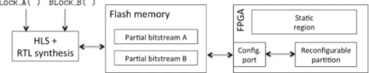
the resources can be important in that case. Actually the HLS tool does not share the resources efficiently although the modes are timewize mutually exclusive. Hardware reconfiguration: In dynamic partial reconfiguration, the FPGA is di-vided into several regions being static (the areas that are not modified) or re-configurable (the rere-configurable partitions). Each mode has its own partial bit-stream. The partial bitstreams are stored in a memory and a software processor controls which partial bitstream is loaded into the reconfigurable partition at a particular time. The reconfigurable partition size must cover the area of the largest mode. Figure 1 shows the example of the Hardware reconfiguration of two modes block A and block B. The two modes are processed separately using first HLS and then RTL synthesis to generate two partial bitstreams. Part of this flow can be automated, at least to have an estimation of the performance. The main advantage is that the modes share the same area. The drawback is the reconfiguration time that depends on the size of the partial bitstream. Algorithmic reconfiguration: For this kind of reconfiguration, the designer has to hand-code a dedicated processing block being intrinsically flexible. Signals are used to control the modes. Algorithmic optimizations should be done so that the HLS tool can share the resources between the modes.
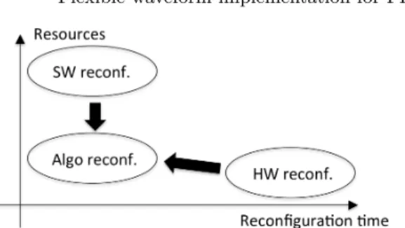
Fig. 2 shows the design tradeoff between the resources and the reconfiguration time when the three kinds of reconfiguration are considered. Algorithmic recon-figuration is used to decrease the resources compared to Software reconrecon-figuration and to decrease the reconfiguration time compared to Hardware reconfiguration. It provides the best performance in term of resources/reconfiguration time trade-off. However, depending on the processing blocks, time to code the algorithmic reconfiguration can be important compared to Software reconfiguration.
Fig. 2. Tradeoff between resources and reconfiguration time for the different reconfig-urations.
Based on these three kinds of reconfiguration, the design flow used in this work is shown in Fig. 3. The different modes of a processing block can be provided by hand-coding or using a HLS tool to generate different versions of a processing block by modifying synthesis constraints like throughput, latency, data size, etc. Such tools make it easy to explore a set of solutions via DSE [14][20][9] consid-ering a given architecture.
In Fig. 3, Performance constraints are user-defined constraints such as re-sources/area, reconfiguration time, throughput or latency. The Performance analysis compares the performance of the three paths to the user-defined con-straints. The basic idea is to first analyze the performance of the Software re-configuration and Hardware rere-configuration paths and to use the Algorithmic reconfiguration if the Performance constraints are not met.
We have experimented this design flow with the rapid prototyping of a flexible FFT. An architecture exploration was performed allowing the comparison of the three kinds of reconfiguration.
4 Building a flexible FFT
In this section, a flexible FFT is designed using the proposed approach. Ad-dressing LTE standard, the resulting FFT component should have six modes corresponding to these FFT sizes: {128, 256, 512, 1024, 1536, 2048}. To intro-duce the different kinds of reconfiguration, preliminary results are first given in Sections 4.1 and 4.2 with the design of a flexible FFT with two sizes: {128, 2048}. This design is based on two hand-coded FFT functions using the radix-2 Decimation-In-Time (DIT) algorithm which is the simplest and most common form of the Cooley-Tukey algorithm [7].
Experimental tools and setup: Vivado HLS 2013.3 is used for the high-level synthesis. DPR is setup with PlanAhead 14.6. The xc6vlx240tff1156 FPGA is targeted from Virtex 6 family as ML605 evaluation board will be used for future demonstration. Syntheses are based on a 100 MHz clock frequency.
4.1 Software reconfiguration
First, two functions for 128- and 2048-point FFTs have been hand-coded and synthesized separately (Block FFT128( ) and Block FFT2048( ) respectively). Then the FFT with 2 modes (128/2048) has been designed using Software recon-figuration: using Algorithm 1, a function Two Mode Block( ) is generated from Block FFT128( ) and Block FFT2048( ).
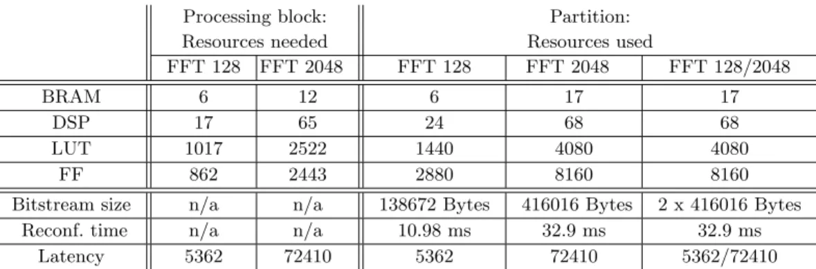
Table 1 shows the synthesis results and the latency (in number of clock cycles) of the three processing blocks. The resources are given with logical components such as the number of BRAM, DSP slices, LUT and FF.
As expected, Block FFT2048( ) requires more resources than Block FFT128( ): the number of BRAM to store cos and sin coefficients and input data is twofold and the number of DSP slices is 4 times more.
Except for the number of BRAM, Table 1 shows that the resources used by Two Mode Block( ) are (a little bit less than) the sum of the resources used by the two FFT blocks when synthesized separately. The HLS tool does not share the resources between the two functions although they are not executed at the same time. In this case, from the resources point of view, Software reconfiguration appears not to be an efficient solution to implement a flexible block. Latency is similar to mono-mode blocks.
Processing block Block FFT128( ) Block FFT2048( ) Two Mode Block( )
BRAM 6 12 12
DSP 17 65 82
LUT 1017 2522 3459
FF 862 2443 3241
Latency 5362 72410 5491/72411 Table 1. Performance of Software reconfiguration for a FFT with 2 modes (128/2048).
Processing block: Partition: Resources needed Resources used
FFT 128 FFT 2048 FFT 128 FFT 2048 FFT 128/2048
BRAM 6 12 6 17 17
DSP 17 65 24 68 68
LUT 1017 2522 1440 4080 4080
FF 862 2443 2880 8160 8160
Bitstream size n/a n/a 138672 Bytes 416016 Bytes 2 x 416016 Bytes Reconf. time n/a n/a 10.98 ms 32.9 ms 32.9 ms
Latency 5362 72410 5362 72410 5362/72410 Table 2. Performance for Hardware reconfiguration of a FFT with 2 modes (128/2048).
4.2 Hardware reconfiguration
The two functions Block FFT128( ) and Block FFT2048( ) are now used for Hardware reconfiguration. In Xilinx’s FPGAs [4], the functions to be dynami-cally placed are mapped into an area called a reconfigurable partition. Generally speaking, a partition has a rectangle shape and uses resources according to this area even if they are not needed.
Two partitions have been first generated using PlanAhead tool: one for the FFT 128 only and one for the FFT 2048 only. Table 2 shows the resources used by these partitions. Bitstream sizes are also given. Because FFT 128’s partition uses less logical components than FFT 2048’s one, it is smaller than FFT 2048’s one. The reconfiguration time depends on the bitstream size so the reconfigu-ration time for FFT 128 is smaller than FFT 2048’s one. Reconfigureconfigu-ration time is computed from PRCC tool (Partial Reconfiguration Cost Calculator) from Technical University of Crete [3] assuming that the reconfiguration controller is an on-chip MicroBlaze processor1.
For comparison, Table 2 also shows the resources needed by FFT 128 and FFT 2048 when they are placed as static logic (i.e. not as a reconfigurable module, so resources needed are same as in Table 1).
To perform the DPR of the 2 functions, a third partition called FFT 128/2048 in Table 2 has been defined. In this case, the two functions are placed on the same partition, i.e. on the same area of the FPGA. For each type of logical component, the resources used by this partition are based on the more costly case. In our case, FFT 2048 partition always needs the largest number of resources whatever the kind of logical component. Thus the resulting FFT 128/2048 partition is based on the FFT 2048 partition.
Reconfigurable partition’s latency is equal to the latency of the function when synthesized alone onto a static region. The hardware reconfiguration needs 32.9 ms to switch from one mode to the other one whereas only one clock cycle is required with Software reconfiguration. It means many OFDM symbols will be lost in practice when changing the mode with hardware reconfiguration.
1
Higher throughput up to 400 MBytes/s may be reached using a dedicated controller so that reconfiguration time can be reduced.
4.3 Algorithmic reconfiguration
The FFT for LTE standard should have six modes: {128, 256, 512, 1024, 1536, 2048}. Based on the previous results, a Software reconfiguration will generate a huge component as the resources are not shared. Hardware reconfiguration makes re-source sharing possible but may require a long reconfiguration time. In this sec-tion, we first present a power-of-two point FFT for algorithmic reconfiguration to share the resources between its different modes. Then, a FFT 1536 function is presented. Sharing the resources of these 2 functions is discussed.
Power-of-two point FFT for algorithmic reconfiguration: The power-of-two point FFT has 5 modes {128, 256, 512, 1024, 2048}. A dedicated control signal is used to decide the mode and the HLS tool deals with the FFT size as a variable. Indeed, as presenting in Algorithm 2, FFT size and FFT stages are calculated based on the control signal value. When FFT size and FFT stages are determined, a standard three-loop structure for the FFT based on radix-2 is computed. The first loop determines the stage. The second loop chooses butterflies with the same twiddle factor at each stage. Last loop computes all the chosen butterflies. This algorithmic reconfiguration generates a Block FFTpow2() function with only one main FFT core for the five different modes. With this function, the resources should be approximately the ones used by the largest FFT (i.e. 2048). 1536-point FFT: By applying the Cooley-Tukey algorithm [7] for a FFT size of 1536, the Block FFT1536( ) function can be generated using three Block FFT512( ) functions and one radix-3 function [11] as shown in Fig 4. First, the 1536 inputs of the FFT are split into three parts. Those parts are computed as three 512-point FFTs independently. Then, while the first part is kept as it is, the second and the third ones are multiplied by twiddles factors. Last, the radix-3 function is applied to compute the final results.
Resource sharing may theoretically be done between Block FFT512( ) func-tions of the 1536-point FFT and the power-of-two point FFT because they are
Algorithm 2 Algorithmic reconfiguration for the power-of-two point FFT.
function Block FFTpow2(inputs, outputs, control) . 0 ≤ control ≤ 4 FFT size max = 2048
FFT stages max = 11
FFT size = FFT size max >> control . FFT size = FFT size max
2control
FFT stages= FFT stages max - control
Bit reverse( ) . re-range the order of bits before calculating for i = 0 to FFT stages do
Calculate index( ) . choose the stage, prepare for possible twiddles for j = 0 to FFT size/2 do
Computing twiddles( ) . determine coefficients for radix 2 for k = 0 to FFT size/2 do
Radix 2(inputs, outputs) end function
Fig. 4. Functional description of Block FFT1536( ) function.
both based on the radix-2 algorithm. On the contrary, the Block Radix3( ) function is based on radix-3 thus it can not share resources.
5 Performance results
This section presents the architectural exploration of a flexible FFT for LTE standard. First, design space will be explored for the function Block FFTpow2(). Then, the combination between Block FFTpow2( ) and Block FFT1536( ) will be addressed using Software and Hardware reconfigurations.
5.1 Design space exploration of the power-of-two point FFT
In order to generate a flexible FFT that respects the design constraints (area, la-tency, throughput, . . .), HLS allows the DSE of a processing block by using com-pilation directives. This part presents the DSE of the function Block FFTpow2(). Several directives are made available on a typical HLS tool (e.g. memory map-ping, pipeline, loop unrolling, inlining, . . .). They make it possible to optimize the design for area or latency. In this study, because of the loop structures and the data dependencies of the FFT, loop unrolling is used. Loop unrolling reduces the total loop iterations by duplicating (with a factor U) the loop body so that
we can tradeoff between area and latency.
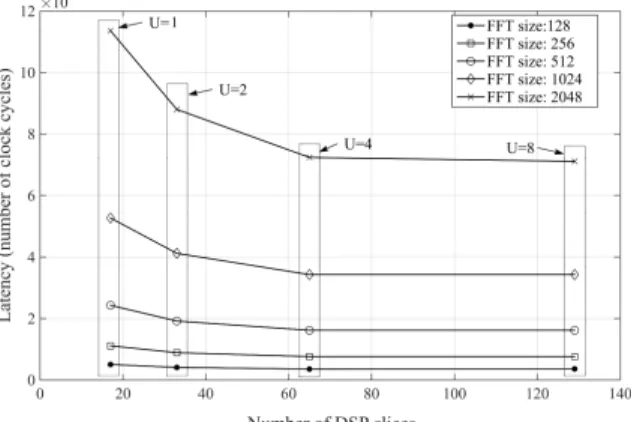
Figure 5 shows the latency of Block FFTpow2( ) processing block as a function of the number of DSP slices. In practice, four multi-mode components have been generated by varying the unroll factor U. Each component is characterized by its numbers of DSP slices. The number of DSP slices increases with the unroll factor while the latency decreases with the unroll factor. One’s can see a floor effect appears in Figure 5. Due to the BRAM accesses (read and write data from/to memory) that reach their bounds for U=4, increasing the number of DSP resources is not useful in practice.
The same behavior is also obtained for the number of LUT and FF. Thus U=4 seems to be a good tradeoff between number of resources and latency.
5.2 Proposed flexible FFT implementations for LTE standard
Performance of the multi-mode FFT with software reconfiguration: Software reconfiguration is applied first to design the FFT with 6 modes for LTE. Using Algorithm 1, a Multi Mode Block LTE( ) function is generated from the two functions Block FFTpow2( ) and Block FFT1536( ). Table 3 shows the synthesis results and latency (in number of clock cycles) of the three processing blocks. U=4 is used for Block FFTpow2( ). The resources used by Multi Mode Block LTE( ) are almost the sum of the resources used by Block FFTpow2( ) and Block FFT1536( ) when synthesized separately. As ob-served in Section 4.1, the HLS tool does not share the resources between the two functions even if they are not executed at the same time.
Performance of the multi-mode FFT with hardware reconfiguration: Hardware reconfiguration is now applied on the two functions Block FFTpow2( ) and Block FFT1536( ). Two partitions are first generated: one for the power-of-two point FFT only and one for the FFT 1536 only. Then, a partition is finally cre-ated for the DPR of the 2 FFTs.
Table 4 shows the synthesis results. The partition for FFT 1536 is smaller than the power-of-two point FFT’s one. Actually, number of BRAMs is greater but function Block FFT1536( ) uses less DSP slices than Block FFTpow2( ) so that its area is smaller. Thus, when combining the 2 FFTs into one partition, the resulting partition is based on power-of-two point FFT’s partition.
Processing block Block FFTpow2( ) Block FFT1536( ) Multi Mode Block LTE( )
BRAM 12 14 26
DSP 65 40 103
LUT 2553 3054 5256
FF 2497 2010 4299
Latency cf. Fig.5 - U=4 52198 cf. Fig.5/52198 Table 3. Performance of a FFT for LTE standard with Software reconfiguration.
Processing block: Partition: Resources needed Resources used
Pow.-of-two FFT FFT 1536 Pow.-of-two FFT FFT 1536 FFT for LTE
BRAM 12 14 17 14 17
DSP 65 40 68 56 68
LUT 2553 3054 4080 3360 4080
FF 2497 2010 8160 6720 8160
Bitstream size n/a n/a 416016 Bytes 277344 Bytes 2 x 416016 Bytes Reconf. time n/a n/a 32.9 ms 21.96 ms 32.9 ms
Latency cf. Fig.5 - U=4 52198 cf. Fig.5 - U=4 52198 cf. Fig.5/52198 Table 4. Performance of a FFT for LTE standard with Hardware reconfiguration.
Compared with Software reconfiguration, the multi-mode FFT based on hard-ware reconfiguration uses less resources (BRAM and DSP are the more area costly logical components). When the FFT size has to be modified but is still a power of two, in both cases only one clock cycle is required to reconfigure. However, 32.9 ms are required to reconfigure when switching from a 1536-point FFT and a power-of-two point FFT (or vice versa) with hardware reconguration whereas only one clock cycle is required with Software reconfiguration.
6 Conclusion
This paper presents a methodology for the implementation of run-time recon-figuration in the context of FPGA-based SDR. The proposed design flow allows the exploration between dynamic partial reconfiguration and control signal based multi-mode design. This architectural tradeoff relies upon HLS and its associ-ated design optimizations.
A flexible FFT for LTE standard is implemented as a case study. The proposed component combines both DPR (to deal with FFT size of 1536) and algorithmic reconfiguration (when FFT size is a power of two). Synthesis results show the tradeoff that could be achieved between the reconfiguration time and the FPGA resource utilization. Future work is to explore the implementation of other pro-cessing functions and the automation of the design flow.
References
1. GNU Radio: The free and open software radio ecosystem. www.gnuradio.org. 2. Increasing Design Functionality with Partial and Dynamic Reconfiguration in
28-nm FPGAs, Altera white paper, WP-01137-1.0, www.altera.com.
3. Kyprianos Papadimitriou, Microprocessor and Hardware Laboratory, Technical University of Crete. Partial Reconfiguration Cost Calculator. URL: http://users. isc.tuc.gr/~kpapadimitriou/prcc.html.
4. Partial Reconfiguration User Guide, UG702 (v14.1), www.xilinx.com, 2012. 5. E. Casseau and B. Le Gal. Design of Multi-Mode Application-Specific Cores Based
6. Jienan Chen, Jianhao Hu, Shuyang Lee, and G.E. Sobelman. Hardware Efficient Mixed Radix-25/16/9 FFT for LTE Systems. Very Large Scale Integration (VLSI) Systems, IEEE Transactions on, 23(2):221–229, February 2015.
7. James W. Cooley and John W. Tukey. Mathematics of Computation, chapter An algorithm for the machine calculation of complex Fourier series, pages 297–301. American Mathematical Society, 1965.
8. M. Cummings and S. Haruyama. FPGA in the Software Radio. IEEE Communi-cations Magazine, 37(2):108–112, February 1999.
9. M. Gautier, G.S. Ouedraogo, and O. Sentieys. Design Space Exploration in an FPGA-Based Software Defined Radio. In Euromicro Conference on Digital System Design (DSD), pages 22–27, Verona, Italy, August 2014.
10. Antoni Gelonch, Xavier Revs, Vuk Marojevik, and Ramon Ferr´us. P-HAL: a Mid-dleware for SDR applications. SDR Forum Technical Conference, November 2005. 11. Freescale Semiconductor Incorporated. Software Optimization of DFTs and IDFTs
Using the StarCore SC3850 DSP Core. Application Note AN3980, 2009.
12. G. Jianxin, Y. Xiaohui, G. Jun, and L. Quan. The Software Communication Archi-tecture: Evolutions and Trends. IEEE Conference on Computational Intelligence and Industrial Applications (PACIIA), November 2009.
13. J. F. Jondral. Software-defined radio: Basics and evolution to cognitive radio. EURASIP Journal on Wireless Communications and Networking, 3, 2005. 14. Y. Le Moullec, J.-P. Diguet, N. Ben Amor, T. Gourdeaux, and J.-L. Philippe.
Algorithmic-level specification and characterization of embedded multimedia ap-plications with design trotter. Journal of VLSI signal processing systems for signal, image and video technology, 42(2):185–208, 2006.
15. E. Lemoine and D. Merceron. Run time reconfiguration of FPGA for scanning genomic databases. In IEEE Symposium on FPGAs for Custom Computing Ma-chines, pages 90–98, April 1995.
16. Y. Lin, R. Mullenix, M. Woh, S. Mahlke, T. Mudge, A. Reid, and K. Flautner. SPEX: A Programming Language for Software Defined Radio. In Software De-fined Radio Technical Conference and Product Exposition (SDR-Forum), Novem-ber 2006.
17. G.-S. Ouedraogo, M. Gautier, and O. Sentieys. A frame-based Domain-Specific Language for rapid prototyping of FPGA-based Software-Defined Radios. EURASIP Journal on Advances in Signal Processing, 2014(1):164, November 2014. 18. G. S. Ouedraogo, M. Gautier, and O. Sentieys. Frame-based Modeling for Auto-matic Synthesis of FPGA-Software Defined Radio. IEEE International Conference on Cognitive Radio Oriented Wireless Networks and Communications (CROWN-COM), June 2014.
19. T. Pitkanen and J. Takala. Low-power application-specific processor for FFT computations. In IEEE International Conference on Acoustics, Speech and Signal Processing (ICASSP), pages 593–596, April 2009.
20. B. So, M. W. Hall, and P. C. Diniz. A compiler approach to fast hardware design space exploration in FPGA-based systems. In Proceedings of the ACM SIGPLAN Conference on Programming language design and implementation (PLDI), pages 165–176, New York, USA, 2002.
21. E. D. Willink. The Waveform Description Language: Moving from Implementation to Specification. IEEE Military Communications Conference (MILCOM), 2001. 22. Chia-Hsiang Yang, Tsung-Han Yu, and D. Markovic. Power and Area Minimization
of Reconfigurable FFT Processors: A 3GPP-LTE Example. Solid-State Circuits, IEEE Journal of, 47(3):757–768, March 2012.