HAL Id: hal-00488065
https://hal.archives-ouvertes.fr/hal-00488065
Submitted on 10 May 2011HAL is a multi-disciplinary open access archive for the deposit and dissemination of sci-entific research documents, whether they are pub-lished or not. The documents may come from teaching and research institutions in France or abroad, or from public or private research centers.
L’archive ouverte pluridisciplinaire HAL, est destinée au dépôt et à la diffusion de documents scientifiques de niveau recherche, publiés ou non, émanant des établissements d’enseignement et de recherche français ou étrangers, des laboratoires publics ou privés.
170 Gbit/s transmission in an erbium-doped waveguide
amplifier on silicon
Jonathan D. B. Bradley, Marcia Costa E Silva, Mathilde Gay, Laurent
Bramerie, Alfred Driessen, Kerstin Wörhoff, Jean-Claude Simon, Markus
Pollnau
To cite this version:
Jonathan D. B. Bradley, Marcia Costa E Silva, Mathilde Gay, Laurent Bramerie, Alfred Driessen, et al.. 170 Gbit/s transmission in an erbium-doped waveguide amplifier on silicon. Optics Express, Optical Society of America - OSA Publishing, 2009, 17 (24), pp.22201-22208. �10.1364/OE.17.022201�. �hal-00488065�
170 Gbit/s transmission in an erbium-doped waveguide
amplifier on silicon
Jonathan D. B. Bradley,1,* Marcia Costa e Silva,2 Mathilde Gay,2 Laurent Bramerie,2
Alfred Driessen,1 Kerstin Wörhoff,1 Jean-Claude Simon,2 and Markus Pollnau1
1
Integrated Optical Microsystems Group, MESA+ Institute for Nanotechnology, University of Twente, P.O. Box 217, 7500 AE Enschede, The Netherlands
2
FOTON Laboratory, CNRS UMR 6082 / PERSYST Platform,University of Rennes 1 / ENSSAT, 6 Rue de Kerampont, BP 80518 22305 Lannion Cedex, France
*
Corresponding author: j.d.b.bradley@ewi.utwente.nl
Signal transmission experiments were performed at 170 Gbit/s in an integrated Al2O3:Er3+ waveguide amplifier to investigate its potential application in high-speed photonic integrated circuits. Net internal gain of up to 11 dB was measured for a continuous-wave 1532 nm signal under 1480 nm pumping, with a threshold pump power of 4 mW. A differential group delay of 2 ps between the TE and TM fundamental modes of the 5.7-cm-long amplifier was measured. When selecting a single polarization open eye diagrams and bit error rates equal to those of the transmission system without the amplifier were observed for a 1550 nm signal encoded with a 170 Gbit/s return-to-zero pseudo-random 27-1 bit sequence. 2008 Optical Society of America
OCIS codes: 130.3120 (Integrated optics devices), 130.3130 (Integrated optics
1. Introduction
One of the key driving forces behind integrated optics, and particularly silicon photonics, is the potential for higher data transmission rates compared to integrated electronic circuits [0]. Data rates as high as 160 Gbit/s have been demonstrated in long-haul optical fiber networks [2] and in the future transmission at this speed can also be expected at the chip level. In such integrated photonic circuits, several enabling elements would be required, including an amplifier to boost the optical signal at various stages. Semiconductor optical amplifiers (SOAs) are well established as packaged components. However fabrication of such devices is complex, requiring many processing steps, and for incorporation of a SOA between silicon-based passive components hybrid integration methods are required. In addition, due to their short carrier lifetimes of ~50 ps, when they are operated in the saturated or quasi-saturated gain regime SOAs exhibit transient gain suppression and recovery which is dependent on both the bit rate and the bit sequence [3]. This can result in cross-talk between different wavelength channels when amplifying wavelength division multiplexed (WDM) signals. Alternatively, planar erbium-doped waveguide amplifiers (EDWA) [4] offer a potential solution for amplification at high speed on a chip. Er-doped amplifiers with their long excited-state lifetime of ~10 ms and accordingly longer gain recovery time do not exhibit such transient channel cross-talk. EDWAs can be deposited directly on thermally oxidized silicon or other materials allowing all-optical signal enhancement with a straightforward process flow [5]. Furthermore, the widespread availability of compact, low-cost laser diode pump sources begins to make such devices more attractive. Compared to other EDWA materials, Al2O3:Er3+ offers increased integration potential. Because of its relatively high refractive index contrast (∆n ≈ 0.2 compared to the SiO2 cladding), more compact waveguide cross-sections and thus higher pump intensities can be achieved, allowing higher integration
density and reducing pump power requirements [6]. Recently we have demonstrated significantly improved continuous-wave gain with a wavelength range of 80 nm and 2 dB/cm at the 1532 nm peak in this material [7].
In the past, transmission experiments at up to 10 Gbit/s using an EDWA have been carried out [8-10] and a packaged photoreceiver using an EDWA for 40 Gbit/s applications has also been reported [11]. In this letter we demonstrate amplification at 170 Gbit/s in an Al2O3:Er3+ EDWA deposited on thermally oxidized silicon.
2. Al2O3:Er3+ channel waveguide gain
A 5.7-cm-long reactively co-sputtered Er-doped aluminum oxide (Al2O3:Er3+) straight channel waveguide amplifier was fabricated on a thermally oxidized silicon substrate. The fabrication procedure has been reported elsewhere [12, 13]. The cross-sectional dimensions of the ridge-type channel waveguide were 0.9 µm × 4.0 µm with an etch depth of approximately 50 nm. The uncladded waveguide was single mode at wavelengths of 1480 nm and above. The doping concentration, uniform throughout the Al2O3:Er3+ core layer, was 2.1
× 1020 cm-3 [7].
Prior to transmission experiments, the continuous-wave small-signal gain of the amplifier was measured at 1532 nm (the 4I13/2 → 4I15/2 Er transition gain peak) and 1550 nm (the wavelength at which transmission experiments were performed). Pump light from a 1480 nm Raman laser source and signal light at 1532 nm or 1550 nm from a tunable laser were combined using a WDM fiber multiplexer (MUX) and coupled to and from the chip via lensed fibers [14]. Both microlensed fibers have a mode-field diameter of 2.9 µm at 1/e2 of the intensity profile. This mode-field diameter appears to be a good compromise to the asymmetry of the waveguide. At the output, the residual pump light and amplified
spontaneous emission (ASE) were filtered using a 0.25 nm tunable bandpass filter and the signal power was measured with an optical power meter. Both co- and counter-propagating pump cases were investigated. The internal net small signal gain was calculated by subtracting the total propagation loss from the measured signal enhancement with pump on and pump off. The total small-signal propagation loss was calculated at each wavelength using the known background loss of 0.13 dB/cm, calculated confinement of the signal light within the Al2O3:Er3+ waveguide core (85%) and measured 4I15/2 → 4I13/2 absorption cross-sections [7]. The residual pump light and ASE were measured by shifting the bandpass filter 2 nm from the signal wavelength and determined to be negligible (> 20 dB lower than the amplified signal).
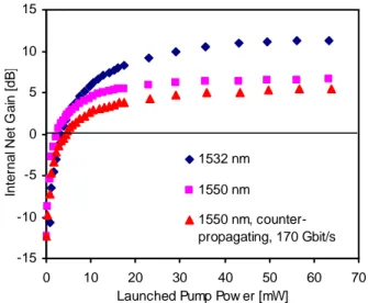
The resulting gain vs. pump power curves are shown in Fig. 1. The average gain for both TE- and TM-polarized signal light is shown, since similar signal enhancement was measured for each polarization (± 0.2 dB). In the co-propagating case, up to 11 dB total internal net gain at 1532 nm was measured for a launched pump power of 63 mW, while 6.6 dB gain was measured at 1550 nm. The threshold launched pump power for internal net gain was 4 mW and 3 mW at 1532 nm and 1550 nm, respectively. For a launched pump power of 65 mW constant internal net gain was measured when varying the launched signal power from 1 µW to 1 mW, demonstrating unsaturated gain for launched signal powers in this range. While high internal net gain was demonstrated, external fiber-chip-fiber net gain was not obtained, because the amplifier was designed for on-chip amplification, hence achieving low fiber-chip coupling loss was not considered in the design. However, with improved lensed fibers and appropriate waveguide design fiber-chip coupling losses on the order of 1 dB/facet are predicted, thus principally also allowing for fiber-chip-fiber net gain. Furthermore, in a longer amplifier internal net gain of more than 20 dB is expected across the entire C-band wavelength range (1525-1565 nm) [7]. The net internal gain measured at 1550
nm using a counter-propagating pump setup and the 170 Gbit/s modulated signal is also shown in Fig. 1. A higher threshold pump power is observed for counter-propagating pumping as compared to the co-propagating pump measurement. The difference in the two curves is probably due to a difference in pump coupling efficiency between the two lensed fibers. Net gain of up to 6.3 dB at 1550 nm was achieved in the counter-propagating setup when the launched pump power was increased to 110 mW.
-15 -10 -5 0 5 10 15 0 10 20 30 40 50 60 70
Launched Pump Pow er [mW]
In te rn a l N e t G a in [ d B ] 1532 nm 1550 nm 1550 nm, counter-propagating, 170 Gbit/s
Fig. 1. Internal net small signal gain at 1532 nm and 1550 nm (for co-propagating pumping and counter-propagating pumping with 170 Gbit/s signal) as a function of launched 1480 nm pump power
3. 170 Gbit/s transmission measurements
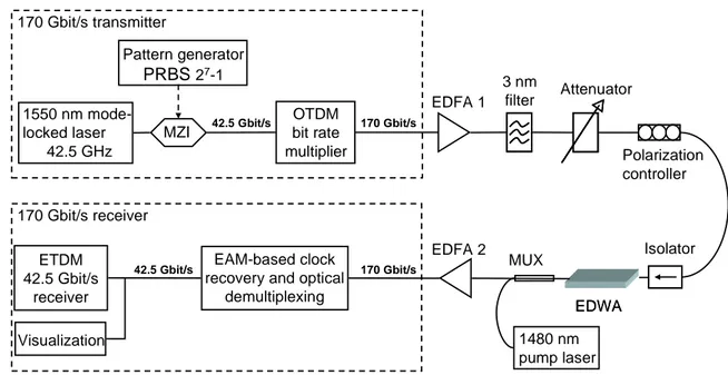
Transmission experiments were performed at a bit rate of 170 Gbit/s on the PERSYST platform. The experimental setup is depicted schematically in Fig. 2. The transmitter was composed of a 42.5 GHz optical clock generated from a filtered and chirp-compensated quantum dash Fabry-Perot mode-locked laser source at 1550 nm [15, 16]. Following this, a
LiNbO3 Mach-Zehnder Interferometer (MZI) was modulated electronically by a pattern generator to obtain a 42.5 Gbit/s 27-1 return-to-zero pseudo-random bit sequence (PRBS). The transmitter ended with an optical time division multiplexing (OTDM) bit rate multiplier that multiplexed four delayed versions of the signal, resulting in a 170 Gbit/s data stream consisting of pulses with a full width at half maximum (FWHM) of 1.5 ps. An erbium-doped fiber amplifier (EDFA) was then used to boost the signal followed by an optical attenuator and polarization controller to adjust the amount of power and the polarization of the signal light coupled to the device, respectively. An optical isolator was used to eliminate any back-scattered pump or signal light. The 1550 nm 170 Gbit/s signal was coupled to and from the chip via the microlensed fibers. 1480 nm pump light from a Raman pump laser source was coupled to the chip in a counter-propagating approach using a fiber multiplexer (MUX). A reverse-pumping scheme was selected because it simplified the transmission setup by eliminating the need for filtering of residual pump light in front of the receiver. The transmitted signal was amplified by an EDFA before entering the receiver part of the setup. The first part of the receiver was composed of a 170 to 42.5 Gbit/s optical demultiplexer and an optical clock recovery based on an electro-optic absorption modulator (EAM) and phase-locked loop. Following this, the signal light was detected by a 42.5 Gbit/s electrical time division demultiplexing receiver (ETDM). An optical sampling oscilloscope (with 1 ps resolution) was used for visualization.
MZI
EAM-based clock recovery and optical
demultiplexing EDWA EDWA MUX 1480 nm pump laser EDFA 1 OTDM bit rate multiplier 42.5 Gbit/s 170 Gbit/s 1550 nm mode-locked laser 42.5 GHz Polarization controller Visualization 42.5 Gbit/s 170 Gbit/s ETDM 42.5 Gbit/s receiver Isolator Attenuator EDFA 2 Pattern generator PRBS 27-1 170 Gbit/s receiver 170 Gbit/s transmitter 3 nm filter
Fig. 2. Experimental setup for 170 Gbit/s transmission measurements
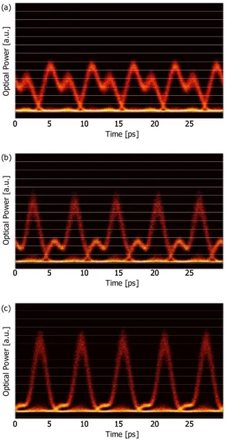
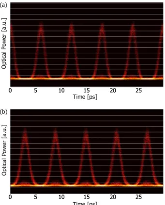
In initial transmission experiments with a randomly polarized signal it was observed that two polarization modes were present. In order to investigate the polarization dependence of the amplifier, the differential group delay (DGD) between the fundamental TE and TM modes in the pumped and unpumped EDWA was measured using a continuous tunable laser source and a DGD analyzer. In both cases the DGD was found to be approximately 2 ps corresponding to a waveguide birefringence of ~7 x 10⁻³. The impact of DGD on the 170 Gbit/s signal was also clearly observed in the eye diagram as shown in Figs. 3 (a-c), by varying the polarization controller state. This polarization dependence should not affect the system when used in a transmitter in a photonic integrated circuit, for instance, even though it would affect signal quality in an in-line use of the device. However, by careful design of the waveguides the birefringence can be largely reduced [17] so that polarization-independent amplification even at these bit rates can be obtained. For all bit error rate (BER) measurements a single polarization state was selected by adjusting the polarization controller on one fundamental mode. Typical eye diagrams without the EDWA and with the EDWA
and a single polarization are shown in Figs. 4 (a) and (b), respectively. The eye pattern is open and the pulse FWHM is 2 ps in both cases.
0 5 10 15 20 25 Time [ps] O p ti ca l P o w e r [a .u .] 0 5 10 15 20 25 0 5 10 15 20 25 Time [ps] O p ti ca l P o w e r [a .u .] 0 5 10 15 20 25 Time [ps] O p ti ca l P o w e r [a .u .] 0 5 10 15 20 25 0 5 10 15 20 25 Time [ps] O p ti ca l P o w e r [a .u .] 0 5 10 15 20 25 Time [ps] O p ti ca l P o w e r [a .u .] 0 5 10 15 20 25 0 5 10 15 20 25 Time [ps] O p ti ca l P o w e r [a .u .] (b) (a) (c)
Fig. 3. Transmission eye diagrams for different polarization states of the 170 Gbit/s signal coupled to the EDWA. In each image two overlayed pulse trains are visible as a result of differential group delay between the fundamental TE and TM polarized modes supported by the EDWA. The input signal polarization state was adjusted such that in (a) both modes propagated with almost equal intensity, (b) one mode was more strongly excited, and (c) almost a single polarization mode was excited.
0 5 10 15 20 25 0 5 10 15 20 25 Time [ps] O p ti ca l P o w e r [a .u .] O p ti ca l P o w e r [a .u .] Time [ps] (b) (a) 0 5 10 15 20 25 0 5 10 15 20 25
Fig. 4. Transmission eye diagrams at 170 Gbit/s (a) without EDWA and (b) with EDWA and a launched signal power of 0.5 mW and counter-propagating pump power of 65 mW
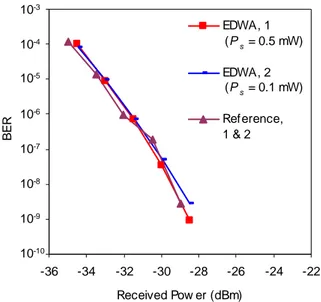
In order to determine the compatibility of the device in a telecommunication application, BER assessments were performed on the device. The BER was measured as a function of the input power on the ETDM 42.5 Gbit/s receiver for 0.5 mW and 0.1 mW of signal power and a pump power of 65 mW launched into the EDWA. A reference was measured with the same input power in EDFA 2 as with the EDWA included in order to take into account the fiber-to-fiber losses (~10 dB when pumped) of the EDWA. The results are shown in Fig. 5. For each input signal power, the curve with the EDWA is superposed with the reference, showing that when the polarization state is properly adjusted, the EDWA does not add any penalty to the system. A minimum launched signal power of 0.1 mW was investigated in this setup in order to ensure sufficient power reached the receiver. However, based on the negligible ASE in the
small-signal gain measurements and with improved coupling losses, no penalties can also be expected in the EDWA for launched signal powers in the 1-10 µW range.
-36 -34 -32 -30 -28 -26 -24 -22 Received Pow er (dBm) B E R EDWA, 1 EDWA, 2 Reference, 1 & 2 10-10 10-9 10-8 10-7 10-6 10-5 10-4 10-3 (Ps = 0.5 mW) (Ps = 0.1 mW)
Fig. 5. 170 Gbit/s BER measurements for different launched signal powers Ps and a launched
pump power of 65 mW as a function of the input power at the 42.5 Gbit/s receiver. A reference measurement with EDWA removed and identical optical power launched into the receiver is also shown.
4. Conclusions
Net internal gain of up to 11 dB at 1532 nm and data transmission at 170 Gbit/s at 1550 nm have been demonstrated in an integrated Al2O3:Er3+ amplifier when pumping at 1480 nm. Despite a DGD of 2 ps between the two guided polarization modes of the amplifier, no BER power penalty was observed at 170 Gbit/s by injecting the signal in a single fundamental polarization state. The ability to amplify signals at high data rates, when combined with straightforward fabrication techniques and the possibility to integrate with various materials,
confirm such amplifiers as potential components in future high-speed photonic integrated circuits.
Acknowledgments
We would like to thank the “Centre Commun Lannionais d’Optique” of CNRS Foton for the fabrication of the microlensed fibers. This work was supported by funding through the European Union's Sixth Framework Programme (Specific Targeted Research Project “PI-OXIDE”, contract no. 017501) and the European FP6 Network of Excellence ePIXnet High Speed Characterisation Platform.
References
1. Y. Kang, H.-D. Liu, M. Morse, M. J. Paniccia, M. Zadka, S. Litski, G. Sarid, A. Pauchard, Y.-H. Kuo, H.-W. Chen, W. Sfar Zaoui, J. E. Bowers, A. Beiling, D. C. McIntosh, X. Zheng, and J. C. Campbell, “Monolithic germanium/silicon avalanche photodiodes with 340 GHz gain-bandwidth product,” Nature Photon. 3(1), 59-63 (2009). 2. S. Ferber, R. Ludwig, C. Boerner, C. Schubert, C. Schmidt-Langhorst, M. Kroh, V.
Marembert, and H. G. Weber, “160 Gbit/s DPSK transmission over 320 km fibre link with high long-term stability,” Electron. Lett. 41(4), 200-202 (2005).
3. L. H. Spiekman, “Semiconductor optical amplifiers,” in Optical Fiber Telecommunications Volume IVA, I. P. Kaminow and T. Li, eds. (Academic Press, 2002),
pp. 699-731.
4. T. Kitagawa, K. Hattori, K. Shuto, M. Yasu, M. Kobayashi, and M. Horiguchi, “Amplification in erbium-doped silica-based planar lightwave circuits,” Electron. Lett. 28(19), 1818-1819 (1992).
5. D. R. Zimmerman and L. H. Spiekman, “Amplifiers for the masses: EDFA, EDWA, and SOA amplets for metro and access networks,” J. Lightwave Technol. 22(1), 63-70 (2004). 6. G. N. van den Hoven, R. J. I. M. Koper, A. Polman, C. van Dam, K. W. M. van Uffelen, and M. K. Smit, “Net optical gain at 1.53 µm in Er-doped Al2O3 waveguides on silicon,” Appl. Phys. Lett. 68(14), 1886-1888 (1996).
7. J. D. B. Bradley, L. Agazzi, D. Geskus, F. Ay, K. Wörhoff, and M. Pollnau, “Gain bandwidth of 80 nm and 2 dB/cm peak gain in Al2O3:Er3+ optical amplifiers on silicon,” submitted.
8. G. Nykolak, M. Haner, P. C. Becker, J. Shmulovich, and Y. H. Wong, “Systems evaluation of an Er3+-doped planar waveguide amplifier,” IEEE Photon. Technol. Lett. 5(10), 1185-1187 (1993).
9. J. M. P. Delavaux, S. Granlund, O. Mizuhara, L. D. Tzeng, D. Barbier, M. Rattay, F. SaintAndre, and A. Kevorkian, “Integrated optics erbium-ytterbium amplifier system in 10-Gb/s fiber transmission experiment,” IEEE Photon. Technol. Lett. 9(2), 247-249 (1997).
10.J. Shmulovich, A. J. Bruce, G. Lenz, P. B. Hansen, T. N. Nielsen, D. J. Muehlner, G. A. Bogert, I. Brener, E. J. Laskowski, A. Paunescu, I. Ryazansky, D. C. Jacobson, and A. E. White, “Integrated planar waveguide amplifier with 15 dB net gain at 1550 nm,” in
Optical Fiber Communication Conference and the International Conference on Integrated Optics and Optical Fiber Communication, OSA Technical Digest (Optical
Society of America, 1999), paper PD42.
11.S. Demiguel, N. Sahri, M. Hartlaub, F. Blache, H. Gariah, S. Vuiye, D. Carpentier, D. Barbier, and J. C. Campbell, “Low-cost photoreceiver integrating an EDWA and waveguide PIN photodiode for 40 Gbit/s applications,” Electron. Lett. 43(1), 51-52 (2007).
12.K. Wörhoff, J. D. B. Bradley, F. Ay, D. Geskus, T. Blauwendraat, and M. Pollnau, “Reliable low-cost fabrication of low-loss Al2O3:Er3+ waveguides with 5.4-dB optical gain,” IEEE J. Quantum Electron. 45(5), 454-461 (2009).
13.J. D. B. Bradley, F. Ay, K. Wörhoff, and M. Pollnau, “Fabrication of low-loss channel waveguides in Al2O3 and Y2O3 layers by inductively coupled plasma reactive ion etching,” Appl. Phys. B 89(2-3), 311-318 (2007).
14.M. Thual, D. Malarde, B. Abhervé-Guégen, P. Rochard, P. Chanclou, “Truncated Gaussian beams through microlenses based on a graded-index section,” Opt. Eng. 46(1), 015402/1-12 (2007).
15.M. Costa e Silva, H. Ramanitra, M. Gay, L. Bramerie, S. Lobo, M. Joindot, J. C. Simon, A. Shen, and G.-H. Duan, “Wavelength tunability assessment of a 170 Gbit/s transmitter using a quantum dash Fabry Perot mode-locked laser,” to be presented at the 35th European Conference on Optical Communication, Vienna, Austria, 20-24 September, 2009.
16.F. Lelarge, B. Dagens, J. Renaudier, R. Brenot, A. Accard, F. van Dijk, D. Make, O. Le Gouezigou, J.-G. Provost, F. Poingt, J. Landreau, O. Drisse, E. Derouin, B. Rousseau, F. Pommereau, and G.-H. Duan, “Recent advances on InAs/InP quantum dash based semiconductor lasers and optical amplifiers operating at 1.55 µm,” IEEE J. Select. Topics Quantum Electron. 13(1), 111-127 (2007).
17.K. Wörhoff, B. J. Offrein, P. V. Lambeck., G. L. Bona, and A. Driessen, “Birefringence compensation applying double-core waveguiding structures,” IEEE Photon. Technnol. Lett. 11(2), 206-208 (1999).