Thermal admittance spectroscopy of Mg-doped GaN Schottky diodes
N. D. Nguyen,a)M. Germain, and M. Schmeits
Institut de Physique, Universite´ de Lie`ge, B5, B-4000 Lie`ge, Belgium
B. Schineller and M. Heukenb)
AIXTRON AG, D-52072 Aachen, Germany
共Received 15 February 2001; accepted for publication 19 April 2001兲
Thermal admittance spectroscopy measurements at temperatures ranging from room temperature to 90 K are performed on Schottky structures based on Mg-doped GaN layers grown by metalorganic vapor phase epitaxy on sapphire. The analysis of the experimental data is made by a detailed theoretical study of the steady-state and small-signal electrical characteristics of the structures. Numerical simulations are based on the solution of the basic semiconductor equations for the structure consisting of two Schottky diodes connected back to back by a conduction channel formed by the GaN layer. The description explicitly includes the Mg-related acceptor level, with its temperature- and position-dependent incomplete occupation state, leading to a dynamic exchange with the valence band. It fully reproduces the variations with temperature of the capacitance– frequency and conductance over frequency curves, allowing to give for all temperature ranges the origin of the various contributions to the junction capacitance and of the microscopic mechanisms responsible for the capacitance–frequency cutoff. Series resistance effects are shown to be dominant at temperatures above 230 K, whereas the Mg-related acceptor level governs the electrical behavior below 230 K. The existence of a second acceptor level with an activation energy of several tens of meV is revealed from the analysis of the characteristics at low temperature. An optimized fitting procedure based on the comparison of the electrical characteristics obtained from the numerical simulations to the experimental data allows one to determine the microscopic parameters describing the structure, among which the acceptor activation energies, thermal capture cross sections, concentrations, and the Schottky contact barrier heights are the most important ones. The obtained activation energy of the Mg-acceptor level of 210 meV is by a factor of 2 larger than that obtained from a classical Arrhenius plot, showing that a complete description of Mg-doped GaN junctions requires the correct treatment of the Mg level, acting as a dopant and as deep impurity, as well as the inclusion of series resistance effects. © 2001 American Institute of Physics.
关DOI: 10.1063/1.1379345兴 I. INTRODUCTION
Gallium nitride 共GaN兲 is a refractory III–V compound whose direct energy gap is 3.45 eV at room temperature. Together with its alloys and heterostructures, it makes GaN a well-suited component for optoelectronic applications in the UV-blue light emitting region and for power and high-temperature electronics. The basic properties and applica-tions of GaN have been reviewed recently by Pearton et al.1 A major breakthrough in the realization of blue light-emitting diodes 共LEDs兲 and lasers was achieved when p doping was made possible using Mg as an acceptor, n doping being performed with Si as a donor dopant.
The activation energy of the acceptor level related to the magnesium atoms has been measured by various experimen-tal techniques leading to values between 70 and 250 meV,2–14which is much larger than for the impurities gener-ally used as shallow dopants. As a consequence, Mg is not fully ionized at any temperature, and the resulting hole con-centration is strongly temperature dependent. Furthermore,
Mg has some behaviors in common with deep impurities, leading to typical features in the electrical characteristics of
p-n or metal–semiconductor junctions.
The electrical characteristics of GaN p-n junctions or of GaN Schottky diodes either of n or p type have been studied by several authors.2– 4,15–19One interest of electrical studies is to confirm the presence of the Mg dopants and their elec-trical activity, and to deduce microscopic parameters such as ionization energies, capture cross sections, spatial concentra-tion profiles, etc. Another interest is to contribute to the basic understanding of the conduction mechanism in these struc-tures as the performances of the various electronic and opto-electronic devices depend on the efficiency of the current injection and of the carrier generation or carrier recombina-tion. Schottky-type junctions are indeed building blocks of devices such as UV photodiodes or metal–semiconductor– metal photodetectors.20,21
In this work, we present results of a theoretical and ex-perimental study of Mg-doped GaN Schottky structures. The experimentally obtained admittance curves are shown for temperatures ranging between room temperature共RT兲 and 90 K. The first objective of the theoretical part is to give a complete physical interpretation of the experimental results, a兲Electronic mail: nd.nguyen@ulg.ac.be
b兲Also at: Institut f. Halbleitertechnik, RWTH Aachen, D-52056 Aachen, Germany.
985
conductance over frequency, versus the frequency. Through the temperature dependence of the position of this peak, the energy activation level can in principle be deduced from an Arrhenius plot. In the case of Mg-doped GaN structures however, discrepancies between the values obtained by ad-mittance spectroscopy and those obtained either by Hall measurements or by optical means are observed.4In particu-lar, it will be shown that the direct application in admittance spectroscopy of the Arrhenius plot to determine the Mg-activation energy leads to an underestimation of this energy. Furthermore, typical features in the temperature-dependent characteristics can only be explained by the complete elec-trical analysis of the structure where the series resistance plays an important role. The low-temperature characteristics suggest the existence of a second shallow acceptor level with an activation energy of several tens of meV. Inclusion of several acceptor or donor levels in the used formal descrip-tion is straightforward, at the expense however of an in-creased number of equations to be solved numerically.
The paper is organized as follows. Sec. II shows C – f and conductance divided by frequency versus frequency curves at various temperatures. In Sec. III, a numerical analysis is made on the steady-state and small-signal electri-cal characteristics of the same structure, where the Mg-related acceptor level is explicitly included, with its position-dependent incomplete occupation state, leading to dynamic exchanges with the valence band. The aim is to fully explain the experimentally obtained electrical characteristics and, in a second stage, to obtain the values of the basic parameters corresponding to the metal–semiconductor junction with its dopant and defect distribution.
II. EXPERIMENT
A. Sample preparation and measurement procedure
The GaN layers were grown in an AIX 200RF metalor-ganic chemical vapor deposition共MOCVD兲 system using tri-ethylgallium 共TEGa兲, ammonia, and bis-cyclopentadienyl magnesium (Cp2Mg) with H2 as a carrier gas. The deposi-tion temperature was 1120 °C. The layers consist of a nucle-ation layer grown directly on top of the sapphire substrate, followed by an undoped buffer layer whose thickness is about 1 m. The latter is followed by the Mg-doped layer, which is 2 m thick. The Cp2Mg/TEGa gas phase ratio which determines the amount of Mg atoms incorporated is around 0.1%. The samples were annealed for 15 min at 750 °C. Two metallic contacts were evaporated on top of the
upper GaN layers consisting of 10 nm Ni/120 nm Au. The diameter of the nonannealed contacts is about 0.5 mm and they are 2 mm apart from each other.
The impedance and the admittance of the structures were determined with a Hewlett-Packard 4192A LF impedance analyzer, for frequencies in the range of 100 Hz to 1 MHz and for positive and negative bias voltages. In the following, only results for zero bias voltage will be shown. The tem-perature range of investigation was from RT共293 K兲 down to 90 K. Current–voltage (I – V) measurements at different temperatures show that the contacts are of the Schottky-type. The ac measurements therefore yield the electrical character-istics of a structure consisting of two coplanar Schottky di-odes, connected back to back, with the Mg-doped GaN layer as a conduction channel. The experimental curves corre-spond to a typical sample, results for other contacts realized on the same substrate show similar typical features.
B. Experimental admittance curves
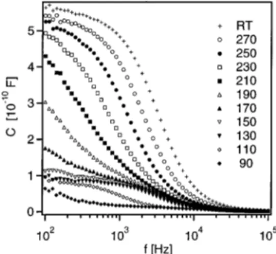
We show in Fig. 1, the (C – f ) curves for temperatures ranging from RT down to 90 K, for frequencies between 102 and 105Hz and for zero bias voltage. The C – f curves for the five highest temperatures show the same behavior. After a constant low-frequency capacitance value which is of 56 nF for RT conditions, the capacitance decreases down to a low value in the pF range. At RT, the cutoff frequency fcis of 3.5
kHz, it decreases when the temperature decreases. At 210 K, the shape of the C – f curves changes, leading for the lowest temperatures to a new plateau with a value of the capacitance
C around 8 nF, followed by a decreasing value of the
capaci-tance to which corresponds at 150 K a cutoff frequency of 4 kHz. When further decreasing the temperature, the cutoff frequency moves towards lower frequency values.
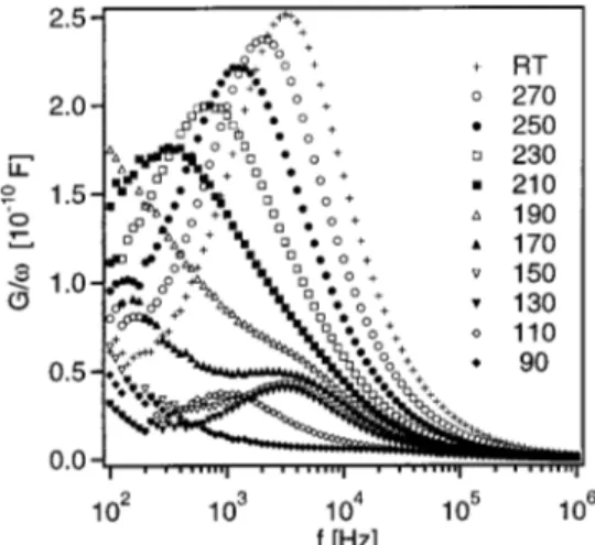
In Fig. 2, we show the results for the conductance G divided by⫽2f , where f is the measurement frequency.
For the five highest temperatures the G/ curves show a large peak centered at the cutoff frequencies of the previ-ously shown C – f curves. The amplitude of this peak de-creases with decreasing temperature. Below 230 K, a
shoul-FIG. 1. Experimental (C – f ) curves for temperatures T 共K兲 between RT and 90 K are shown. Steady-state applied voltage is V0⫽0 V.
der appears progressively on the high-frequency side of the
G/response. The shoulder leads to a distinct peak for peratures below 170 K. It is centered around 4 kHz for tem-peratures around 130 K, moving progressively to lower fre-quencies, when the temperature decreases.
At this stage, it would be tempting to directly use the peak positions fcof the G/curves for the 200 K–RT tem-perature range to deduce the acceptor activation energy from an Arrhenius plot. As the theoretical analysis will show, a linear correlation of fc/T2 as function of the inverse tem-perature 1/T may be accidental and does not return the input value of the activation energy. Due to its relatively large activation energy, Mg acts simultaneously as a dopant and deep impurity. This complex behavior has to be introduced in the theoretical analysis, as it may lead to a competition be-tween these two functions, the resulting characteristics de-pending on temperature and frequency.
Furthermore, the appearance of the low-temperature peak and its temperature dependence require the existence of a complementary mechanism, the Mg-related acceptor level determines the electrical characteristics above 200 K but can-not be related to the low-temperature results. Our interpreta-tion will show that the introducinterpreta-tion of a second acceptor level with an activation energy of several tens of meV can effectively explain the low-temperature admittance results.
III. THEORETICAL ANALYSIS A. Bulk carrier concentrations
To completely describe the system, one needs the param-eters corresponding to the semiconducting material, the junc-tions, and the fixed experimental conditions. GaN is a semi-conductor whose direct gap is 3.45 eV at RT. Magnesium is known as an acceptor, with however a relatively large ion-ization energy, whose value in the literature is mostly given at energies of 100 to 250 meV above the valence band edge
EV. This energy position will be labeled EtA and the
corre-sponding total concentration NtA. As suggested by the
ex-perimental characteristics at low temperatures, a second ac-ceptor state could be present. It will be taken into account in
the numerical analysis with its corresponding energy position
EtBand concentration NtB. The occupied level A concentra-tion is given by
ntA⫽
NtA
1⫹g exp关共EtA⫺EF兲/kT兴, 共1兲
where EFis the thermal equilibrium Fermi energy, and g the
degeneracy factor taken equal to 4. A similar expression holds for the occupied level B concentration ntB. The
ther-mal equilibrium hole concentration p depends on tempera-ture T according to
p⫽NVexp关共EV⫺EF兲/kT兴, 共2兲
where NV is the effective valence band density of states. The
electron concentration n expresses similarly. The charge neu-trality condition is written, including eventually present fully ionized donor and acceptor concentrations ND and NA,
p⫺n⫹ND⫺NA⫺ntA⫺ntB⫽0. 共3兲
From this relation, the equilibrium Fermi energy EF can
be obtained numerically. As an application, we show results for (EtA⫺EV)⫽210 meV, (EtB⫺EV)⫽30 meV, NtA⫽1
⫻1019cm⫺3, N
tB⫽2⫻1016cm⫺3, NA⫽ND⫽0. In Fig. 3, we
show as a function of temperature T, the resulting position of the Fermi energy EF, the hole concentration p, and the
oc-cupied level concentrations ntA and ntB. The position of the Fermi energy EF increases with increasing temperature T, keeping a position intermediate between the two defect en-ergies EtA and EtB. The carrier concentrations ntA and ntB vary accordingly, with a resulting value of ntB nearly con-stant above 160 K, close to NtB. For these temperatures, the
level B behaves as a shallow dopant, when it is considered as fully ionized. The resulting hole concentration is the sum of the contributions provided by the two acceptor levels. Below 140 K, it is essentially the shallowest level B which contrib-utes to the hole concentration and above 200 K, the contri-bution of the level A is the dominant one, due to its larger
FIG. 2. Experimental curves of conductance G divided by⫽2f as
func-tion of frequency f for temperatures T共K兲 between RT and 90 K are shown. Steady-state applied voltage is V0⫽0 V.
FIG. 3. Position of bulk thermal equilibrium Fermi energy EFwith respect
to the valence band edge EV, thermal equilibrium values of the hole
con-centration p, the level A occupation ntAand the level B occupation ntBas
function of temperature are shown. The total concentrations of the levels are, respectively, NtA⫽1⫻1019and NtB⫽2⫻1016cm⫺3and their energies
relative to the valence band edge are EtA⫽210 and EtB⫽30 meV. The inset
B. Basic equations and numerical procedure
The structure on which the measurements have been per-formed corresponds to a pair of Schottky diodes connected back to back with the GaN layer as a conducting channel. This complete system is treated in the theoretical analysis based on the resolution of the classical semiconductor equa-tions for the free carrier and occupied level concentraequa-tions. For the acceptor concentrations considered here and due to the large value of the gap of GaN, the electron concentration
n is several orders of magnitude smaller than the other
con-centrations and its contribution in the various equations can be neglected. The basic equations involve as unknowns the electrical potential, the hole concentration p, and the level concentrations ntA and ntB. In the numerical study, the sys-tem is considered as one-dimensional, with x giving the po-sition. The first equation is Poisson’s equation
“•共⑀“兲⫽⫺q 共p⫹ND⫺NA⫺ntA⫺ntB兲, 共4兲
where ⑀ is the dielectric constant and ⫺q the electronic charge. The continuity equation for the holes reads
p t ⫽⫺
1
q “•Jp⫺rptA⫺rptB. 共5兲
Here Jp is the hole current density, which is the sum of the
drift and diffusion terms
Jp⫽pp“EV⫺pkT“p, 共6兲
wherep is the hole mobility. The terms rptA and rptB rep-resent the electron transition rates between the levels A and B and the valence band. According to the Shockley–Read– Hall scheme22 these transition rates are written, for the case of level A
rptA共EtA兲⫽cpAp ntA⫺epA共NtA⫺ntA兲, 共7兲
where cpA is the capture rate for holes, expressed in terms of
the hole thermal velocity vth
p
and the hole thermal capture cross sectionpA by
cpA⫽vth
p
pA. 共8兲
The thermal emission rate epA is given by epA⫽
cpA
g NVexp关共EV⫺EtA兲/kT兴. 共9兲
Similar expressions hold for the transition rates to level B. The continuity equations for the occupied concentrations of levels A and B are, respectively
harmonic component whose amplitude, labeled with a tilde, is complex in the general case. For example, the hole con-centration writes
p共x,t兲⫽p0共x兲⫹p˜共x兲eit. 共12兲
Explicit expressions for the detailed developments are given in Refs. 23 and 24. The position of the left-hand side and right-hand side boundaries of the region occupied by the semiconducting material are, respectively, xL and xR.
We place the Schottky contacts at x⫽xLand xR. In the
boundary conditions, the Schottky barrier height qb is
fixed. In thermal equilibrium, it is related to the built-in po-tential Vbiand the bulk separation between the Fermi energy
EF and the valence band edge EV by25
qb⫽qVbi⫹共EF⫺EV兲. 共13兲
In addition, a finite surface recombination velocity has to be given to fully characterize the metal–semiconductor contact.26
Instead of using the variables, n, p, and nt, the equa-tions are expressed in terms of and the quasi-Fermi ener-gies Fp, FtA and FtB, as these are more appropriate, giving variations of the same order of magnitude for the four un-knowns. The set of Eqs.共4兲–共10兲 is then solved numerically, after scaling and discretization according to a variable size mesh. As results, one obtains the steady-state and small-signal values of the electrical potential, the concentrations
p, ntA, ntB, the recombination rates rptA and rptB, the
cur-rent density Jp, and the displacement current JD, in the ac
case. The total ac current density J˜ is constant with respect to
x. From its value, one obtains the admittance Y⫽J˜/V˜, from
which the total capacitance C and conductance G can be obtained
Y⫽G⫹iC. 共14兲
In this expression G an C are the equivalent parallel capaci-tance and conduccapaci-tance of the whole structure. Both G and C depend on the frequency f , the steady-state voltage V0, and the temperature T.
C. Microscopic description of the junction
Various results will be given in order to illustrate in the steady-state and small-signal case, typical space- and frequency-dependent basic features. They correspond to the aforementioned parameters for the acceptor level energies and their concentrations. In addition, the thermal capture
cross sections for both levels have been fixed at 2 ⫻10⫺19cm2. The hole mobility
p is fixed at 10 cm2/V s
above T0⫽150 K, and given a (T/T0)␣ dependence below that temperature. A decrease of the hole mobility below 150 K has effectively been observed experimentally.5–9The ex-ponent␣is considered as an additional parameter. In case of a temperature dependence imposed by impurity scattering, it is often given with a value of the order of 3/2. The Schottky barrier height is taken 1.05 eV and the surface recombination velocity of the holes is 109cm/s. It is assumed that both contacts are identical i.e., they have the same Schottky bar-rier height. In order to reproduce the electrical characteristics of the whole structure, one has to take into account the three-dimensional character of the real structure. The major diffi-culty results from the fact that the conduction channel be-tween the two contacts is not of a constant section. Its maximum value is at the Schottky contact whose diameter is in the millimeter range. The conduction between the contacts is through the GaN layer, whose thickness is in the microme-ter range. A way to adapt the one-dimensional numerical procedure to model this feature, is to introduce a multiplying factor Rfor the carrier mobilities in the region between the two depletion regions. This factor R, less than one, is of the order of the ratio between the GaN layer thickness and the contact diameter. A value of the order of R⫽0.005 can be expected. For the value of the resistance of the GaN layer, it is effectively equivalent to reduce the section of the conduc-tion channel or to reduce the conductivity by artificially re-ducing the hole mobility. As will be shown, this procedure reproduces the experimental values of the series resistance of the junction.
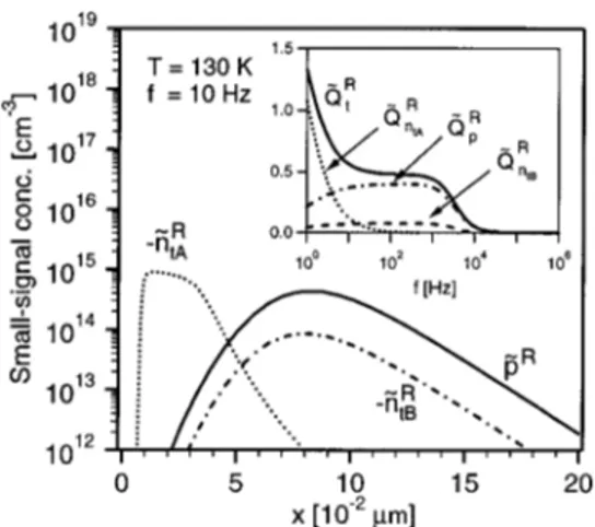
In Fig. 4, we show the small-signal values of the hole concentration p(x) and of the occupied level A concentration
ntA(x), near the left-hand side contact, for T⫽230 K, V0 ⫽0 V, and f ⫽10 Hz. The real part of the ac amplitude of ntA, i.e., n˜tA
R
, has its maximum at xA⫽0.01m, whereas p˜R
presents its maximum at xp⫽0.03m. The amplitude of the
variations of the shallow defect n˜tBR is much less important, at least with the chosen parameter set, therefore the related curve is not shown in Fig. 4. The same quantities are repro-duced in Fig. 5 for the low-temperature case T⫽130 K. Two major differences occur as compared to the T⫽230 K results. The amplitude of n˜tAR is considerably reduced, while that of the modulated hole concentration p˜R has increased and is now the leading term in the ac response. These are conse-quences of the temperature dependence of the bulk Fermi level position with respect to the valence band edge and of the resulting junction energy band diagram.
All quantities shown up to now depend on the external parameters temperature and frequency. In order to give a synthesis of the frequency dependence, we show in the inset of Fig. 4, for T⫽230 K and V0⫽0 V, as a function of fre-quency, the integrated real part of the ac amplitudes of p,
ntA, ntB, and of the charge density. The different parts are defined as follows Q˜ntA R ⫽q
冕
xL xu 共⫺n˜tA R兲dx, 共15兲 Q˜n tB R ⫽q冕
xL xu 共⫺n˜tB R兲dx, 共16兲 Q˜pR⫽q冕
xL xu p ˜Rdx, 共17兲 Q˜tR⫽q冕
xL xu 共p˜R⫺n˜ tA R⫺n˜ tB R 兲dx, 共18兲where xu is an upper limit of integration, sufficiently large such that the different integrands can be considered as zero beyond xu. The charge defined by relation共18兲 relates to the
imaginary part of the total current amplitude by
J ˜I⫽Q˜
t
R. 共19兲
FIG. 4. Real part of small-signal amplitudes at the left contact (x⫽0) for hole concentration p, occupied level A concentration ntA, at temperature T⫽230 K, and for frequency f ⫽10 Hz are shown. The small-signal
ampli-tude of occupied level B concentration is too low to appear in this plot. Inset: Integrated modulated charge per unit section共in 10⫺9C/cm2兲 as
func-tion of frequency f , due to hole concentrafunc-tion p, level A, level B共nearly zero兲, and total charge density, at T⫽230 K and zero steady-state applied voltage.
FIG. 5. Real part of small-signal amplitudes at the left-hand side contact (x⫽0) for hole concentration p, occupied level A concentration ntA,
occu-pied level B concentration ntB, at temperature T⫽130 K and for frequency f⫽10 Hz are shown. Inset: Integrated modulated charge per unit section 共in
10⫺9C/cm2兲 as function of frequency f , due to hole concentration p, level
A, level B, and total charge density, at T⫽130 K and zero steady-state applied voltage.
Q˜tR by the voltage amplitude V˜ yields the frequency-dependent capacitance of the single junction, as a result from relations 共14兲 and 共19兲. In fact, this is a case where the
RsC-cutoff frequency, with Rs as the series resistance and C
as the hole depletion layer capacitance is located slightly above the defect-A transition frequency ftA. Therefore, the
hole response cannot reach its maximum amplitude and the total cutoff frequency is practically equal to the defect tran-sition frequency ftA.24
In the inset of Fig. 5 we show the same quantities, but for a low-temperature case, with T⫽130 K. The response of the level A has moved to lower frequencies, by about 3 de-cades. The hole amplitude modulation is maximum for f ⫽3⫻102Hz. The resulting amplitude of the integrated charge density modulation shows now a two-step behavior with a low-frequency cutoff determined by the level A re-sponse and a second cutoff above 103Hz determined by the hole response. In terms of equivalent electrical circuits, the hole response is due to the modulation of the depletion layer width, whose cutoff frequency is given, in the case of a clas-sical junction with fully ionized shallow dopants by the RsC
constant of the structure, where Rs is the series resistance
and C is the depletion layer capacitance.
D. Admittance curves of the back to back connected Schottky junctions
The theoretical curves are obtained with a one-dimensional system giving electrical quantities per unit sec-tion. In the following, the section will be fixed by normal-ization of the low-frequency value of the RT capacitance to the experimental RT capacitance value. Normalizing to the height of the main peak in the G()/ curve would yield similar results. To analyze the resulting electrical character-istics, a series of parameters describing the structure has to be fixed. The length (xR⫺xL) is taken equal to the mean distance between the two contacts. The hole effective mass is fixed at mp⫽0.8m0.5 The parameters which remain to be determined are the Schottky barrier height qb at the two
junctions, the position of the two levels EtAand EtBand their
respective concentrations NtAand NtB, their thermal capture
cross sectionspA andpB and the factor R. The RT hole
mobilty p has been fixed to 10 cm2/V s, with a (T/T0)␣ temperature dependence below T0⫽150 K. We have not considered the mobility p as an independent parameter as
the reduction factor R is already used. The concentrations
of eventually present, other completely ionized shallow do-nors, ND, and acceptors, NA, have been set equal to zero.
The electrical characteristics are then calculated at vari-ous temperatures, starting from an initial guess with typical values as given in the literature. In the optimization proce-dure, a least-square fit is used to determine the open param-eters such as to best reproduce the experimentally obtained
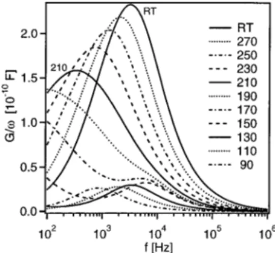
G/ curves. In a first step, the major features such as the peak positions are adjusted, a refinement in a second step corrects the complete set of temperature-dependent G/ curves. Figure 6 gives the resulting C – f curves and Fig. 7, the G/ curves. The obtained parameters are R⫽0.007,
␣⫽3, qb⫽1.05 eV, (EtA⫺EV)⫽210 meV, (EtB⫺EV)
⫽30 meV, NtA⫽1⫻1019cm⫺3, NtB⫽2⫻1016cm⫺3, pA
⫽2⫻10⫺19cm2, and
pB⫽2⫻10⫺19cm2.
First, the as-obtained parameters are compared to experi-mental values reported in the literature. Schottky barrier heights depend on the nature of the metal, on surface prepa-ration conditions, and on interface oxide layers. For contacts on p-doped GaN, barrier heights are obtained from an analy-sis of I – V characteristics and give, respectively, qb
⫽0.9 eV,271.05 eV,190.50–0.65 eV,150.49 eV,17even values
FIG. 6. Theoretical C – f curves for temperatures between RT and T
⫽90 K are shown. Steady-state applied voltage is V0⫽0 V.
FIG. 7. Theoretical G/curves as a function of frequency for temperatures between RT and T⫽90 K are shown. Steady-state applied voltage is V0 ⫽0 V.
as high as 2.4 eV for Ni/p-GaN contacts have been mentioned.28The activation energy of the Mg-related accep-tor level has been determined by various methods, the result-ing values depend on growth method and Mg concentration. From the study of the temperature dependence of the hole concentration obtained by Hall measurements on GaN lay-ers, values of 112 to 190 meV are given,4 –9by admittance spectroscopy, values of 70 to 160 meV are cited.2– 4In some cases, the value obtained by admittance measurements was lower than that obtained from the Hall method.4 Photolumi-nescence studies of the donor–acceptor recombination yield again a different set of values between 150 and 250 meV.10–14The thermal capture cross section of the A level of 2⫻10⫺19cm2is close to the value given by admittance spec-troscopy in Ref. 4.
Several acceptor levels in the same sample have been observed experimentally.2,5,29Their energy positions depend on the growth method and sample preparation, but most are located at least at 100 meV above the valence band edge. In our study, their concentration NtBis rather weak as compared
to the value of NtA, and their effect only appears at
tempera-tures below 150 K. This may explain why acceptor levels with activation energies around 30 meV have not been de-tected in the past with the used experimental techniques. The thermal capture cross section for level B has been set equal to that for the level A. As will be seen from the discussion below, it is not possible to determinepBfrom the electrical characteristics, as the level B influences the thermal equilib-rium Fermi energy and the temperature-dependent hole con-centration, but not the dynamical response to the applied modulating voltage.
The theoretically obtained temperature-dependent C – f and G/ curves well reproduce the experimental curves shown in Figs. 1 and 2. The different regimes at high and low temperatures can be explained with the help of the above mentioned microscopic characteristics.
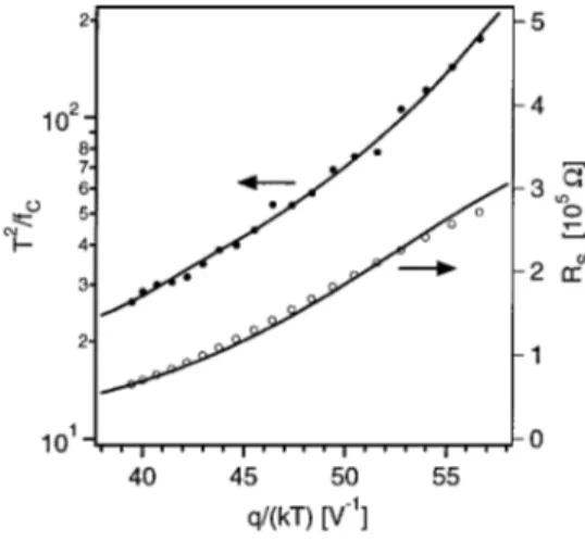
Above 200 K, the capacitance is due to the modulation of the space charge for which the defect state A related to the magnesium is responsible. Figure 8 gives the experimental
and theoretical value of T2/ fc, where fcis the peak position
of G/ in this temperature range. Good agreement between theory and experiment is obtained. The figure also shows a comparison of the experimental and theoretical value of the equivalent series resistance, which is obtained from the high-frequency value of the real part of the impedance Z⫽1/Y. At high frequency, the equivalent circuit of the whole structure reduces to the series resistance Rs as the impedance of the
capacitances becomes negligible. The agreement between the experimental and theoretical values justifies the use of the reduction factor R, to simulate the effect of the geometrical structure. In Fig. 9, we show for RT conditions, the theoreti-cally obtained value of the position of the dominant peak in the G/ curves fcas a function of the reduction factor R,
for values of R between 0.001 and 1. For values of R above 0.4, the peak frequency remains constant, as it corre-sponds to the defect transition frequency. A second peak in the G/curves is at a higher frequency and corresponds to a
RC cutoff. Below R⫽0.4, it progressively merges into the
first peak, leading to a slight increase on the resulting peak frequency. Below R⫽0.1, the peak frequency decreases. As the inset of Fig. 9 shows, the variation of fcis nearly linear
in that parameter range. The frequency fc is proportional to R, i.e., inversely proportional to the series resistance Rs.
This strongly indicates that the RT temperature cutoff fre-quency is due in fact to the electrically RsC cutoff, where C
is the low-frequency capacitance, and no more to the defect transition frequency.
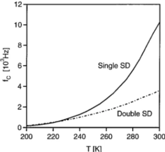
An additional argument in favor of this interpretation in this temperature range is furthermore given by the results shown in Fig. 10, where the cutoff frequency position fc is shown as function of temperature T. The lower curve gives the values of fc for the up to now studied double Schottky
structure, whereas the upper curve corresponds to a single Schottky diode with a total length of 1 m, and R⫽1. In this latter case, no RsC-cutoff frequency can be expected in
this temperature range, fc therefore is equal to the defect
transition frequency ftA. The comparison of the frequencies fcfor the two systems clearly shows the transition between
FIG. 8. Theoretical (⫺) and experimental (䊉) values of T2/ fc, with fcthe
capacitance cutoff frequency共equal to the G/peak position兲 as function of the inverse thermal voltage q/kT for temperatures from T⫽200 to T
⫽300 K. The second curve shows the theoretical (⫺) and experimental
(䊊) values of the series resistance Rs.
FIG. 9. Position of main peak in G/vs frequency curve at T⫽293 K, as function of the reduction factor R is shown. The inset shows same values in the enhanced region of R⫽0.001 to 0.015. Numerical fit yields best agreement for R⫽0.007.
the two regimes. Above 250 K, the electrical behavior of the circuit determines the cutoff frequency. Below 230 K, it is the reduced response of the Mg-related defect state EtA, which imposes the reduction of the equivalent capacitance of the structure.
As a consequence, care should been taken in attempting to directly deduce the activation energy from an Arrhenius plot. First, the system under study here consists of the Mg level, which acts simultaneously as the p dopant and deep impurity. This is a situation where the assumptions leading to the identification of the defect transition frequency ft with
the thermal emission rate are not fulfilled.18,24,30Even when resistance effects do not exist, this leads to an expression of
ftwhich is not simply equal to the hole emission rate ep, the
difference in magnitude being of the order of a factor 10–50 and the temperature dependence not simply that of a thermally-activated process. Starting with an input value of (EtA⫺EV)⫽210 meV, we have determined ftA by
calculat-ing the G/peak position for a single and sufficiently short Schottky diode, such that series resistance effects play no role. With temperatures from 200 to 300 K, the Arrhenius plot yields an activation energy of 176 meV. This apparent shift of 30– 40 meV corresponds to similar values as were obtained by Kozodoy et al.18and Kim.30Using the values of the theoretical peak positions for the complete structure as shown in Fig. 8, one obtains an apparent linear relation in a log representation of T2/ f
cas a function of the inverse
ther-mal voltage q/kT. The resulting activation energy is now 107 meV, which is clearly distinct from the input value 210 meV and the ideal transition frequency ftA⫽176 meV. As
this discussion has shown, the cutoff frequency is the feature resulting from two cutoff mechanisms which both are present in the 200–300 K temperature range. The fact of obtaining a linear relationship in a semilog representation might there-fore be, in some cases, purely fortuitous. It implicitly as-sumes that the temperature dependence of the transition fre-quency is the same as that of the thermal hole emission rate, as given by expression共9兲. But doing so even in the case of deep impurities, at concentrations lower than that of the
shal-modulation in the vicinity of the junctions are given. It is shown that the response of level A has moved to very low frequencies, below 10 Hz. The response of level B is nonzero but an order of magnitude lower than that of the holes. For this reason, it is impossible to get a precise quantitative in-formation on the capture cross section of this shallow accep-tor level. Above 10 Hz, the major contribution is due to the holes. This corresponds to the modulation of the depletion
layer width in a classical p-n junction or a
metal/ p –semiconductor junction. This contribution remains when the deep impurity levels no longer respond to the variations of the applied voltage. The cutoff frequency is equal to 1/(2RsC) where Rs is again the series resistance
essentially due to the conducting layer between the depletion layers and C is the combined capacitance of the two Schottky contacts. The capacitance of each contact is only weakly temperature-dependent in this temperature range, and the variation of the peak position and amplitude with tem-perature is mainly due to the temtem-perature dependence of the series resistance. The RC-cutoff frequency is therefore pro-portional to the conductivity of the GaN layer, which means proportional to the hole concentration p and the hole mobil-ityp. As seen in Fig. 3, the hole concentration p decreases
only weakly from 160 to 120 K, as does the mobility p,
which explains that the displacement of this peak, is small in this temperature range. Below 120 K, the reduction in tem-perature of the hole concentration p and of the hole mobility due to increased impurity scattering, is responsible for the lowering of the capacitance cutoff frequency and of the low-temperature peak position. The reduction of the peak height with temperature is due to the reduction of the effective hole concentration p. The appearance of this peak in the admit-tance curves is the combined result of the large value of the series resistance, the large distance between the contacts, the low intrinsic hole mobility of GaN and the geometry of the double Schottky structure, which is included through the re-duction factor R. As shown in Fig. 7, this second peak does not appear in the high-temperature curves as it is hidden by the high-frequency part of the first peak.
We have attempted to explain the existence and tempera-ture dependence of this low-temperatempera-ture peak by other ef-fects, such as an asymmetry between the two contacts, a second level of donor type or a second acceptor level being fully ionized at all temperatures, which is equivalent to a nonzero concentration NA. But all these models were
un-able to correctly reproduce the experimental results. Taking, for example, a constant value of NA produces a
low-FIG. 10. Position of main peak in G/vs frequency curve as function of temperature T, for complete double Schottky diode structure共lower curve兲 and for single Schottky contact with reduced length (xR⫺xL)⫽1m, R ⫽1 and otherwise identical parameter set 共upper curve兲.
temperature peak in the G/ curves by the same RC-cutoff mechanism, but there is only a weak shift of this peak when the temperature decreases. This final analysis shows that only the introduction of a second acceptor state with an ac-tivation energy of about 30 meV completely explains the low-temperature electrical characteristics.
IV. CONCLUSIONS
We have determined experimental temperature-dependent admittance curves for Mg-doped GaN double Schottky diodes grown by MOCVD. The G/ curves show in the temperature range of T⫽200– 300 K a dominant peak which moves to lower frequencies with decreasing tempera-ture. The capacitance–frequency curves have cutoff frequen-cies at the same values. Below 150 K, a second peak in the
G/ curves appears with its own temperature dependence. The theoretical study is based on the numerical simula-tion of the complete structure with the two Schottky contacts and the hole conduction through the GaN channel between the contacts. It includes the Mg-related acceptor level at an energy position of 210 meV above the valence band edge
EV, with a total concentration of NtA⫽1⫻1019cm⫺3, as
well as a second shallow acceptor state at 30 meV above EV
and a concentration of 2⫻1016cm⫺3. The numerical results explain the basic mechanisms responsible for the tempera-ture dependence of the ac electrical characteristics, leading to a good agreement with the experimentally obtained values.
The analysis suggests that only a complete numerical study allows a correct interpretation of the admittance curves. In particular, the microscopic parameters can only be obtained from an optimized fit with a numerical simulation program. It is explicitly shown that deducing activation en-ergies from an Arrhenius plot of the transition frequencies would lead in the case of the system we have studied to an underestimation of the activation energies.
This work contributes to the basic understanding of the role played by the particular dopant which is magnesium, having the functions of dopant and deep impurity simulta-neously. Which role is dominant depends on the external conditions such as temperature, applied voltage or modula-tion frequency, and on the characteristic values of the Mg acceptor itself, mainly its energy position in the gap and its concentration. Despite the numerous works devoted to this system, many aspects remain to be explored.
The experimental aspects could be completed by studies under modified experimental conditions, such as illumination or large-signal response and by using structures which re-duce to a single metal–semiconductor contact where series resistance effects could be neglected. There, only the intrin-sic response of the Mg-level would contribute to the electri-cal signal. The numerielectri-cal study could of course be applied to other configurations of interest, such as GaN-based transis-tors, photodetectransis-tors, and p-n junctions. The latter are the
basis of LEDs. Inclusion of more than two acceptor levels, as well as donor levels in the forbidden gap or a continuous defect density of states, are also possible.
ACKNOWLEDGMENTS
Financial support by the Belgian Fonds National de la Recherche Scientifique共Contract No. 9.4565.96F兲 and by an INTAS Grant No. N97-0995 are gratefully acknowledged.
1S. J. Pearton, J. C. Zolper, R. J. Shul, and F. Ren, J. Appl. Phys. 86, 1 共1999兲.
2J. W. Huang, T. F. Kuech, H. Lu, and I. Bhat, Appl. Phys. Lett. 68, 2392 共1996兲.
3Y. Zohta, H. Kuroda, R. Nii, and S. Nakamura, J. Cryst. Growth 189, 816 共1998兲.
4D. J. Kim, D. Y. Ryu, N. A. Bojarczuk, J. Karasinski, S. Guha, S. H. Lee, and J. H. Lee, J. Appl. Phys. 88, 2564共2000兲.
5
T. Tanaka, A. Watanabe, H. Amano, Y. Kobayashi, I. Akasaki, S. Yamazaki, and M. Koike, Appl. Phys. Lett. 65, 593共1994兲.
6W. Go¨tz, N. M. Johnson, J. Walker, D. P. Bour, and R. A. Street, Appl. Phys. Lett. 68, 667共1996兲.
7
H. Nakayama, P. Hacke, M. R. H. Khan, T. Detchprohm, K. Hiramatsu, and N. Sawaki, Jpn. J. Appl. Phys., Part 2 35, L282共1996兲.
8H. Nagai, Q. S. Zhu, Y. Kawaguchi, K. Hiramatsu, and N. Sawaki, Appl. Phys. Lett. 73, 2024共1998兲.
9
P. Kozodoy, H. Xing, S. P. Den Baars, U. K. Mishra, A. Saxler, R. Perrin, S. Elhamri, and W. C. Mitchel, J. Appl. Phys. 87, 1832共2000兲. 10M. Ilegems and R. Dingle, J. Appl. Phys. 44, 4234共1973兲. 11J. A. Pankove and J. A. Hutchby, J. Appl. Phys. 42, 5387共1976兲. 12U. Kaufmann, M. Kunzer, M. Maier, H. Obloh, A. Ramakrishnan, B.
Santic, and P. Schlotter, Appl. Phys. Lett. 72, 1326共1998兲.
13T. W. Kang, S. H. Park, H. Song, T. W. Kim, G. S. Yoon, and C. O. Kim, J. Appl. Phys. 84, 2082共1998兲.
14A. K. Viswanath, E. Shin, J. I. Lee, S. Yu, D. Kim, B. Kim, Y. Choi, and C. H. Hong, J. Appl. Phys. 83, 2272共1998兲.
15
T. Mori, T. Kozawa, T. Ohwaki, Y. Taga, S. Nagai, S. Yamasaki, S. Asami, N. Shibata, and M. Koike, Appl. Phys. Lett. 69, 3537共1996兲.
16A. Krtschil, H. Witte, M. Lisker, J. Christen, U. Birkle, S. Einfeldt, and D. Hommel, J. Appl. Phys. 84, 2040共1998兲.
17
X. A. Cao, S. J. Pearton, G. Dang, A. P. Zhang, F. Ren, and J. M. Van Hove, Appl. Phys. Lett. 75, 4130共1999兲.
18P. Kozodoy, S. P. Den Baars, and U. K. Mishra, J. Appl. Phys. 87, 770 共2000兲.
19E. Monroy, F. Calle, J. L. Pau, F. J. Sanchez, E. Munoz, F. Omnes, B. Beaumont, and P. Gibart, J. Appl. Phys. 88, 2081共2000兲.
20E. Monroy, M. Hamilton, D. Walker, P. Kung, F. J. Sanchez, and M. Razeghi, Appl. Phys. Lett. 74, 1171共1999兲.
21Z. M. Zhao, R. L. Jiang, P. Chen, D. J. Xi, Z. Y. Luo, R. Zhang, B. Shen, Z. Z. Chen, and Y. D. Zheng, Appl. Phys. Lett. 77, 444共2000兲. 22
W. Shockley and W. T. Read, Phys. Rev. 87, 835共1952兲; R. N. Hall, Phys. Rev. 87, 387共1952兲.
23M. Sakhaf and M. Schmeits, J. Appl. Phys. 80, 6839共1996兲.
24M. Schmeits, N. D. Nguyen, and M. Germain, J. Appl. Phys. 89, 1890 共2001兲.
25S. M. Sze, Physics of Semiconductor Devices共Wiley, New York, 1981兲. 26S. Selberherr, Analysis and Simulation of Semiconductor Devices
共Springer, Berlin, 1984兲. 27
Z. Z. Bandic, P. M. Bridger, E. C. Piquette, and T. C. McGill, Appl. Phys. Lett. 73, 3276共1998兲.
28K. Shiojima, T. Sugahara, and S. Sakai, Appl. Phys. Lett. 74, 1936共1999兲. 29H. Nagai, Q. S. Zhu, Y. Kawaguchi, K. Hiramatsu, and N. Sawaki, Appl.
Phys. Lett. 73, 2024共1998兲. 30
D. J. Kim, J. Appl. Phys. 88, 1929共2000兲.