HAL Id: hal-02932318
https://hal.archives-ouvertes.fr/hal-02932318
Submitted on 18 Dec 2020HAL is a multi-disciplinary open access archive for the deposit and dissemination of sci-entific research documents, whether they are pub-lished or not. The documents may come from teaching and research institutions in France or abroad, or from public or private research centers.
L’archive ouverte pluridisciplinaire HAL, est destinée au dépôt et à la diffusion de documents scientifiques de niveau recherche, publiés ou non, émanant des établissements d’enseignement et de recherche français ou étrangers, des laboratoires publics ou privés.
Control of stoichiometry and morphology in
polycrystalline V2O3 thin films using oxygen buffers
Jonathan Rupp, Benoît Corraze, Marie-Paule Besland, Laurent Cario, Julien
Tranchant, Dirk Wouters, Rainer Waser, Etienne Janod
To cite this version:
Jonathan Rupp, Benoît Corraze, Marie-Paule Besland, Laurent Cario, Julien Tranchant, et al.. Con-trol of stoichiometry and morphology in polycrystalline V2O3 thin films using oxygen buffers. Journal of Materials Science, Springer Verlag, 2020, 55 (30), pp.14717-14727. �10.1007/s10853-020-05028-0�. �hal-02932318�
Title:
Control of stoichiometry and morphology in polycrystalline V2O3 thin films using oxygen buffers
Authors:
J. A. J. Rupp1,*, B. Corraze3 , M.‐P. Besland3, L. Cario3, J. Tranchant3, D. J. Wouters1, R.
Waser1,2, E. Janod3
Affiliations:
1) RWTH Aachen (Germany)
Jonathan A. J. Rupp, rupp@iwe.RWTH‐Aachen.de *Corresponding Author
Dr. Dirk J. Wouters, wouters@iwe.RWTH‐Aachen.de Prof. Dr. Rainer Waser: waser@iwe.RWTH‐Aachen.de 2) PGI‐7 FZ Jülich (Germany) Prof. Dr. Rainer Waser: waser@iwe.RWTH‐Aachen.de 3) Institut des Matériaux Jean Rouxel (IMN) Université de Nantes, CNRS (France) Dr. Benoît Corraze : benoit.corraze@cnrs‐imn.fr Dr. Marie‐Paule Besland : marie‐paule.besland@cnrs‐imn.fr Dr. Etienne Janod : etienne.janod@cnrs‐imn.fr Dr. L. Cario : laurent.cario@cnrs‐imn.fr Dr. J. Tranchant : julien.tranchant@cnrs‐imn.fr Key words: Vanadium Sesquioxide, V2O3, Stoichiometry, Oxygen Buffer, Buffer Couple
Abstract:
In this work, we investigate the influence of low temperature reduction conditions (873 K) by
different oxygen buffers on the off‐stoichiometry of polycrystalline V2O3 thin films. Vanadium
oxide thin films (thickness 300 nm and 100 nm) have been grown by reactive sputtering and
have been annealed in a buffered atmosphere subsequently. Buffer couples were chosen
throughout the stability range of V2‐yO3 (y ≤ 0.03) by the use of different oxygen buffer
combinations, namely Ni/NiO, Fe/Fe3O4, Cr/Cr2O3 and Mn/MnO. Thin films have been
characterized by scanning electron microscopy, X‐ray diffractometry and low temperature
electrical transport measurements. Upon decreasing the oxygen partial pressure, the mean grain size of V2O3 decreases systematically from 45±20 nm with a high porosity to 27±10 nm without porosity. The most favourable reduction conditions have been identified for Fe‐ and Cr‐based couples. Moreover, all four buffer couples exhibit high transition temperatures of the IMT transition (110 ‐ 155 K) close to ideally stoichiometric V2O3 (y < 0.005) as well as large changes in resistance at the transition (three to five orders of magnitude). This oxygen buffer method hence provides a valuable synthesis method of highly stoichiometric polycrystalline V2O3 thin films with technological relevance. 1. Introduction: The binary system of vanadium and oxygen consists of various Magnéli VnO2n‐1‐ and Wadsley
VnO2n+1 phases [1]. Most of these phases show remarkable electronic and magnetic phase
transitions [2]. Amongst them, corundum‐type V2O3 undergoes an Insulator‐to‐Metal
transition (IMT) at 155 K. This transition occurs between an antiferromagnetic (insulating)
monoclinic phase at low temperature and a paramagnetic (conducting) rhombohedral
accompanied by a drop of the c/a ratio as well as an increase in volume of about 1.2 % [4]. At
room temperature, substituting vanadium with more than 1.1 at. % chromium induces a transition from paramagnetic metal to paramagnetic Mott insulator while retaining the same corundum structure. Applying physical pressure on (V1‐xCrx)2O3 leads to the inverse IMT and restores the metallic state. More interestingly, the Mott insulator‐to‐metal transition can not only be driven by pressure or temperature [4] but also by an electric field [5]. Therefore, this archetype Mott‐Hubbard‐insulator is of strong interest for application in resistively switching devices [6] and neuromorphic circuits [7][8]. However, very accurate control of stoichiometry
is required to achieve a well‐defined Mott‐insulating state that matches the required half‐
filling criteria [9]. Such a control of the vanadium‐oxygen ratio is crucial in thin films on which
further electrical applications will be based. For instance, deviations of stoichiometry in V2‐yO3
as low as y = 0.03 indeed lead to an absence of the low temperature IMT [10]. To reach low
oxygen content compounds under thermodynamic control, reduction experiments can be
performed in reducing atmospheres such as CO/CO2 or Ar/H2 [11], usually at high
temperatures above 1000 K. For instance, Shivashankar et al. investigated the controlled
formation of non‐stoichiometric V2‐yO3 across the pure‐phase window at a reduction
temperature of 1473 K in CO/CO2 atmosphere with subsequent quenching [10]. A huge
reduction of the vanadium point defect density (decreasing y from 0.02 down to 0.007) with
a concomitant increase of transition temperature from 10 K to 155 K could be achieved by
lowering the oxygen partial pressure towards the equilibrium line of VO/V2O3. An alternative
method to control the oxygen partial pressure can be achieved by an oxygen buffer method
[12] that similarly imposes an oxygen partial pressure with a metal – metal oxide buffer couple
(see experimental part). Here we show that reduction with an oxygen buffer can be
annealing temperatures such as 873 K. Four different buffer couples (BC) have been chosen
to aim at four different stoichiometry values in the range of phase‐pure V2O3. Based on
thermochemical data [13], one might expect that the vanadium vacancies y in V2‐yO3 decreases with the BC’s according to yNi NiO > yFe‐Fe3O4 > yCr‐Cr2O3 > yMn‐MnO. On the contrary, we found that for thin films, reduction annealing with the mentioned oxygen buffers does not follow the thermodynamic principle of single crystals reduced at high temperatures anymore. 2. Experimental: One promising way to succeed a very precise control of oxygen point defects is to exploit the condition of thermodynamic equilibrium for metal‐oxide reactions. Each dynamic equilibrium between a metal and a corresponding oxide is defined by its Gibbs free energy ∆𝐺 that consists
of an enthalpy 𝛥𝐻 and entropy 𝛥𝑆 terms. In this case, referring to the Ellingham
approximation, both are considered temperature‐independent. The change in ∆𝐺 can then be
related to the oxygen partial pressure 𝑝 O in a direct way :
∆𝐺 𝛥𝐻 𝑇𝛥𝑆 R𝑇 ln 𝑝 O (1) where R denotes the gas constant, 𝑇 the temperature and 𝑝 O the oxygen partial pressure
in thermodynamic equilibrium between the two solids. With given reaction enthalpies and
entropies from literature (Table 1), the equilibrium oxygen partial pressure was
straightforwardly calculated for four different oxygen buffer associations within the window
of off‐stoichiometric V2O3. Amorphous vanadium oxide thin films (thickness 300 nm and
100 nm) have been deposited on silica by RF‐reactive sputtering from a one inch vanadium
target. The oxygen partial pressure p(O2) was adjusted by the flux ratio of two mass flow
controllers: one with pure argon (90 sccm) and one with a mixture of argon and oxygen in the
low oxygen partial pressure value of 10 nbar was used to reach a V:O ratio close to 2:3 in the
amorphous films prior to reducing annealing (where the measured average value constituted
2:4[14]). The used power of P = 50 W and the process pressure of p = 10 µbar resulted in a
deposition rate of q = 3.3 nm/min. Thin films were subsequently placed inside silica tubes with
a metal and oxide powder couple at a pressure of p < 10‐3 mbar to provide a constant V:O
stoichiometry ratio independent of temperature. After sealing, the tubes were annealed in a
tubular furnace at a temperature of 873 K, with a heating rate of 300 K / h, an annealing time
of 1h at 873 K, and finally passive free cooling down to room temperature with a rate of
~100 K / h. Figure 1 displays the theoretical equilibrium oxygen partial pressures for the four
selected buffer couple reactions between metals and oxides with respect to temperature.
Buffer couples were chosen to introduce an increasing concentration of vanadium defects as
a result of an increase of oxygen partial pressure from Mn‐ based to Cr‐/Fe‐/Ni‐based BCs.
Metal and oxide quantities were weighted according to the reaction equation’s mole masses.
Morphology was determined by scanning electron microscopy (SEM) images with a Zeiss
“DSM982 GEMINI” microscope. Lateral grain sizes were determined by the line section
method. Surface vacancy area (100 nm layers) and surface crack area (300 nm layers) were
determined by ImageJ 1.51d with a contrast filter. X‐ray diffraction (XRD) patterns were
recorded in Bragg‐Brentano geometry with a Bruker X‐Ray diffractometer. Lattice parameters
were extracted by le Bail refinement with JANA software from X‐ray diffraction (XRD)
patterns. To investigate electrical transport characteristics at low temperatures in four‐point
configuration, a closed‐cycle helium circuit cryostat “Omniplex DE210” from ARS was used.
Transition temperatures of the IMT were determined for the cooling and heating branch at
the turning point of the derivative logarithmic resistance versus inverse temperature
3. Results:
3.1 Morphology
Figure 2 shows morphological changes of V2O3 thin films throughout the stoichiometry
window. As‐deposited amorphous 100 nm thick films already present a rough surface with
relatively large particles up to 36 nm in diameter (Figure 2a1&2) whereas 300 nm thick films
show a relatively dense columnar structure (Figure 2a3&4). The 100 nm thick film annealed
with BC Ni/NiO exhibits a grain size of dNi,100 = 39±14 nm with visible surface pinholes
(Figure 2b1&2). The grain size is comparable to the pristine amorphous state (Figure 2a1&2).
For a higher thickness of 300 nm (Figure 2b3&4), grain size increases slightly
(dNi,300 = 44±18 nm) compared to 100 nm thick thin films and the cross section image shows a
more porous bulk morphology as compared to the pristine amorphous dense columnar
structure (Figure 2a3&4). For BC Fe/Fe3O4 (Figure 2c1&2) and a thickness of 100 nm, grain size
(dFe,100 = 23±7 nm) as well as pinhole size decreases compared to Ni/NiO, quantitatively
described by Figure 2f&g. With respect to the 100 nm films reduced by Fe/Fe3O4, an increased
grain size is obtained for 300 nm (dFe,300 = 36±15 nm) thick layers (Figure 2c3&4). In addition,
a considerable part of the surface is covered with formed cracks (Figure 2c3). Layers
synthesized with a BC Cr/Cr2O3 (Figure 2d1&2) show a smaller average grain size
(dCr,100 = 20±8 nm) with few smaller pinholes for 100 nm layers as compared to 100 nm thick
layers annealed with BC Fe/Fe3O4 (Figure 2c1&2). Corresponding 300 nm thick layers
(Figure 2d3&4) still form cracks to a lesser extent compared to BC Fe/Fe3O4 (Figure 2c3&4)
and present only a slightly higher grain size than 100 nm layers (dCr,300 = 23±7 nm). Lastly, BC
considerably higher roughness compared to BC Cr/Cr2O3 which is reflected by a spatial
variation in contrast. For 300 nm layers (Figure 2e3&4), a flatter surface with increased grain
size is visible compared to 100 nm thin films (dMn,300 = 26±10 nm). Yet, in this case, broad hills
grow on the surface (instead of cracks as found for BCs Fe/Fe3O4 and Cr/Cr2O3). To sum up,
grain sizes (Figure 2f) and free volume (Figure 2g) decreases equally with the sequence of
buffer couples for both thicknesses.
3.2 Crystal Structure and Lattice Parameters
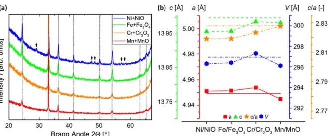
All films were characterized by XRD analysis. XRD records from 100 nm thick films exhibit
diffraction peaks with weak intensity, not suitable to accurately resolve lattice parameters. Thus, cell parameters were extracted from XRD patterns obtained for 300 nm thick V2O3 thin films (Figure 3a). For the V2O3 thin film obtained by buffer couple Ni‐NiO, black arrows denote an (unknown) formed secondary phase. Table 2 summarizes the obtained lattice parameter values and fitting parameters. In Figure 3b, the variation of unit cell parameters as function of BC type is plotted (where bulk V2O3 values are indicated by horizontal lines). For all buffer couples, the c/a ratios (orange star) deviate from the bulk value except for Mn/MnO where
the c/a ratio matches the ideal c/a ratio of V2O3. Furthermore, with BC Ni/NiO for off‐
stoichiometric V2‐yO3, c parameter (green triangle) and cell volume (blue hexagon) are
compressed by 0.05 Å and 1 Å3, respectively, whereas the a parameter (red square) is slightly expanded by 0.01 Å. With BC to lower p(O2) (left to right in Figure 3b), c‐parameter and cell volume relax to bulk values whereas the a‐parameter expands even more up to the BC Cr‐ Cr2O3. For BC Mn/MnO, parameters a and c as well as the cell volume are reduced compared to bulk.
3.3 Electrical Transport Characteristics
With low temperature electrical transport measurements, the insulator‐to‐metal transition of
V2O3 was investigated for 300 nm thick films (Figure 4a) as well as 100 nm thick films
(Figure 4b). For all buffer couple combinations, both thicknesses exhibit exactly the same
trends with sharp transition behaviour as well as an increase of room temperature resistivity
towards the equilibrium line of V2O3/VO, indicating a high reproducibility of the reduction
process in this thickness range. The lowest transition temperatures between 90 K and 140 K
were found for the two extreme BC’s, namely Mn‐MnO and Ni‐NiO. Besides, Fe‐Fe2O3 and Cr‐
Cr2O3 revealed the highest transition temperatures between 110 K and 157 K. In the case of a
300 nm thick V2O3 film annealed with BC Fe‐Fe3O4, the largest resistance change is observed
with five to six orders of magnitude, in good agreement with the transition magnitude
obtained for single crystals [4]. In these experiments, 300 nm thick films exhibit a slightly
broader hysteresis than the 100 nm ones. While varying the nature of the BC, room
temperature resistivity increases continuously by roughly one order of magnitude from 4.7∙10‐
4 Ω∙cm (300 nm Ni/NiO) to 3.0∙10‐3 Ω∙cm (300 nm Mn/MnO). To be able to identify the
differences between reduction processes in the transition region in more detail, the negative differential resistance versus inverse temperature is plotted versus temperature (Figure 4c). Interestingly, one can identify two maxima for each branch in the 300 nm thick film reduced by BC Ni+NiO (blue plot) and even three maxima for the two samples reduced by BC Fe+Fe3O4 (green plot). Generally, for each thickness, one would expect only one maximum for cooling as well as heating owing the hysteresis linked to the first order transition, as found for BCs Cr+Cr2O3 and Mn+MnO. Figure 4d summarizes the development of transition temperatures for used buffer couples and thicknesses. Lower thicknesses of 100 nm exhibit higher transition temperatures with an increase between 5 K and 25 K. An increasing transition temperature
can be found in the case of Mn, Ni to Fe and Cr, with split transition temperatures into multiple
maxima for Fe and Ni.
4. Discussion:
As can bee seen in the experimental section, highly stoichiometric thin films have been
obtained for all oxygen buffer combinations. Clearly, by changing the Gibbs free energy of the
reduction process with BCs, an (equivalently associated) decrease in vanadium deficiency does
not hold for polycrystalline thin films as observed in single crystals [10]. In the following
sections, results are interpreted in more detail for each oxygen buffer couple individually.
4.1 Buffer Couple Ni‐NiO
As determined by SEM imaging (Figure 2b), thin films obtained by BC Ni‐NiO revealed the
largest grain size for 100 nm thick films as well as the largest void volume among the
investigated samples (Figure 2b1&2). In addition, 300 nm thick thin films preserve the same rather large grain sizes and exhibit a porous microstructure (Figure 2b3&4). XRD‐patterns of 300 nm thick thin films (Figure 3a) confirm a corundum‐type V2O3 structure. From the phase diagram [1], one could also expect V3O5 to be a stable phase during the reduction process, since only a slightly higher p(O2) is needed to stabilize such phase. Apparently, a secondary phase is formed (marked by arrows) which could not be indexed by a single known vanadium
oxide phase. Thermodynamically, the most stable phase in ambient atmosphere after
completion of the reduction process would be VO2 [15] on large time scales (and oxides with
comparable stoichiometry such as V6O11). Through a deeper analysis of the XRD‐pattern, slight
impurity phase is found with weak diffraction peaks at 29.2 °, 47.3 ° and 48.3 ° that may
correspond to (‐126), (2010) and (‐136) planes of a minor phase fraction of V6O11 [16]. Yet,
oxidized phase is to be expected for the given BC Ni‐NiO. Both phases V3O5 and V6O11 belong
to the family of Magnéli phases VnO2n‐1 and differ only by a change in sheared crystallographic
planes [16]. The exposure to air after reduction might lead to a surface oxidation and
appearance of V2O3 grains exhibiting a shell constituted of oxide phases close to VOx~2 (such
as V6O11) as already detected in the case of epitaxially grown V2O3 [17][18]. Indeed, the high
porosity (as observed in SEM images) can further promote surface oxidation more deeply
within the “bulk” thin film with a larger surface area exposed to air. Lattice parameter values of V2O3 crystallites (Figure 3b, left) show a c‐parameter, c/a ratio as well as cell volume V lower than the bulk value; only the a‐parameter is slightly higher than the corresponding bulk value [19] (straight line). Since the c/a ratio deviates from bulk values (which should be constant if related only to the deviation in vanadium deficiency [19]), one can conclude that compressive internal stress is present in the thin film. Low temperature electrical transport measurements (Figure 4a) reveal a broad transition temperature range between 100 K and 165 K for 300 nm
thick films with two sharp variations (better visible in the derivative of the resistance in
Figure 4c dark blue). For 100 nm thin films (Figure 4b), only a single slope maximum is present
(Figure 4c light blue). A possible explanation for the two maxima could be the difference
between grain boundaries and void regions in 300 nm thin films where different stress states exist between more relaxed grains in vicinity of voids and more compressed grains in denser regions. However, one may not expect two sharp maxima but rather a continuous distribution of the transition temperature region. Another explanation favoured by the authors refers to the possible formation of a V6O11 phase, which has a bulk transition temperature of 177 K [20]. In combination with the V2O3 transition temperature at 155 K [4], theory would predict two maxima separated by a temperature shift of 22 K where we observe a variation of 18 K and
temperatures of V2O3 and V6O11 could be related to a compressive stress within the film as
revealed by the compressed cell volume (Figure 3b). The fact that an (almost) ideal
stoichiometric V2O3 phase with a quite high transition temperature can be synthesized with
BC Ni‐NiO (inducing a relatively high oxygen partial pressure) is rather surprising since
thermodynamics would predict a highly non‐stoichiometric thin film with a transition
temperature close to 10 K [10]. Like many other binary metal oxides, NiO is known to provide
a non‐stoichiometry regime that changes with temperature [21]. Therefore, this effect may
shift the iso‐composition line towards more reducing conditions. Apparently, the deviation
towards reducing conditions occuring during the iso‐compositional cooling process with BC
Ni‐NiO favours a nearly stoichiometric V2O3 phase (in contrast to a quenching process of single
crystals after the use of high reduction temperatures [10]). Consequently, one could also
relate the two maxima in transition slope to a change in BC conditions with a stoichiometric
NiO phase at the maximum reduction temperature (belonging to the lower maximum) and a
final Ni2+1‐3xNi3+2xO phase at room temperature (belonging to the higher maximum). However,
no color change could be observed after the reduction process, i.e. from green colour of a
stoichiometric NiO towards grey/black colour of a nonstoichiometric compound. Moreover,
this explanation would need to rely on strongly deviating reduction conditions between the
two thicknesses since no peak splitting was observed for the thinner film (100 nm thick)
reduced by BC Ni/NiO.
4.2 Buffer Couple Fe‐Fe3O4
In contrast to BC Ni‐NiO, grain sizes of thin films reduced by BC Fe+Fe3O4 become smaller
(Figure 2f) along with the decrease of “void” volume for 100 nm thick films in form of pin holes
(Figure 2c1&2). The smaller grain size obtained at lower oxygen partial pressure is likely to be
stronger excorporation of oxygen could favor the nucleation density during crystallization
which may hinder grain growth and recrystallization in the reduction process. At the same
time, for 300 nm thick films (Figure 2c3&4), no void regions are visible anymore. Instead, “free
volume” is revealed by extended cracks at the surface. These cracks typically reach several
hundred nanometers deep into the thin film (Figure 2c2 for a 300 nm film). Contrary to BC Ni‐
NiO, the 300 nm thick films do not show any XRD‐resolvable secondary phases except
corundum R3c V2O3 (Figure 3a). Cell parameters are similar to those obtained with BC Ni‐NiO
with compressed values except for a slight tensile strained as revealed by the a‐parameter
value (Figure 3b). However, the resistance jump observed at transition is roughly one order of
magnitude higher for 300 nm thick films (five orders of magnitude instead of four orders of
magnitude for BC Ni/NiO, Figure 4b) and the transition itself shows three maxima in slope
(Figure 4c). A possible explanation for this slight dispersion of the transition temperature is an inhomogeneous distribution of vanadium vacancies y within grains of the V2‐yO3 phase. This would happen if the trajectory of the p(O2) – temperature imposed by the Fe‐Fe3O4 couple (indicated by the green line in Figure 1), does not strictly correspond to a constant y value in V2‐yO3. As a consequence, a gradient between the grain core and its shell would arise during the cooling part of the annealing process (see inset in Figure 1), which can be “frozen” at low temperature as soon as the kinetics of vanadium diffusion becomes too slow. Such a core‐
shell gradient in vanadium vacancies y could therefore easily explain the distribution of
transition temperature shown in Figure 4c. Moreover, this scenario is consistent with the
different transition temperatures observed in 100 nm and 300 nm thick films annealed with
Fe‐Fe3O4, since their strongly different grain size (23 nm for the 100 nm thick film, against
37 nm for the 300 nm thick one) could lead to a different final distribution of vanadium
4.3 Buffer Couple Cr‐Cr2O3 Thin films reduced by BC Cr‐Cr2O3 exhibit the same trend towards smaller grain size and void & crack volume compared to BC Ni‐NiO or Fe‐Fe3O4 (Figure 2d,f,g). As checked by XRD pattern, only pure phase corundum R3c V2O3 is detected (Figure 3a). In contrast to all other BCs, the cell volume is expanded and the c parameter only exhibits a slight compression. Thus, one expects the transition temperature to be raised which is confirmed by the highest transition temperature for 300 nm thick films (147 K in Figure 4a). In analogy, 100 nm thick films exhibit a transition temperature similar to the one obtained after reduction by Fe‐Fe3O4 (Figure 4b).
However, the resistivity jump at transition is reduced by over one order of magnitude.
Apparently, the quite dense nanostructure with small crystallites (average size < 20 nm) might
not be sufficient to provide the required space of 1 % free volume that is necessary to enable
the volume expansion of the low temperature phase transition [4]. Only surface‐related grains
might provide enough free volume close to cracks and pinholes (Figure 2g). For both
thicknesses of 100 nm and 300 nm, a sharp single maximum of the transition slope is present
(Figure 4c) which resembles a pure and dense corundum V2O3 phase as well as a uniform
distribution of stress. The very controlled conditions are likely to be a consequence of the Cr‐
O phase diagram where only pure Cr2O3 is a thermodynamically stable phase[22]. Lacking
intermediate phases thus prevents any shift of the iso‐composition line. 4.4 Buffer Couple Mn‐MnO An obvious difference of 100 nm thick films reduced by BC Mn‐MnO is an increased roughness (Figure 2e1) and a highly dense thin film with smallest grain diameters of ~12 nm. In contrast to the previously discussed BCs, 300 nm thick films do not exhibit any cracks or pinholes in surface. Instead, hill growth is visible at the surface. Grain sizes and “void” volume drop to the
minimum for both thicknesses compared to all other BCs. XRD analysis confirm the presence
of a pure V2O3 phase belonging to R3c‐type (Figure 2a) where diffraction peaks are
significantly broadened and fully coherent with a small grain size of 26±10 nm. Compared to
stoichiometric bulk V2O3, this film displays the same c/a ratio, but a lower unit cell volume, i.e.
a compressive internal stress. According to ref. [19], this could indicate an “oxygen non‐
stoichiometry”: z = 0.044 in the (erroneous) formulation V2O3+z, or rather to vanadium deficiency y = 0.029 in the correct V2‐yO3 description. (Figure 2b). This would lead to a
transition temperature as low as 10 K and thus a metallic behavior [10]. Obviously, this
scenario is not coherent with the observed transition temperature above 100 K and the
resistivity jump at transition of three to four orders of magnitude, respectively (Figure 4a&b). Another possible explanation could be the extreme reducing conditions imposed by the Mn‐ MnO buffer couple leading to oxygen vacancies and an effective composition V2O3+x (x > 0). As for the case of well‐established vanadium vacancies in V2‐yO3, such oxygen vacancies would lead to the reduction of the unit cell volume, without changing the c/a ratio, as we observed experimentally. 4.5 On the Effect of Buffer Couples The discussion above shows that thermodynamic principles of high temperature reduction of
bulk samples cannot easily be transferred to thin films with relatively low reduction
temperatures. For instance, the calculated oxygen partial pressures along the cooling path are
below any countable static oxygen partial pressures. Apart from the four studied buffer
couples, another oxide‐oxide combination Ce2O3‐CeO2 (where the equilibrium line of oxygen
partial pressure lies between BCs Fe and Cr) resulted in comparable electrical transport
buffer after the annealing process. These results raise the need of further theoretical
investigations for these technologically relevant synthesis conditions, especially due to the
astonishing broad success of the method.
5. Conclusion
Polycrystalline V2O3 thin films (thickness 300 nm and 100 nm) have been synthesized under
controlled thermodynamic conditions at low temperatures and strongly deviate from high
temperature reduction experiments on single crystals. Changing the Gibbs free energy by
different buffer couples affected morphological features but resulted in comparable electrical
properties. Oxygen buffers close to the equilibrium line of VO/V2O3 (Mn‐MnO) and V2O3/V3O5
(Ni‐NiO) induced a possible oxygen deficiency and secondary phase precipitation, respectively.
By lowering of the Gibbs free energy with different oxygen buffers, grain sizes and void regions
shrink which is explained by a stronger removal of oxygen during the reduction process.
Finally, the Fe‐Fe3O4 and Cr‐Cr2O3 oxygen buffers led to the strongest changes in resistance at
the IMT’s up to five orders of magnitude and highest transition temperatures close to the one
of stoichiometric V2O3. The Cr‐Cr2O3 buffer couple is particularly appealing since it leads to
very homogeneous V2O3 films with abrupt insulator to metal transitions. 100 nm thick films
exhibited identical trends with slightly reduced hysteresis width, higher transition
temperature and a smaller change of resistance at the transition. These results may have a
strong impact on design rules for the miniaturization of resistive Mott‐switching devices
towards their physical limits.
Acknowledgements
J. A. J. Rupp would like to thank M. Querré and T. Hennen for fruitful discussions. Low
been perfomed at the Insitute des Matériaux (IMN Nantes/FR). Furthermore, J. A. J. Rupp greatly acknowledges the Deutsche Forschungsgemeinschaft DFG for funding this project in the Sonderforschungsbereich (SFB) 917. Compliance with ethical standards Conflict of Interest The authors declare no conflict of interests. Bibliography [1] H. A. Wriedt: “The O‐V (Oxygen Vanadium) System”, Bull. Alloy Phase Diagrams 1989, 10, 271. DOI: 10.1007/BF02877512. [2] G. Stefanovich, A. Pergament, D. Stefanovich: “Electrical switching and Mott transition in VO2”, J. Phys.: Condens. Matter 2000, 12, 8837. DOI: 10.1088/0953‐8984/12/41/310. [3] R. E. Word, S. A. Werner, W. B. Yelon: “Spin waves in vanadium sesquioxide V2O3”, J. Phys. Rev. B 1981, 23, 3533. DOI: 10.1103/PhysRevB.23.3533 [4] D. B. McWhan, T. M. Rice, J. P. Remeika: “Metal‐Insulator Transition in (V1‐xCrx)2O3”, Phys. Rev. Lett. 1970, 23, 1384. DOI: 10.1103/PhysRevB.2.3734. [5] P. Stoliar, L. Cario, E. Janod, B. Corraze, C. Guillot‐Deudon, S. Salmon‐Bourmand, V. Guiot, J. Tranchant, M. Rozenberg: “Universal Electric Field‐Driven Resistive Transition in Narrow‐ Gap Mott Insulators”, Adv. Mat. 2013, 25, 23. DOI: 10.1002/adma.20130113. [6] M. Querré, E. Janod, L. Cario, J. Tranchant, B. Corraze, V. Bouquet, S. Deputier, S. Cordier, M. Guilloux‐Viry, M.‐P. Besland: “Metal‐insulator transitions in (V1‐xCrx)2O3 thin films deposited by reactive direct current magnetron co‐sputtering”, Thin Solid Films 2015, 617, 56‐62. DOI: 10.1016/j.tsf.2015.12.043. [7] P. Stoliar, J. Tranchant, B. Corraze, E. Janod, M.‐P. Besland, F. Tesler, M. Rozenberg, L. Cario: “A Leaky‐Integrate‐and‐Fire Neuron Analog Realized with a Mott Insulator”, Adv. Func. Mat. 2017, 1604740, 1. DOI: 10.1002/adfm.201604740. [8] C. Adda, B. Corraze, P. Stoliar, P. Diener, J.Tranchant, A. Filatre‐Furcate, M. Fourmigué, D. Lorcy, M.‐P. Besland, E. Janod, L. Cario: “Mott insulators: A large class of materials for Leaky Integrate and Fire (LIF) artificial neuron”, J. Appl. Phys. 2018, 124, 152124. DOI: 10.1063/1.5042756 [9] E. Janod, J. Tranchant, B. Corraze, M. Querre, P. Stoliar, M. Rozenberg, T. Cren, D. Roditchev, V.T. Phuoc, M.‐P. Besland: “Resistive Switching in Mott Insulators and Correlated Systems”, Adv. Func. Mat. 2015, 25, 6287. DOI: 10.1002/adfm.201500823.
[10] S. A. Shivashankar, R. Aragon, H. R. Harrison, C. J. Sandberg, J. M. Honig: “Preparation and Electrical Properties of V2O3 Single Crystals of Controlled Stoichiometry”, J. Electrochem. Soc. 1981, 128, 2472. DOI: 10.1149/1.2127272. [11] Harold H. Kung (Ed.): “Transition Metal Oxides: Surface Chemistry and Catalysis” 1989 Elsevier, 45, 91. ISBN: 978‐0‐444‐87394‐1. [12] R. J. D. Tilley: “Principles and Applications of Chemical Defects” 1998 CRC Press, 187ff. ISBN: 9780748739783. [13] Thomas B. Reed: “Free Energy of Formation of Binary Compounds”, MIT Press Cambridge, MA, 1971. [14] J. A. J. Rupp, M. Querré, A. Kindsmüller, M‐P. Besland, E. Janod, R. Dittmann, R. Waser, D. Wouters, „Different threshold and bipolar resistive switching mechanisms in reactively sputtered amorphos undoped and Cr‐doped vanadium oxide thin films”, J. Appl. Phys. 2018, 123, 044502. DOI: 10.1063/1.5006145. [15] S. Andersson, L. Jahnberg: “Crystal structure studies on the homologous series TinO2n‐1, VnO2n‐1, Tin‐2Cr2O2n‐1”, Ark. Kemi. 1963, 21, 413.
[16] H. Horiuchi, N. Morimoto, M. Tokonami: “Crystal structures of VnO2n‐1 (2≤n≤7)”, J. Sol.
Stat. Chem. 1976, 17, 407. DOI: 10.1016/S0022‐4596(76)80011‐4. [17] S. Surnev, G. Kresse, M. G. Ramsey, F. P. Netzer: “Novel Interface‐Mediated Metastable Oxide Phases: Vanadium Oxides on Pd(111)”, J. Am. Chem. Soc. 2001, 87, 086102‐2. DOI: 10.1103/PhysRevLett.87.086102. [18] A. J. Window, A. Hentz, D. C. Sheppard, G. S. Parkinson, H. Niehus, D. Ahlbehrendt, T. C. Q. Noakes, P. Bailey, D. P. Woodruff: “V2O3 (0001) Surface Termination: Phase Equilibrium”, Phys. Rev. Lett. 2011, 107, 016105. DOI: 10.1103/PhysRevLett.107.016105. [19] Y. Ueda, K. Kosuge, S. Kachi: “Phase diagram and some physical properties of V2O3+x (0≤x≤0.080)”, J. Sol. Stat. Chem. 1980, 31, 171. DOI: 10.1016/0022‐4596(80)90019‐5. [20] H. Okinaka, K. Nagasawa, K. Kosuge, Y. Bando, S. Kachi, T. Takada: “Electrical Properties of V6O11 and V7O13 Single Crystals”, J. Phys. Soc. Jap. 1970, 29, 245. DOI: 10.1143/JPSJ.29.245. [21] P. Dubey, N. Kaurav, R. S. Devan, G. S. Okram, Y. K. Kuo: “The effect of stoichiometry on the structural, thermal and electronic properties of thermally decomposed nickel oxide”, RSC Adv. 2018, 8, 5882. DOI: 10.1039/C8RA00157J. [22] H. Okamoto: “Cr‐O (chromium‐oxygen”, J. Phase Eq. 1997, 18, 402. DOI: 10.1007/s11669‐997‐0072‐0. [23] M. C. Morris, H. F. McMurdie, E. H. Evans, B. Paretzkin, H. S. Parker, N. C. Natl. Bur. Stand. (U.S.) Monogr. 1983, 25, 20, 108. ICDD 00‐034‐0187 (V2O3).
Figure 1: Equilibrium oxygen partial pressures p(O2) associated to of the different oxygen
buffer couples as function of annealing temperature. Calculations based on Ellingham
diagram[21] (compare Table 1). Dashed line describes maximum reduction temperature used in this work. Inset: Sketch of the annealing procedure. Table 1: Quantity of metal and oxide powder used for annealing of layers with the four BC combinations. Enthalpy ΔH and Entropy ΔS extracted from Reed et al.[13]. Reaction Equation Metal Mass [mg] Oxide Mass [mg] ΔH [kJ/mole][13] ΔS [J/K/mole][13] 2 𝑁𝑖 𝑂 ↔ 2 𝑁𝑖𝑂 158 (78.6) 200 (100) ‐474.43 167.2 3 2 𝐹𝑒 𝑂 ↔ 1 2𝐹𝑒 𝑂 145 (72.4) 200 (100) ‐543.40 153.0
4 3 𝐶𝑟 𝑂 ↔ 2 3𝐶𝑟 𝑂 136.8 (68.4) 200 (100) ‐744.04 167.2 2 𝑀𝑛 𝑂 ↔ 2 𝑀𝑛𝑂 140 (64.5) 190 (100) ‐767.03 148.0 Figure 2 (a): SEM images (top view and cross section) for V2O3 thin films on silica substrates for pristine amorphous layers ((a1&a2) 100 nm and (a3&a4) 300 nm) and layers after anneling with different buffer couples and with different thicknesses (b)‐(e): Ni+NiO 100 nm (b1&b2) & 300 nm (b3&b4), Fe+Fe3O4 100 nm (c1&c2) & 300 nm (c3&c4), Cr+Cr2O3 100 nm (d1&d2) &
100 nm (blue circles) and 300 nm (red triangles) V2O3 thin films with grain size distribution. (g)
Evolution of void area(blue circles) and surface crack area (red triangles) for 100 nm and
300 nm V2O3 thin films with error bars.
Figure 3 (a): X‐ray diffraction patterns in Bragg‐Brentano geometry for 300 nm thick V2O3 films.
All thin films exhibit a corundum R3c structure corresponding to V2O3 lattice planes[23] (vertical
dashed lines) with an unknown secondary phase indicated by black arrows. (b) Unit cell
parameters of 300 nm thick V2O3 films after annealing process with different buffer couples: c‐parameter (green), a‐parameter (red), cell volume V (blue), c/a ratio (orange). Horizontal lines correspond to bulk values[4]. Table 2: Le Bail fitting parameters for 300 nm thick films with buffer couple type BC, reliability factors Rp, weighted reliability factors wRp, goodness of fit GOF, cell parameters a and c, cell parameter ratio c/a and cell volume V. BC [nm] Rp [%] wRp [%]
GOF a [Å] c [Å] c/a [Å] V [ų]
Ni+NiO 4.93 6.66 1.18 4.9511 13.9570 2.8190 296.3 Fe+Fe3O4 4.96 6.63 1.20 4.9515 13.9587 2.8191 296.4 Cr+Cr2O3 4.54 5.97 1.03 4.9539 13.9865 2.8233 297.3 Mn+MnO 4.70 6.14 1.03 4.9450 13.9828 2.8277 296.1
Figure 4 (a)&(b): Low temperature electrical transport characteristics of annealed V2O3 thin
films for both thicknesses (a) 300 nm (b) 100 nm reduced with the four buffer couples: Ni+NiO
(blue), Fe+Fe3O4 (green), Cr+Cr2O3 (orange), Mn+MnO (red). (c) Derivative of logarithmic
resistance versus inverse temperature for the four used buffer couples and two vanadium
oxide thicknesses of 300 nm and 100 nm. (d) Transition temperatures of cooling (triangles
facing down) and heating (triangles facing up) branch for the four buffer couples and two
thicknesses. Dashed lines describe additional transition temperatures in more complex
derivatives of Ni&Fe‐based BCs (compare (c).