Any correspondence concerning this service should be sent to the repository
administrator:
[email protected]
O
pen
A
rchive
T
OULOUSE
A
rchive
O
uverte (
OATAO
)
OATAO is an open access repository that collects the work of Toulouse researchers and
makes it freely available over the web where possible.
This is an author-deposited version published in:
http://oatao.univ-toulouse.fr/
Eprints ID: 17367
To cite this version: Belloir, Jean-Marc and Goiffon, Vincent and Virmontois, Cédric and
Raine, Mélanie and Paillet, Philippe and Duhamel, Olivier and Gaillardin, Marc
and Magnan, Pierre and Gilard, Olivier Pixel pitch and particle energy
influence on the dark current distribution of neutron irradiated CMOS image sensors.
(2016) Optics Express, vol. 24 (n° 4). pp. 4299. ISSN 1094-4087
Pixel pitch and particle energy influence on the
dark current distribution of neutron irradiated
CMOS image sensors
Jean-Marc Belloir,1,2,3,* Vincent Goiffon,1 Cédric Virmontois,2 Mélanie Raine,3 Philippe
Paillet,3 Olivier Duhamel,3 Marc Gaillardin,3 Pierre Magnan,1 and Olivier Gilard2 1ISAE-SUPAERO, Université de Toulouse, F-31055 Toulouse, France
2CNES, 18 ave. Edouard BELIN, F-31400 Toulouse, France 3CEA, DAM, DIF, F-91297 Arpajon, France
Abstract: The dark current produced by neutron irradiation in CMOS Image Sensors (CIS) is investigated. Several CIS with different photodiode types and pixel pitches are irradiated with various neutron energies and fluences to study the influence of each of these optical detector and irradiation parameters on the dark current distribution. An empirical model is tested on the experimental data and validated on all the irradiated optical imagers. This model is able to describe all the presented dark current distributions with no parameter variation for neutron energies of 14 MeV or higher, regardless of the optical detector and irradiation characteristics. For energies below 1 MeV, it is shown that a single parameter has to be adjusted because of the lower mean damage energy per nuclear interaction. This model and these conclusions can be transposed to any silicon based solid-state optical imagers such as CIS or Charged Coupled Devices (CCD). This work can also be used when designing an optical imager instrument, to anticipate the dark current increase or to choose a mitigation technique.
OCIS codes: (040.6070) Solid state detectors; (040.1240) Detectors: Arrays; (250.3140) Integrated
optoelectronic circuits; (280.4788) Optical sensing and sensors; (110.2970) Image detection systems; (350.5610) Radiation.
References
1. C. Fesenmaier, Y. Huo, and P. B. Catrysse, “Optical confinement methods for continued scaling of CMOS image sensor pixels,” Opt. Express 16, 20457-20470 (2008).
2. K. Sasagawa, S. Shishido, K. Ando, H. Matsuoka, T. Noda, T. Tokuda, K. Kakiuchi, and J. Ohta, “Image sensor pixel with on-chip high extinction ratio polarizer based on 65-nm standard CMOS technology,” Opt. Express
21, 11132-11140 (2013).
3. A. Serov and T. Lasser, "High-speed laser Doppler perfusion imaging using an integrating CMOS image sensor," Opt. Express 13, 6416-6428 (2005). Keiichiro Kagawa, Min-Woong Seo, Keita Yasutomi, Susumu Terakawa, and Shoji Kawahito, “Multi-beam confocal microscopy based on a custom image sensor with focal-plane pinhole array effect,” Opt. Express 21, 1417-1429 (2013).
4. A. Nakajima, H. Kimura, Y. Sawadsaringkarn, Y. Maezawa, T. Kobayashi, T. Noda, K. Sasagawa, T. Tokuda, Y. Ishikawa, S. Shiosaka, and J. Ohta, “CMOS image sensor integrated with micro-LED and multielectrode arrays for the patterned photostimulation and multichannel recording of neuronal tissue,” Opt. Express 20, 6097-6108 (2012).
5. T. Tokuda, M. Takahashi, K. Uejima, K. Masuda, T. Kawamura, Y. Ohta, M. Motoyama, T. Noda, K. Sasagawa, T. Okitsu, S. Takeuchi, and J. Ohta, “CMOS image sensor-based implantable glucose sensor using glucose-responsive fluorescent hydrogel,” Biomed. Opt. Express 5, 3859-3870 (2014).
6. D. G. Honga, H. A. Jounga, S. H. Kimb, and M. G. Kima, “High-sensitivity chemiluminescence detection of cytokines using an antibody-immobilized CMOS image sensor,” in Nano-Bio Sensing, Imaging and Spectroscopy, 88790O (2013).
7. X. Liu, B. Fowler, H. Do, M. Jaffe, R. Rassel, B. Leidy, “Stitched large format CMOS image sensors for dental x-ray digital radiography,” Proc. SPIE 8508, Medical Applications of Radiation Detectors II, 85080D (2012). 8. S. Rolando, V. Goiffon, P. Magnan, F. Corbière, R. Molina, M. Tulet, M. Bréart-de-Boisanger, O. Saint-Pé, S.
Guiry, F. Larnaudie, B. Leone, L. Perez-Cuevas, and I. Zayer, “Smart CMOS image sensor for lightning detection and imaging,” Appl. Opt. 52, C16-C23 (2013).
9. J. E. Rushton, K. D. Stefanov, A. D. Holland, J. Endicott, F. Mayer, F. Barbier, “A CMOS TDI image sensor for Earth observation,” in Proc. SPIE 9616, Nanophotonics and Macrophotonics for Space Environments IX, 96160R (2015).
10. V. Goiffon, S. Girard, A. Chabane, P. Paillet, P. Magnan, P. Cervantes, P. Martin-Gonthier, J. Baggio, M. Estribeau, J.-L. Bourgade, S. Darbon, A. Rousseau, V. Yu. Glebov, G. Pien and T. C. Sangster, “Vulnerability of CMOS image sensors in megajoule class laser harsh environment,” Opt. Express 20(18), 20028–20042 (2012).
11. A. Rousseau, S. Darbon, S. Girard, P. Paillet, J. L. Bourgade, V. Goiffon, M. Hamel and J. Larour, “Vulnerability of optical detection systems to megajoule class laser radiative environment,” Proc. SPIE 8439, Optical Sensing and Detection II, 84391F (2012).
12. Sylvain Girard, Marilena Vivona, Arnaud Laurent, Benoît Cadier, Claude Marcandella, Thierry Robin, Emmanuel Pinsard, Aziz Boukenter, and Youcef Ouerdane, “Radiation hardening techniques for Er/Yb doped optical fibers and amplifiers for space application,” Opt. Express 20, 8457-8465 (2012).
13. A. H. Johnston, “Radiation effects in optoelectronic devices,” IEEE Trans. Nucl. Sci. 60(3), 2054-2073 (2013). 14. V. Goiffon and P. Magnan, “Radiation Damages in CMOS Active Pixel Sensors, ” in Imaging Systems
Applications, OSA Technical Digest (CD) (Optical Society of America, 2011), paper IMA3.
15. G. R. Hopkinson, “Radiation effects in a CMOS active pixel sensor,” IEEE Trans. Nucl. Sci. 47, 2480-2484 (2000).
16. J. Bogaert, B. Dierickx, “Total dose effects on CMOS active pixel sensors,” Proc. SPIE 3965, Sensors and Camera Systems for Scientific, Industrial, and Digital Photography Applications, 157 (2000).
17. V. Lalucaa, V. Goiffon, P. Magnan, G. Rolland, S. Petit, “Single-event effects in CMOS image sensors,” IEEE Trans. Nucl. Sci. 60(4), 2494-2502 (2013).
18. V. Goiffon, Ionizing Radiation Effects in Electronics: From Memories to Imagers (Chemical Rubber Company, 2015), Chap. 11.
19. J. Bogaert, B. Dierickx, C. A. Van Hoof, “Radiation-induced dark current increase in CMOS active pixel sensors,” Proc. SPIE. 4134, Photonics for Space Environments VII, 105 (2000).
20. V. Goiffon, M. Estribeau, O. Marcelot, P. Cervantes, P. Magnan, M. Gaillardin, C. Virmontois, P. Martin-Gonthier, R. Molina, F. Corbiere, S. Girard, P. Paillet, et C. Marcandella, “Radiation effects in pinned photodiode CMOS image sensors: pixel performance degradation due to total ionizing dose,” IEEE Trans. Nucl. Sci. 59(6), 2878-2887 (2012).
21. V. Goiffon, C. Virmontois, P. Magnan, P. Cervantes, F. Corbière, M. Estribeau, P. Pinel, “Radiation damages in CMOS image sensors: testing and hardening challenges brought by deep sub-micrometer CIS processes,” Proc. SPIE 7826, Sensors, Systems, and Next-Generation Satellites XIV, 78261S (2010).
22. C.-T. Sah, R. N. Noyce, W. Shockley, “Carrier generation and recombination in pn junctions and pn junction characteristics,” Proc. of the IRE 45(9), 1228–1243 (1957).
23. J. R. Srour, C. J. Marshall, et P. W. Marshall, “Review of displacement damage effects in silicon devices,” IEEE Trans. Nucl. Sci. 50(3), 653-670 (2003).
24. Jon M. Messe, Neutron Transmutation Doping in Semiconductors (Plenum Press, 1979).
25. I. Jun, M. A. Xapsos, S. R. Messenger, E. A. Burke, R. J. Walters, G. P. Summers, T. Jordan, “Proton nonionizing energy loss (niel) for device applications,” IEEE Trans. Nucl. Sci. 50(6), 1924-1928 (2003). 26. N. Nelms, K. Minoglou, C. Voland, Y. Levillain, R. Meynart, J.-L. Bezy, L. Duvet, M. Zahir, B. Leone, A.
Ciapponi, P.-E. Crouzet, “Visible and infrared detector developments supported by the European Space Agency,” Proc. SPIE 9639, Sensors, Systems, and Next-Generation Satellites XIX, 96390O (2015).
27. X. Wang, J. Bogaerts, W. Ogiers, G. Beeckman, G. Meynants, “Design and characterization of radiation tolerant CMOS image sensor for space applications,” Proc. SPIE 8194, International Symposium on Photoelectronic Detection and Imaging 2011: Advances in Imaging Detectors and Applications, 81942N (2011).
28. V. Goiffon, F. Corbière, S. Rolando, M. Estribeau, P. Magnan, B. Avon, C. Marcandella, “Toward multi-MGy/Grad radiation hardened CMOS image sensors for nuclear applications,” in IISW 2015 (2015).
29. J. Janesick, T. Elliott, J. Andrews, J. Tower, P. Bell, A. Teruya, J. Kimbrough and J. Bishop, “Mk x Nk gated CMOS imager,” Proc. SPIE 9211, Target Diagnostics Physics and Engineering for Inertial Confinement Fusion III, 921106 (2014).
30. C. Virmontois, V. Goiffon, P. Magnan, S. Girard, O. Saint-Pe, S. Petit, G. Rolland, A. Bardoux, “Similarities between proton and neutron induced dark current distribution in CMOS image sensors,” IEEE Trans. Nucl. Sci.
59(4), 927-936 (2012).
31. J. R. Srour, R. A. Hartmann, K. S. Kitazaki, “Permanent damage produced by single proton interactions in silicon devices,” IEEE Trans. Nucl. Sci. 33(6), 1597–1604 (1986).
32. C. J. Dale, L. Chen, P. J. McNulty, P. W. Marshall, E. A. Burke, “A comparison of Monte Carlo and analytic treatments of displacement damage in Si microvolumes,” IEEE Trans. Nucl. Sci. 41(6), 1974–1983 (1994). 33. M. S. Robbins, “High-energy proton-induced dark signal in silicon charge coupled devices,” IEEE Trans. Nucl.
34. O. Gilard, M. Boutillier, G. Quadri, G. Rolland and R. Germanicus, “New approach for the prediction of CCD dark current distribution in a space radiation environment,” IEEE Trans. Nucl. Sci. 55(6), 3626-3632 (2008). 35. C. Virmontois, V. Goiffon, P. Magnan, S. Girard, C. Inguimbert, S. Petit, G. Rolland, O. Saint-Pe,
“Displacement damage effects due to neutron and proton irradiations on CMOS image sensors manufactured in deep submicron technology,” IEEE Trans. Nucl. Sci. 57(6), 3101-3108 (2010).
36. C. Inguimbert, T. Nuns, M. C. Ursule, D. Falguere, D. Herve, M. Beaumel, M. Poizat, “Modeling the Dark Current Non-Uniformity of Image Sensors with GEANT4,” IEEE Trans. Nucl. Sci. 61(6), 3323-3330 (2014). 37. J. R. Srour, D. H. Lo, “Universal damage parameter for radiation-induced dark current in silicon devices,” IEEE
Trans. Nucl. Sci. 47(6), 2451–2459 (2000).
38. A. Vasilescu and G. Lindstroem, “Displacement damage in silicon, on-line compilation”, 2000.
39. J. B. Lincelles, O. Marcelot, P. Magnan, O. Saint-Pe, “Enhanced Near-Infrared Response CMOS Image Sensors using high-resistivity substrate: photodiodes design impact on performances,” IEEE Trans. Electron Dev. 99, 1-8 (2015).
40. N Soppera, E. Dupont, M. Bossant., “JANIS Book of neutron-induced cross-sections,” 2012.
41. H. J. Stein, “Energy Dependence of Neutron Damage in Silicon,” Journal of Appl. Phys. 38(204), 1967.
42. J. Lindhard, V. Nielsen, M. Scharff, P. V. Thomsen, “Integral equations governing radiation effects (Notes on atomic collisions, III),” Mat. Fys. MeDDD. Dan. Vid. Selsk 33(10), 1–42 (1963).
43. J. F. Ziegler, M. D. Ziegler and J. P. Biersack, “SRIM – The stopping and range of ions in matter (2010)”, Nucl. Inst. and Methods in Phys. B 268(11-12), 1818-1823 (2010).
1. Introduction
CMOS Image Sensors (CIS) [1-3], also called Active Pixel Sensors (APS), have become the main detector technology for optical imaging systems [1-6] in consumer and high-end scientific applications [4-6]. These optical sensors are exposed to harsh radiation environments in a wide variety of imaging applications (medical imaging [4-7], space remote sensing [8, 9], nuclear power plant monitoring, inertial confinement fusion plasma diagnostics [10, 11]). These radiation environments contain particles (e.g. electrons, neutrons, protons) which can severely degrade the performance of optical [12] and optoelectronic [13] systems such as Charged Coupled Devices (CCD) or CMOS Image Sensors (CIS) [10, 14-16]. In CIS, the particles can produce temporary or destructive Single Event Effects (SEE) [17], but also cumulative effects which lead to the permanent degradation of key performances of the optical detector such as the sensitivity, the dynamic range, the dark current [18, 19] or also the charge transfer efficiency in Pinned PhotoDiode (PPD) CIS [20]. The dark current is particularly problematic for low-light optical sensing such as space imaging or inertial confinement fusion plasma diagnostics because it limits the sensitivity of the optical detector (it defines the smallest observable light signal) and increases the shot noise in the pixels (because the dark current acts as a parasitic source of charges).
In this work, the radiation-induced dark current is investigated in CIS with two different pixel types: either three transistor (3T) pixel optical imagers [Fig. 1(a)] with conventional photodiodes (simple PN junction) or 4T-pixel Pinned PhotoDiode (PPD) optical imagers [Fig. 1(b)]. Two different processes can contribute to the radiation-induced dark current in CIS: the ionization and the displacement damage. The ionization (not depicted in the schematic and not studied in this work), corresponds to the production of electron-hole pairs within the silicon oxide by a charged particle, which increases the silicon-oxide interface state density [21]. These states introduce energy levels in the bandgap of the silicon at the oxide interface, and act as Shockley Read Hall Recombination-Generation (SRH R-G) centers [22]. These centers produce dark current if they are located in a space charge region (i.e. in the depleted volume of the pixel). The ionization, quantified by the Total Ionizing Dose (TID), leads to a homogeneous dark current increase in all the pixels of the irradiated CIS [21].
On the other hand, the displacement damage corresponds to the production of Frenkel pairs (vacancies and interstitials) in the silicon bulk when the incident particle displaces a silicon atom (called the Primary Knock-on Atom (PKA)). The PKA can displace many other atoms until coming to rest (which are called recoils), forming a damage cascade with sub-cascades
[23]. The vacancies may combine together or with impurities to form stable silicon bulk defects, which act as SRH R-G centers and generate dark current if located in the depleted volume on the pixels. Displacement damage is quantified by the Displacement Damage Dose (DDD), which is the displacement damage energy deposited per unit mass in the pixels (product of the fluence and the Non-Ionizing Energy Loss (NIEL)). Displacement damage can happen either by Coulombic scattering (only for charged particles), nuclear scattering or nuclear capture. The latter can produce Neutron Transmutation Doping in silicon [24], but its effect on the dark current is considered negligible at the fluences and neutron energies studied in this work. Nuclear scattering interactions are much more energetic than Coulombic scattering interactions and produce large damage cascades which can be on the order of the depleted volume size (as shown in Fig. 1). Nuclear interactions are the main contribution to the displacement damage in both space (for protons above 20 MeV [25]) and nuclear (only nuclear interactions for neutrons) environments, and are responsible for the highest dark current increases (which are also the most problematic because the damage produced by a nuclear interaction is concentrated into one pixel, leading to a very inhomogeneous dark current degradation of the CIS).
Because state-of-the-art CIS are becoming the main technology for future optical imaging applications in space [8, 9, 26, 27] or nuclear environments [10, 28, 29], it is important to develop tools for the prediction of the radiation-induced dark current in CIS. In particular, the number, spatial distribution and dark current amplitude of the highest dark current increases need to be anticipated for various optical imagers and irradiation conditions in order to select an appropriate mitigation strategy. In this work, various CIS are irradiated in different conditions to independently study the influence of each of the following parameters on the dark current distribution: the pixel pitch, the photodiode type, the particle energy the particle fluence. The effect of the pixel pitch alone on the dark current distribution is studied for the first time on irradiated optical sensors, thanks to several pixel arrays with different pixel pitches but fabricated in a same technology and irradiated with the same particle energy and
Fig. 1. (a) Schematic of a conventional photodiode in a 3T-pixel. The photodiode is a simple PN junction formed by an n-type implant inside a p-type epitaxy layer. The readout circuit contains three transistors to convert the collected charge into voltage. A damage cascade produced by a nuclear interaction from an incident neutron is represented. It is constituted by many sub-cascades, with regions of dense damage at the end of the recoil trajectories. (b) Schematic of a Pinned photodiode (PPD) of a 4T-pixel. The PPD is formed by a double P+NP junction, where the P+ pinning implant protects the photodiode from the oxide interface (the depleted volume does not touch the oxide) which provides a very low dark current. The readout circuit is similar to the one in the 3T-pixel. The fourth transistor is the transfer gate used to transfer the collected charges towards the floating diffusion (and to keep the depleted volume isolated from the oxide during image integration to provide a low dark current). A part of the damage cascade is located outside the depleted volume and will not contribute to the dark current. These border effects can modify the characteristics of the dark current distribution shape in very small pixel pitch image sensors.
particle fluence. The effect of each parameter is studied with the help of an empirical model [30] for the radiation-induced dark current generated by nuclear interactions (detailed in the following section). With this approach, it is possible to demonstrate that there are no significant border effects (damage cascades spreading outside the depleted volume as shown in Fig. 1(b), or over several pixels) down to pixel pitches of 4.5 µm. Additionally, it will be shown that a property of the dark current distribution changes at low particle energy due to the lower mean damage energy per nuclear interaction, and that this effect can be reproduced by the empirical model. In addition to using the model to appreciate the effect of the optical imager and radiation parameters, it will be shown that the model accurately calculates the dark current distributions for all the optical sensors irradiated in this work. Moreover, the tested dose range covers most of the space missions end-of-life fluences and takes a step towards the very high fluences expected in Inertial Confinement Fusion experiment such as the National Ignition Facility or the Laser Mégajoule [10]. Consequently, this work validates the model on a broad range of optical imager features and radiation conditions and demonstrates that the model can be used to predict the dark current increase in various optical imager instruments for scientific applications in radiation environments.
2. Empirical model and testing procedure on the experimental data
The empirical model was developed in [30] from experimental radiation-induced dark current distributions of 3T-pixel CIS irradiated with energy neutrons (14.7 to 23 MeV) and high-energy protons (60 to 500 MeV). Two different dark current distribution shapes were observed depending on the mean amount of displacement damage per depleted volume (which is proportional to both the depleted volume of the pixels and to the DDD). An exponential-like distribution was observed at low DDD and for small depleted volumes, and the distribution gets distorted at higher fluences or in larger volumes, turning into a Gaussian like distribution at very high fluences and in very large volumes. This transition is believed to arise from the superimposition of several dark current sources in the pixels, which could correspond either to individual defects or to nuclear interactions (if each nuclear interaction produces many defects). As suggested in most of the previous work on the radiation-induced dark current distribution due to displacement damage dose [31-36], it is assumed here that the distortion is due to the superimposition of nuclear events in the pixels. Hence, the exponential-like distribution observed at low doses and in small volumes should correspond to the dark current Probability Density Function (PDF) of a nuclear interaction (because the pixels have encountered a maximum of one nuclear interaction in these conditions). Thus, the empirical model uses an exponential dark current PDF fυdark for a nuclear interaction:
( )
1
exp
(1)
dark dark darkx
f
υx
υ
υ
=
−
Where x is the dark current in e-/s and υ
dark, also expressed in e-/s, is the exponential mean of
the PDF (i.e. the mean dark current increase per interaction for a given neutron energy). When the mean displacement damage per depleted volume is higher, the probability to have several nuclear interactions in some pixels becomes non negligible. Thus, the exponential PDF is convolved with itself to account for the superposition of nuclear interactions in the pixels. The total dark current distribution F is the sum of the n-fold convolutions (representing the dark current PDF of the pixels which encountered n interactions), each of them being weighted by Poisson’s coefficients of a Poisson law of mean µ:
( )
( )
1,
dark( )
( )
, exp(
)
!
nµ
with P n µ
µ
n
=
−
Where µ represents the mean number of interactions per pixel which has to be proportional to the mean displacement damage per depleted volume (which is the product of the depleted volume and the DDD) via a proportionality factor noted γdark:
(3)
dark
V
depDDD
μ γ
=
×
×
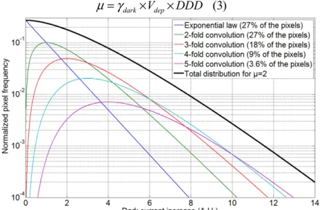
Figure 2 represents an example of a total dark current distribution (in logarithmic scale) for an exponential mean υdark = 1 Arbitrary Unit (A.U.) and for a mean number of interactions per
pixel µ=2. In that case, 13% of the pixels have not encountered a nuclear event and are not part of the dark current increase distribution. The total distribution is the sum of the exponential law (pixels with one interaction) and the n-fold convolutions (pixels with n interactions, n ≥ 2), all of them weighted by the Poisson’s coefficients (which represent the fraction of pixels that encountered n nuclear interactions with n ≥ 1). Because υdark is the mean
dark current per interaction, the mean dark current of the calculated total distribution is:
,
(4)
mean mod dark
DC
=
υ
×
µ
By combining Eq.(3) and Eq. (4) we obtain:
,
(5)
mean mod dark dark dep
DC
=
υ
×
γ
×
V
×
DDD
For nuclear interaction induced displacement damage, it has been shown that the mean dark current increase is proportional to the depleted volume and the DDD via the Universal Damage Factor (UDF) Kdark [37]:
, (6)
mean exp dark dep
DC =K ×V ×DDD
Since the model also needs to respect this condition on the calculated mean dark current increase, by combining Eq. (5) and Eq. (6) we obtain:
(7)
dark dark Kdark
υ
×γ
=Hence, γdark has to be inversely proportional to υdark and Eq. (3) becomes: , (8) mean exp dark dep dark dark DC K V DDD
μ
υ
υ
= × × =Fig. 2. Exponential dark current PDF, exponential n-fold convolutions and total dark current distribution for µ=2 with the empirical model (in logarithmic y-axis scale).
Consequently, the empirical model has only one degree of freedom which is the exponential mean υdark (because the mean dark current is given by the experimental distribution). Since
υdark represents the mean dark current increase per nuclear interaction, it can depend on the
neutron energy. Therefore, the best υdark is determined for each neutron energy using the least
square method between the calculated and the experimental distributions on all the pixel arrays irradiated at a given neutron energy. This approach allows to determine the dependence of υdark (exponential mean of the dark current distribution) on the particle energy. The three
first data points of the experimental distributions, which correspond to very low dark current increases, are not taken into account in the computation of the R-squared (R²) because they correspond, for the most part, to pixels which have not encountered nuclear events. Indeed, a small and homogeneous dark current increase of the entire pixel array is expected from the ionization due to silicon recoils within the silicon oxide. The very last data points (very high dark current increases) where the pixel count starts to become zero are also excluded from the calculation of R² because the statistics become too low. Once υdark has been determined for
each neutron energy, µ is determined for each irradiated pixel array using Eq.8 and the distributions are calculated using Eq. (2). They are compared to the experimental distributions to study the dependence of the dark current distribution on the pixel pitch, the pixel (photodiode) type and the DDD. The validity of this approach relies on the accuracy of the model, which is monitored for all the dark current distributions by the value of R².
3. Irradiated optical imagers and irradiation conditions
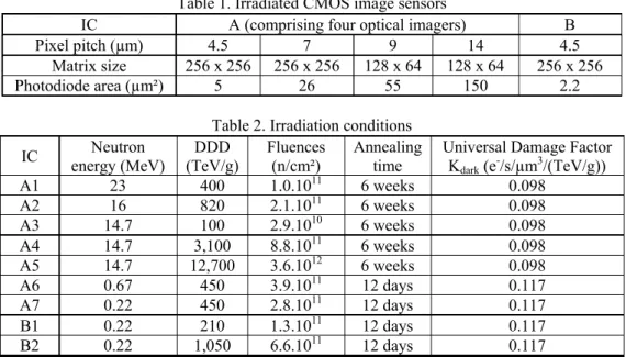
The main characteristics of the optical imagers irradiated in this work are presented in Table 1. Integrated Circuit (IC) A comprises four conventional photodiode 3T-pixel optical sensors (see Fig. 1(a) for a cross section of a 3T-pixel) with different pixel pitches, and IC B contains only one PPD 4T-pixel optical imager (see Fig. 1(b) for a cross section of a PPD pixel). Both ICs were fabricated using a commercially available 0.18 µm CIS process which is different than the one tested in [30]. It is important to note that, being on the same silicon die, the four optical sensors of a single IC A are irradiated with exactly the same conditions.
Table 1. Irradiated CMOS image sensors
IC A (comprising four optical imagers) B
Pixel pitch (µm) 4.5 7 9 14 4.5
Matrix size 256 x 256 256 x 256 128 x 64 128 x 64 256 x 256
Photodiode area (µm²) 5 26 55 150 2.2
Table 2. Irradiation conditions
IC energy (MeV) Neutron (TeV/g) DDD Fluences (n/cm²) Annealing time Universal Damage Factor K
dark (e-/s/µm3/(TeV/g)) A1 23 400 1.0.1011 6 weeks 0.098 A2 16 820 2.1.1011 6 weeks 0.098 A3 14.7 100 2.9.1010 6 weeks 0.098 A4 14.7 3,100 8.8.1011 6 weeks 0.098 A5 14.7 12,700 3.6.1012 6 weeks 0.098 A6 0.67 450 3.9.1011 12 days 0.117 A7 0.22 450 2.8.1011 12 days 0.117 B1 0.22 210 1.3.1011 12 days 0.117 B2 0.22 1,050 6.6.1011 12 days 0.117
Seven ICs A and two ICs B were irradiated with neutrons at various DDD and neutron energies; the irradiation parameters are detailed in Table 2. The DDD was calculated using tabulated NIEL values from [38]. The four optical sensors of IC A1 was irradiated with a non mono-energetic neutron beam centered on 23 MeV whereas all the other imagers were irradiated with monoenergetic neutron beams. Before the dark current measurement, the optical sensors were annealed at room temperature during 6 weeks for high energy neutron irradiated sensors (A1 to A5) and 12 days for low energy neutron irradiated sensors (A6 to B2). The UDF Kdark, which represents the mean dark current increase per unit dose and
volume, depends on the annealing time and measurement temperature [37]. It can be calculated using Fig. 3 in [37] for the annealing correction and using a dark current activation energy of 0.63 eV for the temperature correction (Eq. (11) in [37]). At T=22°C, Kdark is 0.098
e-/s/µm3/(TeV/g) for ICs A1 to A5 and 0.117 e-/s/µm3/(TeV/g) for ICs A6 to B2. 4. Experimental results
4.1. Estimation of the depleted volumes and depths
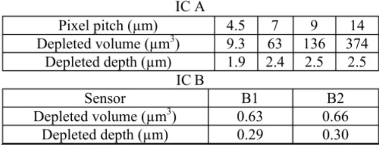
The depleted volume of the pixels can be estimated from Eq. (6) from the experimental DDD (Table 2), the experimental mean dark current increase and the UDF Kdark. Table 3 presents
the mean depleted volumes averaged on all the irradiated CIS. The depleted volumes spread from 0.7 µm3 for the small 4T-PPD pixel of sensor B to 370 µm3 for the largest 3T-pixel of
sensor A. Therefore, we can study the dependence of the dark current distribution (and test the empirical model) on a very wide range of depleted volumes.
The ratio between the mean depleted volume and the photodiode area (Table 1) also provides an estimation of the depleted depth (Table 3); it is about 2 µm for the conventional photodiodes and 0.3 µm for the PPD. The depleted depth of the conventional photodiodes slightly decreases with decreasing pixel pitch, which is expected due to three-dimensional effects on the depleted volume [39]. Indeed, in small pixel pitches, a larger part of the depleted volume lies into the highly P doped wells on the side of the photodiode [Fig. 1(a)], which reduces the ratio between the depleted volume and the photodiode area.
4.2. Effect of the pixel pitch (and depleted volume) on the dark current distribution
The dark current distribution dependence on the pixel pitch can be tested on ICs A, which contain four optical sensors with different pixel pitches (and very different depleted volumes, see Table 3) that can be irradiated in the same conditions. Figure 3 presents the experimental dark current distributions (data points) of the four optical imagers of IC A1 (irradiated with a neutron energy spectrum centered on 23 MeV and dose of 820 TeV/g) and of the optical sensors of IC A2 (irradiated with 400 TeV/g of 16 MeV neutrons) at T=22°C and after 6 weeks annealing. The dark current distributions are plotted in logarithmic scale on the y-axis
Table 3. Estimated depleted volumes and depleted depths IC A Pixel pitch (µm) 4.5 7 9 14 Depleted volume (µm3) 9.3 63 136 374 Depleted depth (µm) 1.9 2.4 2.5 2.5 ICB Sensor B1 B2 Depleted volume (µm3) 0.63 0.66 Depleted depth (µm) 0.29 0.30
(pixel count) to highlight the exponential shape of the dark current PDF. Because the 9 and 14 µm pixel pitch arrays contain eight times less pixels than the 4.5 and 7 µm pixel pitch arrays, their lowest pixel count is 8 instead of 1 as the distributions are normalized to have the same total pixel count for comparison. The distributions calculated with the model (with the optimum υdark) are represented by solid lines.
It is important to recall here that for a given IC, the sole free parameter is υdark, and that all
the other parameters required to plot the four distributions of a single IC are calculated (not adjusted) using the experimental mean dark current and the constant Kdark, as presented in the
previous section. Moreover, the exponential mean υdark must be the same for all the optical
sensors of a given IC because it represents the mean dark current increase per nuclear interaction (which should not depend on the pixel pitch but only on the neutron energy). The optimum exponential mean is υdark = 4.1.103 e-/s for both ICs here, and the goodness-of-fit are
respectively R² = 0.991 and R² = 0.980 for ICs A1 and A2. Therefore, it seems that the mean dark current increase per nuclear interaction is similar for 16 and 23 MeV neutrons.
Fig. 3. Experimental (points) and calculated (lines) distributions for sensors A1 (top figure, 23 MeV, 400 TeV/g) and sensor A2 (bottom figure, 16 MeV, 820 TeV/g) with υdark = 4.1.103 e-/s.
For a given IC, the agreement between the calculated and experimental distributions is good for all the pixel pitches with a same exponential mean υdark (which is supported by the
good R² values). Thus, the model is able to reproduce the dark current distribution for a wide range of pixel pitches (4.5 to 14 µm) and a very wide range of depleted volumes (9 to 370 µm3) with a same exponential mean υ
dark at a given particle energy. As shown later in Fig. 7,
the model also works in IC B (4T-PPD pixel) which has a very small depleted volume of 0.7 µm3. Therefore, the model can reproduce the dark current distribution dependence on the pixel
pitch without changing υdark, suggesting that the deformation of the dark current distribution is
when the pixel pitch changes is due to the superimposition of nuclear interactions in the pixels (hypothesis of the model). Indeed, the experimental dark current distribution is exponential in the smallest pixel pitch where most of the pixels have encountered a maximum of one nuclear interaction (µ << 1), and becomes distorted in larger pixel pitches where many pixels have suffered several nuclear events (µ ≥ 1), as predicted by the model.
4.3. Effect of the Displacement Damage Dose (DDD) on the dark current distribution
In order to analyze the evolution of the dark current distribution over a wide range of DDD, three identical ICs A (A3 to A5) were irradiated at the same neutron energy (14.7 MeV) but with very different DDD from 100 TeV/g to 12,700 TeV/g. Figure 4 presents the experimental (data points) distributions for these three ICs and the calculated distributions with the optimum exponential mean υdark (solid lines). The exponential mean, which represents the
mean dark current increase per nuclear interaction, must be the same for all the optical sensors of all the ICs because they were irradiated at the same neutron energy (υdark should depend
only on the particle energy, not on the DDD or pixel pitch). The optimum exponential mean here is υdark = 4.1.103 e-/s, as for ICs A1 (23 MeV neutrons) and A2 (16 MeV neutrons) in the
previous section. The goodness-of-fit is pretty good on all the sensors, with respectively R² = 0.955, R² = 0.986 and R² = 0.983 for sensors A3, A4 and A5.
At low DDD (IC A3), the distributions of all the pixel pitches (except the largest one) are exponential-like since most of the pixels have encountered one or no nuclear interaction (µ << 1). The dark current distribution of the 4.5 µm pixel pitch is not represented because very few pixels encountered nuclear events in this array; hence the statistics were too low to perform a
Fig. 4. (part 1): Experimental and calculated distributions for sensor A3 (14.7 MeV, 100 TeV/g), and with υdark = 4.1.103 e-/s.
proper analysis of the results. Overall, the statistics are low for this IC because of the very low DDD, which explains the higher variability of the data points and the slightly lower goodness-of-fit (R² = 0.955). On the other hand, at high DDD (sensor A5), all the dark current distributions (except in the smallest pixel pitch) are Gaussian shaped because the mean number of nuclear interactions per pixel is very high. Even the smallest pixel pitch distribution starts to be distorted because µ is slightly higher than 1.
In conclusion, the DDD has the same effect than the depleted volume on the dark current distribution, leading to a deformation of the exponential distribution when the mean number of nuclear interactions per pixel exceeds one. The agreement between the model and the data is good for all the DDD with a same exponential mean υdark, which shows that the modelcan
reproduce the dark current distribution dependence on the DDD with a same υdark for a given
particle energy. Therefore, the model can predict the dark current distributions for very different DDD (two orders of magnitude) in very different depleted volumes (9 to 370 µm3 as
shown in the previous section) without changing any parameters for a given particle energy.
Fig. 4. (part 2): Experimental and calculated distributions for sensors A4 (top figure, 14.7 MeV, 3,100 TeV/g) and A5 (bottom figure, 14.7 MeV, 12,700 TeV/g) with υdark = 4.1.103 e-/s.
4.4. Effect of the neutron energy on the dark current distribution
In the two previous sections, it was observed that the optimum exponential mean was υdark =
4.1.103 e-/s (for 6 weeks annealing) for 14.7, 16 and 23 MeV neutrons. Therefore, it seems
that the exponential mean (mean dark current increase per nuclear interaction) is very similar for all these neutron energies. Figure 5 and Fig. 6 present the dark current distributions of ICs A7 and A8 irradiated at lower neutron energies (respectively 0.67 MeV and 0.22 MeV) and measured at T=22°C after 12 days of annealing.
Since the annealing time is shorter than for high-energy neutron irradiated sensors, the UDF Kdark is higher (0.117 e-/s/µm3/(TeV/g) instead of 0.098 e-/s/µm3/(TeV/g)). The exponential
mean, which represents the mean dark current increase per nuclear interaction, must have the same dependence on annealing (and on measurement temperature) than the UDF (which
Fig. 5. Experimental (points) and calculated (lines) distributions for sensor A6 (0.67 MeV, 450 TeV/g) with υdark = 4.9.103 e-/s (dashed lines) and υdark = 2.4.103 e-/s (solid lines).
Fig. 6. Experimental (points) and calculated (lines) distributions for sensor A7 (0.22 MeV, 450 TeV/g) with υdark = 4.9.103 e-/s (dashed lines) and υdark = 1.4.103 e-/s (solid lines).
represents the mean dark current increase per unit volume and dose). Hence, the exponential mean of the high-energy neutron irradiated optical sensors (υdark = 4.1.103 e-/s for 6 weeks
annealing) should be equal to υdark = 4.9.103 e-/s after 12 days annealing [37]. As can be seen
in Fig. 5 and Fig. 6, the calculated distributions with υdark = 4.9.103 e-/s (dashed lines) poorly
reproduce the experimental distributions and the R² is very low (respectively R² = 0.792 and R² = 0.597). The exponential mean is overestimated because the experimental distributions are steeper than the calculated distributions. The optimum exponential mean for ICs A6 and A7 are respectively υdark = 2.4.103 e-/s and υdark = 1.4.103 e-/s; the corresponding calculated
distributions are plotted in solid lines. In that case, the R-squared retrieve good values of respectively 0.990 and 0.983. Therefore, the exponential mean seems to decrease at low neutron energies (0.22 and 0.67 MeV) compared to high energy neutrons (14.7 to 23 MeV), suggesting that the mean dark current increase per nuclear interaction is lower. We should note that, in the small pixel pitch optical imagers of IC A6 (0.67 MeV neutrons), the data points corresponding to the highest dark current increases have a higher pixel count than the model, which is an effect that was not observed for high energy neutrons. It is even more pronounced in the small pixel pitches of sensor A7 (0.22 MeV neutrons). Therefore, it seems that the dark current PDF of a nuclear interaction slightly diverges from an exponential law for low energy neutrons.
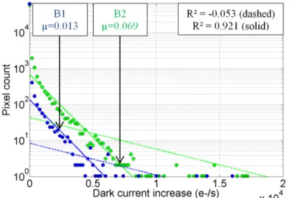
Eventually, Fig. 7 presents the dark current distributions for the two 4T-PPD optical sensors B1 and B2, irradiated at 0.22 MeV. The optimum exponential mean is υdark = 1.2.103
e-/s, which is similar to the optimum exponential mean of the 3T optical imagers irradiated at
the same neutron energy (IC A8, υdark = 1.4.103 e-/s). This shows that the exponential mean is
independent on the photodiode type (conventional or PPD). The slight difference may be due to the poor statistics in ICs B1 and B2 (R² = 0.921), because very few pixels have encountered nuclear events (the mean number of interactions per pixel µ is very low, respectively 0.011 and 0.058 for ICs B1 and B2). Once again, the dark current PDF on the nuclear interaction seems to deviate from an exponential law at this low energy, which can be seen by the numerous data points located above the model at large dark current increases.
Fig. 7. Experimental (points) and calculated (lines) distributions for sensors B1 (0.22 MeV, 210 TeV/g) and B2 (0.22 MeV, 1,050 TeV/g) with υdark = 4.9.103 e-/s (dashed lines) and υdark = 1.2.103 e-/s (solid
5. Discussion
5.1. Effect of the particle energy on the exponential mean of the dark current distribution In the previous work on this model [30], an average exponential mean of υdark = 6.2.103 e-/s
was obtained for both high-energy neutrons (14.7 to 23 MeV) and very high-energy protons (60 to 500 MeV). The dark current was measured at T=23°C and after three weeks annealing, hence the UDF was slightly higher than for the high-energy neutron irradiated CIS tested in this work (0.118 e-/s/µm3/(TeV/g) instead of 0.098 e-/s/µm3/(TeV/g)). Hence, the exponential
mean for high-energy neutrons in this work (υdark = 4.1.103 e-/s at T=22°C and for 6 weeks
annealing) should be equal to υdark = 4.9.103 e-/s in the previous work conditions [37] because
υdark isproportional to Kdark. This is lower than the average exponential mean in the previous
work, which suggests that high-energy neutrons lead to a lower exponential mean than very high energy protons. Moreover, the experimental results in this work have shown that the exponential mean decreases at lower neutron energies. Therefore, the exponential mean (which represents the mean dark current increase per nuclear interaction) seems to decrease for decreasing particle energies, which could be due to a decrease of the mean damage energy per nuclear interaction. Indeed, the mean dark current increase per nuclear interaction should be proportional to the mean damage energy per interaction because the UDF should apply. 5.2. Theoretical and experimental estimation of the mean damage energy per interaction
The theoretical mean damage energy per nuclear interaction can be calculated from the PDF of the nuclear scattering energy. In this calculation, only elastic nuclear interaction in silicon will be considered and inelastic nuclear reactions will be neglected for simplicity. Figure 8 presents the PDF of the cosine of the elastic scattering angle (i.e. the angle between the incident and reflected neutron trajectories) for various neutron energies, from [40]. The energies were chosen as close as possible to the experimental energies tested in this work for comparison.
These PDF correspond directly to the nuclear elastic scattering energy PDF (i.e. the energy transmitted to the PKA, noted EPKA) because the scattering energy is proportional to the
cosine of the scattering angle [41]:
Fig. 8. PDF of the cosine of the elastic scattering angle in the Center of Mass (C.M.) axis system for various neutron energies in logarithmic scale, from [40]. This corresponds directly to the PDF of the PKA energy (zero for cos (θ) = 1, Emax for cos (θ) = -1).
( )
( )
(1 cos ) (1 cos ) 4 (10) ( 1)² 2 2 PKA n max Z E E E Zθ
θ
− − = = +Where Z is the atomic mass of the target atom, En is the neutron energy and Emax is the
maximum elastic scattering energy (for cos (θ) = -1):
4 0.133 for Si (11) ( 1)² max n n Z E E E Z = = +
Elastic scattering cosine angle PDF can also be found in [41] for comparison, for several energies between 600 keV and 14.6 MeV. From Fig. 8, the mean PKA energy can be calculated for each neutron energy. The results are given in Table 4 and show that the mean PKA energy decreases with decreasing neutron energy.
The damage energy PDF can be deduced from the elastic scattering energy PDF by applying the Lindhard partition function [42], which represents the fraction of the PKA energy converted into displacement damage (the rest being deposited into ionization). The damage energy PDF are presented in Fig. 9 and the corresponding mean damage energies are reported in Table 4.
These values are in agreement with litterature; for example, the elastic mean damage energy at 20 MeV is 85 keV in [31]. On one hand, the mean damage energy per elastic nuclear interaction is almost equal for 14.1 and 20 MeV neutrons, which could explain why a similar exponential mean is obtained in the experimental results for 14.7, 16 and 23 MeV neutrons. On the other hand, the mean damage energy is much lower at low neutron energies (200 and 605 keV), which could explain the lower exponential mean for 0.22 and 0.67 MeV
Fig. 9. Damage energy PDF calculated from the PKA energy PDF of Fig. 8 using the Lindhard partition function [42].
Table 4. Mean PKA and displacement damage energies Neutron energy
(MeV) energy (keV) Mean PKA Theoretical elastic mean damage energy (keV)
0.200 13.1 10.7
0.605 28.3 21.0
5.8 184 72.0
14.1 241 75.3
neutrons in the experimental results.
The mean damage energy per nuclear interaction can also be estimated from our experimental results. Indeed, υdark is the mean dark current increase per nuclear interaction and
Kdark is the mean dark current increase per unit dose and volume. Then, from Eq. (6), ρ/υdark
must correspond to the mean damage energy per nuclear interaction (where ρ, the density of silicon, appears because the dose in Kdark is expressed per unit mass). The values of υdark, γdark
= Kdark / υdark and the mean damage energy ρ/υdark are presented in Table V for all the
experimental neutron energies.
The experimental mean damage energy decreases with decreasing neutron energies like the theoretical mean damage energy. The theoretical (Table 4) and experimental (Table 5) mean damage energies are quite close for high-energy neutrons (respectively 76 and 97 keV). The higher value for the experimental mean damage energy could be due to the contribution of inelastic nuclear reactions, which are not taken into account in the computation of the theoretical mean damage energy. Indeed, in [31], the mean damage energy considering both elastic and inelastic interactions is 115 keV for 14 MeV neutrons (which is close to our experimental result of 97 keV), whereas it is only 85 keV with elastic interactions alone. In [32], the mean damage energy for nuclear interactions is 85 keV for 20 MeV protons (which is close to 14.7 MeV neutrons) but it is about 120 and 165 keV for 60 and 500 MeV protons respectively. These higher mean damage energies for very high energy protons could explain why a higher average exponential mean was found in the previous work [30] compared to high-energy neutrons alone here. Eventually, for low energy neutrons (200 and 600 keV), the experimental damage energy is about twice as high as the theoretical mean damage energy, which suggests that the UDF Kdark could be higher at these energies. Because low energy
neutrons produce low energy PKA, it is possible that there are often no sub-cascades, which could lead to a more sparse damage and to a lower recombination of the Frenkel pairs [23]. Consequently, the amount of stable defects (and thus of dark current increase) per unit damage could be higher.
Overall, the similar trend observed for theoretical and experimental mean damage energies per nuclear interaction with respect to neutron energy (and the close values obtained for high-energy neutrons) confirms that the exponential PDF observed at low doses and in small depleted volumes corresponds to the dark current PDF of nuclear interactions rather than single defects (as supposed in section 2), and that the convolution behavior of the dark current distribution at higher doses or in larger volumes corresponds to the superposition of nuclear interactions in the pixels.
5.3. Absence of border effects on the dark current distribution
From Eq. (11), it can be seen that high-energy neutrons (23 MeV) produce elastic recoils with energies up to 3 MeV. A 3 MeV PKA has a range of 2.3 µm in silicon [43], which is comparable to the dimensions of the smallest depleted volume in IC A (about 3.5 x 1.5 x 2 µm for the 4.5 µm pitch pixel) and to the smallest distance between the depleted volumes of adjacent pixels (about 1 µm). Hence, a damage cascade could start in the depleted volume and end outside of it, or inversely. It could also start in the depleted volume of one pixel and finish
Table 5. Experimental damage energies Neutron
energy (MeV) υdark (e
-/s) at T=22°C and
for 12 days annealing γdark(g/TeV/ µm = Kdark / υ3dark) energy ρ/γExp. mean damage dark (keV)
0.22 1.2-1.4.103 8.4-9.8.10-5 24-28
0.67 2.4.103 4.9.10-5 48
in the depleted volume of an adjacent pixel. These border effects should lead to a reduction of the mean dark current increase per nuclear interaction, because the damage located outside of the depleted volume would not contribute to the dark current increase. The border effects should have a significant impact on the dark current distribution of small pixel pitch optical sensors [32, 35]; in particular they should reduce the exponential mean for small pixel pitches compared to large pixel pitches. However, it has been seen in the experimental results that the dark current distributions of all the pixel pitches of a same IC A were accurately reproduced by the model with a same υdark; hence the border effects seem negligible. This is not surprising
since high-energy elastic PKA are very rare for high-energy neutrons [Fig. 8]. The PPD of sensor B has dimensions of about 2 x 1 x 0.3 µm (Table 3), and was irradiated with 0.22 MeV neutrons which produce elastic PKA of 23 keV or lower. In that case, the PKA range is limited to about 35 nm [43], which is much smaller than the PPD depleted volume dimensions; hence the border effects are also negligible in this sensor.
6. Conclusion
Many space missions and nuclear experiments require optical imagers with outstanding low-light performances to be used in radiation environments. In irradiated CIS or CCD, the main factor limiting low light performance is the dark current increase. It needs to be predicted for various optical sensors and radiation environments in order to properly mitigate the image quality degradation. In this work, the effect of several optical imager features and radiation conditions on the dark current increase distribution has been studied independently: the pixel pitch (and consequently the depleted volume), the pixel/photodiode type, the particle fluence (DDD) and the particle energy. The effect of each parameter has been studied with the help of an empirical model, which assumes an exponential law as the dark current PDF of one nuclear interaction and convolves it when nuclear interactions superimpose in the pixels. It was observed that this model accurately calculates the dark current distributions of all the optical sensors irradiated at a same particle energy without changing any model parameter, regardless of the pixel pitch, photodiode type and DDD. The depleted volume and DDD were observed to have a similar and independent effect on the dark current distribution, producing a progressive deformation of the exponential law towards a Gaussian law when the mean number of nuclear interactions per pixel exceeds 1. Neither the pixel/photodiode type nor the technology (which is different than in [29]) seems to have an effect on the dark current distribution. Eventually, it has been shown that the model works without changing any parameter for high energy neutrons (14.7 to 23 MeV) but requires an adjustment of the exponential mean (which represent the mean dark current increase per nuclear interaction) at lower neutron energies. This effect has been attributed to the lower mean damage energy per nuclear interaction for low energy neutrons.
In conclusion, the empirical model is based on hypotheses which seem to be representative of the real properties of the dark current distribution, and it can be used to predict the dark current increase distribution for various silicon solid state optical image sensors and radiation environments. For the neutron energies tested in this work (for which υdark has been
determined), the dark current increase distribution can be predicted in a given optical detector (for which the depleted volume is known) and for a given radiative environment (particle energy and fluence) using the corresponding exponential mean υdark and using Eq. (3) to
determine µ from the depleted volume, the DDD, υdark and Kdark from [36] (with γdark = Kdark /
υdark from Eq. (7)). For other neutron energies or other particles (protons but maybe also
heavier ions), the model can be used as soon as the exponential mean has been determined. It allows taking the dark current increase into account when designing an optical imager instrument, in order to choose an appropriate mitigation technique and to limit the dark current degradation.


![Fig. 8. PDF of the cosine of the elastic scattering angle in the Center of Mass (C.M.) axis system for various neutron energies in logarithmic scale, from [40]](https://thumb-eu.123doks.com/thumbv2/123doknet/3158129.89998/15.918.260.661.610.876/cosine-elastic-scattering-center-various-neutron-energies-logarithmic.webp)
![Fig. 9. Damage energy PDF calculated from the PKA energy PDF of Fig. 8 using the Lindhard partition function [42]](https://thumb-eu.123doks.com/thumbv2/123doknet/3158129.89998/16.918.282.667.423.688/damage-energy-calculated-energy-using-lindhard-partition-function.webp)

