This is an author-deposited version published in:
http://oatao.univ-toulouse.fr/
Eprints ID: 7955
To link to this article: DOI: 10.1109/TNS.2012.2203317
URL:
http://dx.doi.org/10.1109/TNS.2012.2203317
To cite this version:
Virmontois, Cédric and Goiffon, Vincent and Magnan,
Pierre and Girard, Sylvain and Saint-Pé, Olivier and Petit, Sophie and Rolland,
Guy and Bardoux, Alain Similarities Between Proton and Neutron Induced
Dark Current Distribution in CMOS Image Sensors. (2012) IEEE Transactions
on Nuclear Science, vol. 59 (n° 4). pp. 927-936. ISSN 0018-9499
O
pen
A
rchive
T
oulouse
A
rchive
O
uverte (
OATAO
)
OATAO is an open access repository that collects the work of Toulouse researchers and
makes it freely available over the web where possible.
Any correspondence concerning this service should be sent to the repository
administrator:
[email protected]
Similarities Between Proton and Neutron Induced
Dark Current Distribution in CMOS Image Sensors
Cedric Virmontois, Student Member, IEEE, Vincent Goiffon, Member, IEEE, Pierre Magnan, Member, IEEE,
Sylvain Girard, Senior Member, IEEE, Olivier Saint-Pé, Sophie Petit, Guy Rolland, and Alain Bardoux
Abstract—Several CMOS image sensors were exposed to
neu-tron or proton beams (displacement damage dose range from 4 TeV/g to 1825 TeV/g) and their radiation-induced dark current dis-tributions are compared. It appears that for a given displacement damage dose, the hot pixel tail distributions are very similar, if nor-malized properly. This behavior is observed on all the tested CIS designs (4 designs, 2 technologies) and all the tested particles (pro-tons from 50 MeV to 500 MeV and neutrons from 14 MeV to 22 MeV). Thanks to this result, all the dark current distribution pre-sented in this paper can be fitted by a simple model with a unique set of two factors (not varying from one experimental condition to another). The proposed normalization method of the dark current histogram can be used to compare any dark current distribution to the distributions observed in this work. This paper suggests that this model could be applied to other devices and/or irradiation con-ditions.
Index Terms—Active pixel sensor (APS), CMOS image sensor
(CIS), dark current distribution model, displacement damage dose (DDD), monolithic active pixel sensor (MAPS).
I. INTRODUCTION
C
MOS image sensors (CIS) have to be able to operate in intense radiation environments for their use in many sci-entific applications, such as space instruments. For an irradiated CIS, also called an Active Pixel Sensor (APS), a key issue re-mains the dark current increase with the radiation dose [1]–[23]. Ionization and displacement damage effects contribute to this degradation of the CIS performance. Many studies focus on the ionizing effect which leads to a uniform increase of the dark current in pixel arrays [13]–[23]. On the contrary, fewer studies have been dedicated to displacement damage in CIS [1], [12], and, most of the time, previous workers present proton irra-diation results which cumulate total ionizing dose (TID) anddisplacement damage dose (DDD). The hot pixel tail of the dark current distribution that appears after proton irradiations is commonly attributed to the displacement damage effect on CIS. However, the mechanisms involved in this non-ionizing effect are not completely understood and dedicated studies are required. Moreover, using the last generation of CIS [7] and the hardened sensors against TID [2], [5], ionizing radiation effects are clearly reduced and displacement damage becomes the main issue for CIS dedicated to space and scientific applications in-volving radiation environment.
Previous studies on CIS [12], emphasized the scaling be-tween the mean dark current increase and DDD using the Universal Damage Factor (UDF) introduced by Srour [24]. This universality implies that independently of the particle type and energy, the final mean dark current increase remains proportional to DDD using the factor, if electric field enhancement effects are negligible. In addition to the av-erage increase, several studies in CIS show large dark signal non-uniformity (DSNU) after irradiation conditions leading to displacement damage [1]–[12]. All the observed dark current distributions have a common hot pixel tail which behaves as a quasi-exponential decrease. These hot pixel tails were attributed to inelastic nuclear interactions in [1], elastic and inelastic nu-clear interactions in [12] whereas electric field enhancement (EFE) was also proposed in [2], [3]. In these previous studies, EFE theory [25] correctly predicts the dark current distribution for CIS processed using technology nodes until gen-eration and not dedicated to imaging. For these devices, a high electric field was evidenced in the photodiode depletion region. But, thanks to the recent development of CIS process and the will of CIS manufacturers to decrease the dark current level (and thus to reduce the highest electric fields), EFE appears less frequent in sensors manufactured using CMOS processes dedicated to CIS (the so called CIS processes). Therefore, EFE does not seem to contribute significantly to DSNU [12].
The goal of this paper is to compare the displacement damage-induced dark current increase caused by protons and neutrons in CMOS image sensors manufactured using a CIS process. The devices under investigation consist of pixels using conventional photodiodes and using pinned photodiodes [26], [27].
The first part focuses on the experimental data. The mean dark current increase, the dark current distribution changes and the activation energy of the dark current are investigated after proton and neutron irradiations. This set of results comes from a significant number of CIS with different process and design. Protons have been selected for this study since most of the
pub-lished material on displacement damage effects in silicon im-agers uses this particle (mainly because protons are one of the main particles of interest for space applications). As regards neutrons, the main advantage of their use [10]–[12] is to re-duce the total ionizing dose and is supposed to reveal solely displacement damage effects. This section shows an interesting similarity between proton and neutron irradiations at equivalent DDD: the dark current increase exhibits the same exponential behavior.
The second part presents the previous models used to pre-dict the dark current (increase) distributions. The first one is a physical model developed using charge injection devices (CID) [30]–[33] and was improved and adapted for charge-coupled devices (CCD) [34], [35]. It is based on the deposit energy in the pixel microvolume (calculated with Monte-Carlo simula-tion) and the number of interactions per pixel (estimated using particle interaction cross section). To the best of our knowledge, few studies are based on this physical model and adjusted to pre-dict dark current increase distribution in CMOS image sensors [2], [3], [12]. Other models developed to predict dark current in-crease distribution in CMOS image sensors are based on fitting methods [9], [10] applied to only one device (in each paper).
The third part is dedicated to the presentation of a normaliza-tion method and an engineering model aimed at describing the whole set of available data and based on the similarity reported in the first part. This model is based on the empirical analysis of the large number of tested CIS in this study. The common exponential distributions obtained after irradiation tests are ex-plored and a set of two factors ( and ) appear to be sufficient to forecast the hot pixel tail distributions of the tested CIS. The method developed in this paper is more direct than the physically based model and shows a direct link between the dark current increase distribution and the displacement damage dose. It could become a useful tool to compare the dark current increase distributions of silicon imagers to the data presented here and it could also possibly have an impact on the design of CIS dedicated to radiation environment.
Finally, a conclusion is drawn concerning the possible ben-efit of using such an engineering model and the possible conse-quence of this similarity between dark current distributions at a given DDD.
II. EXPERIMENTALDETAILS
The studied CMOS image sensors were manufactured with several CIS processes, several pixel pitches, and several tech-nologies. These circuits were manufactured in a com-mercial CIS process. Table I lists the 18 studied devices. De-vices IC are -pitch 128 128 pixel arrays with 3T-pixels using conventional photodiodes and are processed in a silicon epitaxial layer. Devices DO and PI are respectively 7 and -pitch 128 128 pixel arrays with 3T-pixels using conventional photodiodes and are processed in silicon bulk. De-vices UL are -pitch 256 256 pixel arrays with 4T-pixels using pinned photodiodes [26], [27] and are processed in silicon epitaxial layer.
Sensors were exposed to neutron beams at Université Catholique de Louvain (UCL) facility and CEA DAM Valduc. Proton irradiations were performed at TRIUMF (Vancouver),
TABLE I
IRRADIATIONCHARACTERISTICS.
at Kernfysisch Versneller Instituut (KVI) and at UCL. The total DDD ranged from 4 to 1825 TeV/g. Irradiations were performed at room temperature and devices were grounded during tests. Table I provides all irradiation characteristics.
Dark current measurements were carried out three weeks after irradiation, inside an air oven at . Other tests with temperatures ranging from to were also performed to calculate the activation energy of the dark current.
III. DARKCURRENTINCREASE
A. Mean Dark Current Increase
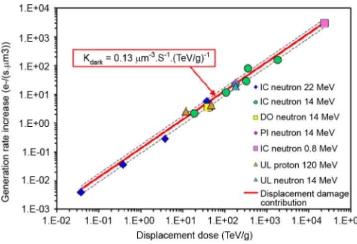
The large number of pixels in the CIS arrays allows the ob-taining of a statistical distribution of the dark current increase. First, the average value of the distribution is investigated. As we know the depleted volume of the in-pixel photodiode using TCAD physical simulations, we can deduce the mean genera-tion rate increase per pixel. Therefore, this value can be com-pared to those obtained using other devices, such as isolated transistor junctions or large photodiodes with depleted volume one thousand times larger than that of the in-pixel photodiode. Thus, we can compare our experimental results to the one used to determine the UDF [24]. Fig. 1 presents the mean genera-tion rate increase for the studied devices following the DDD. Most of the results come from 3T-pixels irradiated with neu-trons. It is important to remember that neutron irradiations bring mainly DDD. Therefore, these particles are useful tools to solely study displacement damage in CIS [12]. In addition, results from 4T-pixels using pinned photodiodes irradiated with neu-trons and protons are reported. The generation rate increase con-tribution due to displacement damage is estimated using the UDF [24] and also plotted in the figure. The UDF value was extrapolated at the temperature of our measurements and for
Fig. 1. Mean dark current increase measured on the studied pixel arrays. Es-timation of dark current due to displacement damages is calculated using the universal damage factor [24]. Independently of the particle energy and the flu-ence, the results agree with estimated displacement contribution.
the three week annealing at ambient temperature. The experi-mental results agree with the displacement damage contribution estimated using the UDF, for the whole range of energy and fluence explored. It emphasizes the relevance of this factor in CIS and confirms that the dark current increase due to displace-ment damage comes from electro-active defects located inside the space charge region of the in-pixel photodiode.
We do not represent proton results for 3T-pixel CIS because their average dark current value is influenced by TID. Indeed, ionization effect induces another source of dark current in CIS [13]–[23] which is mainly due to interface states located at the contact between the photodiode space charge region and the iso-lation oxide [36]. Therefore the mean generation rate of such ir-radiated devices is one order of magnitude above neutron results at the same DDD [12] and hides displacement damage effects, at least on the average value. On the contrary, the results for the proton-irradiated 4T-pixel devices are plotted in the figure. Such devices consist of a buried photodiode with a depleted region well-protected from the surrounding oxides by heavily doped P layers. Therefore, a 4T-pixel using a pinned photodiode is natu-rally more tolerant against TID and the results depicted in Fig. 1 demonstrate that displacement damage is mainly responsible for the dark current increase in such devices.
It is particularly important to note that negative bias voltage on the transfer gate of the 4T-pixel using a pinned photodiode [37] is used to reach these performances for all results presented in this study. If this bias is not correctly applied, the transfer gate acts as a dark current source and it is sensitive to TID.
B. Dark Current Distributions
This part is dedicated to the dark current distribution ob-served after irradiations. The large number of pixels from each CIS array provides an interesting statistic for the displacement damage-induced dark charge generation rate. Therefore, we in-vestigated the distribution of the pixel dark current after proton and neutron irradiations.
Fig. 2 presents dark current distributions obtained after proton tests. Energies used range from 50 to 500 MeV and the DDD
Fig. 2. Dark current distributions obtained after proton irradiations at several Displacement Damage Doses. A common exponential behavior is observed on the hot pixel tail and the Gaussian part of the distribution is switched to higher dark current. This switch is mainly due to the total ionizing dose.
Fig. 3. Dark current distributions after neutron irradiations at several displace-ment damage doses. As a large amount of pixels stay in the initial Gaussian, we deduce that few pixels are impacted in this dose range. However for the highest dose, all pixels seem to be impacted and the distribution shape is changed.
and TID associated range respectively from 19 to 259 TeV/g and from 8 to 93 . The initial distribution is added in a green dash line. We observe two distinct parts for each distri-bution. The first trend, the Gaussian, consists of the main pixel population and the second trend, the hot pixel tail, consists of a smaller number of pixels. In the proton irradiation case, both parts increase with radiation dose. The mean of the Gaussian part switches to higher dark current and the standard deviation increases too. Concerning the hot pixel tail, it also shifted to higher current value but kept its exponential behavior.
Fig. 3 illustrates the results obtained after neutron irradia-tions. In this case, the DDD range from 4 to 1825 TeV/g (the corresponding TID is neglected here). As for protons, we ob-serve two trends, the Gaussian and the pixel tail. In contrast to protons, the Gaussian part stays at the initial value, except for the higher dose. This effect implies most of the pixels are not impacted and keep their initial dark current value. At the highest dose, the Gaussian is distorted and all the population is impacted. Similarly to the proton results, the hot pixel tail shifts with increasing radiation dose which is mainly displace-ment damage in the case of neutrons. We also observe the ex-ponential tail behavior. To investigate this tail, the dark current
Fig. 4. Dark current increase distributions after neutron irradiations at several Displacement Damage Doses. Exponential behavior is observed for all distri-butions. For the highest dose, this behavior changes and all pixel seem to be impacted by displacement damage.
increase distribution is plotted in Fig. 4. Using this representa-tion (semi-logarithmic scale), we observe the clear exponential behavior. The exponential behavior keeps the same slope, that is to say, in terms of probability distribution, the same average value of the exponential distribution. The number of pixels in-creases in the distribution following the dose and the exponen-tial behavior appears to be shifted to higher dark current values with the radiation dose. This phenomenon differs slightly when most of the pixels exhibit a dark current increase due to the ir-radiation. At this point, the dose is around 300 TeV/g for IC devices. For higher doses the exponential behavior is distorted and we assume that particular pixels are impacted by more than one displacement damage interaction.
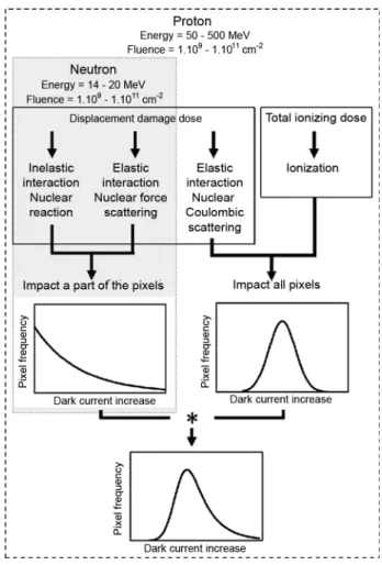
In order to understand the physical degradation of the distributions, it is important to identify the interactions in-volved during particle irradiations. Fig. 5 describes the main interactions involved during proton and neutron irradiation for the investigated ranges of energy and fluence. Neutrons deposit mainly displacement damage dose and the interactions involved are nuclear reaction (inelastic interaction) and interac-tion through nuclear force scattering (elastic interacinterac-tion). These interactions create bulk defects in silicon. The cross sections of these interactions are pretty small (compared to Coulombic scattering of protons in silicon), leading to an average number of interactions per pixel microvolume around or below one, for displacement damage dose under 300 TeV/g [12]. Thus, a neutron creates electro-active bulk defects in few pixels. The induced defects generate dark charges in few pixels leading to the hot pixel tail observed in Fig. 4 where experimental data are plotted.
Protons deposit total ionizing dose and displacement damage dose. Due to their charges, the protons induce an ionizing effect. This effect leads to the build up of interface states in CIS oxides and increases the overall dark current. The frequency of the process is important and, even for low TID, all pixels are impacted. Therefore, the dark current distribution due to proton TID corresponds to a Gaussian (or Gamma) [13]–[23]. Regarding proton-induced displacement damage, the charge of the particle brings one more different type of interaction
Fig. 5. Description of the damage induced by proton and neutron irradiations.
compared to a neutron. This interaction is the elastic nuclear Coulombic scattering. For the tested range, the interaction cross section of this effect is important. Therefore, even at low DDD, this elastic interaction induced bulk defects in all CIS pixels leading to a Gaussian (or Gamma) dark current increase distribution. Previous studies [30]–[35] assumed that all dis-placement damage interactions are independent and the final dark current distribution corresponds to the convolution of the dark current increase provided by each interaction (limitation of this affirmation exists when EFE is present or depending on the sensitive volume size). However, as regards our exper-imental results, we cannot confirm such a hypothesis because the distribution obtained after proton irradiations does not seem to correspond well to the pure convolutions of Gaussian or Gamma distributions.
C. Origins of Dark Current
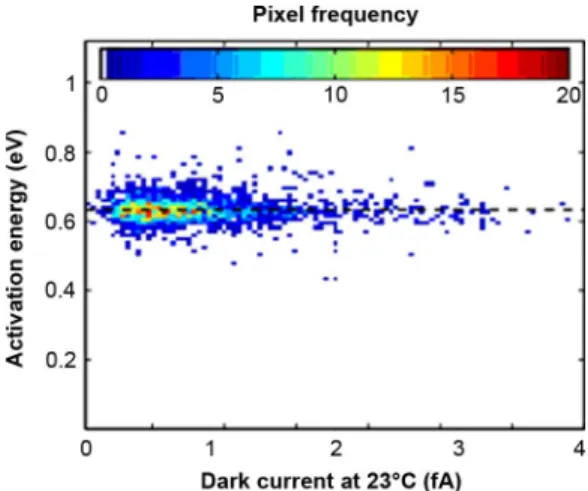
Proton and neutron irradiations induce displacement damage. These effects induce electro-active defects which affect the sensor dark current. In order to investigate the origins of the dark current and confirm that it comes from the generation center in the depleted volume of the photodiode, we calculate the activation energy of the dark current. All CMOS image sensors are investigated. Fig. 6 presents the dark current activa-tion energy distribuactiva-tion for device IC 2 irradiated with 22 MeV
Fig. 6. Device IC 2 irradiated with 22 MeV neutrons presents activation energy centered on the silicon mid-gap value (0.6 eV) for all pixels even those with the higher dark current. Classic SRH generation mechanism occurs in each pixel after irradiation.
neutrons. Equation (1) is used to calculate activation energy (Ea)
(1) where is the dark current, k is the Boltzmann constant and T is the temperature.
The activation energy value is found to be around 0.6 eV for almost all the pixels of all the tested CIS, even for the pixels with the highest dark current values (hot pixels). These results confirm that the dark current originates from a classic Shockley-Read-Hall (SRH) generation mechanism induced by defects lo-cated in the depleted volume of the in-pixel photodiode. These results also emphasized the energy level of the defects around the silicon mid-gap value and no enhancement factor appears to be involved (e.g., EFE [2], [3], [25]). It should be emphasized that such effect enhances the dark current and reduces its acti-vation energy. This conclusion is important because EFE was observed in CIS manufactured using processes not dedicated to imaging and was taken into account in previous models of the dark current increase due to displacement damage. It does not appear necessary for the devices studied here. This discrepancy is attributed to the recent development of CIS manufacturing process that aimed at reducing the dark current level as much as possible, especially by limiting high electric field regions in the photodiode.
IV. EXISTINGMODEL OF THEDARKCURRENTINCREASE
DISTRIBUTIONS
Several approaches are investigated to understand and to model the dark current distributions due to displacement damage in solid state imagers [2], [3], [9], [10], [12], [30]–[35]. Previous studies of CIS [2], [3], [12] are based on the physical model developed in [30]–[33]. This approach is aimed at esti-mating the dark current increase distributions. The prediction is firstly based on the construction of the damage energy distri-bution induced by a particle interaction in silicon microvolume (this volume is defined as the photosensitive depleted volume in
the pixel). Such construction requires performance of a Monte Carlo simulation or use of the GEANT4 calculation code for each considered particle type or energy. These authors [30]–[33] provide results of their simulations for protons. In [33], tables are provided for proton energy ranging from 1 MeV to 1000 MeV. Using such results we can obtain the energy distribution for each interaction. Then, using elastic and inelastic interaction cross section, the average number of interactions per depleted microvolume can be estimated. As previously mentioned (see Section III-B), the inelastic cross section is weak for the en-ergy and fluence ranges investigated. This implies an average inelastic interaction per microvolume around 1. Therefore, a Poisson statistic is introduced to correctly weight and model the inelastic distribution [30]–[33] (for neutron irradiations, elastic interaction cross section is as weak as an inelastic one [12] for studied DDD ranges. Thus the Poisson statistic is introduced in both interaction cases to build the distributions). As authors as-sume that interactions are independent from one type to another, the final energy distribution per interaction in the microvolume corresponds to the convolution of the elastic and inelastic dis-tributions. Finally, the energy distribution is compared with the experimental dark current increase distribution to obtain a con-version factor between damage energy and current. This first physical model correctly predicts dark current increase in CID for energy around 12 and 22 MeV and the conversion factor was found around . However, the model is less relevant for higher energy near 63 MeV.
After, the same approach is used in CCDs [34]. In order to im-prove the model, the Gamma distribution is used instead of the Gaussian to build the energy distribution. The author obtained a correct prediction for 10 and 60 MeV proton irradiations. The conversion factor between deposited energy and current was found to be related to the UDF [24]. In [35], commercial CCDs are investigated and the authors use the depleted volume as a fitting parameter.
Particular attention must be paid to the size of the micro-volume using this model. If the considered micro-volume becomes as small as the maximum interaction cascade, the energy calcu-lated could be wrong.
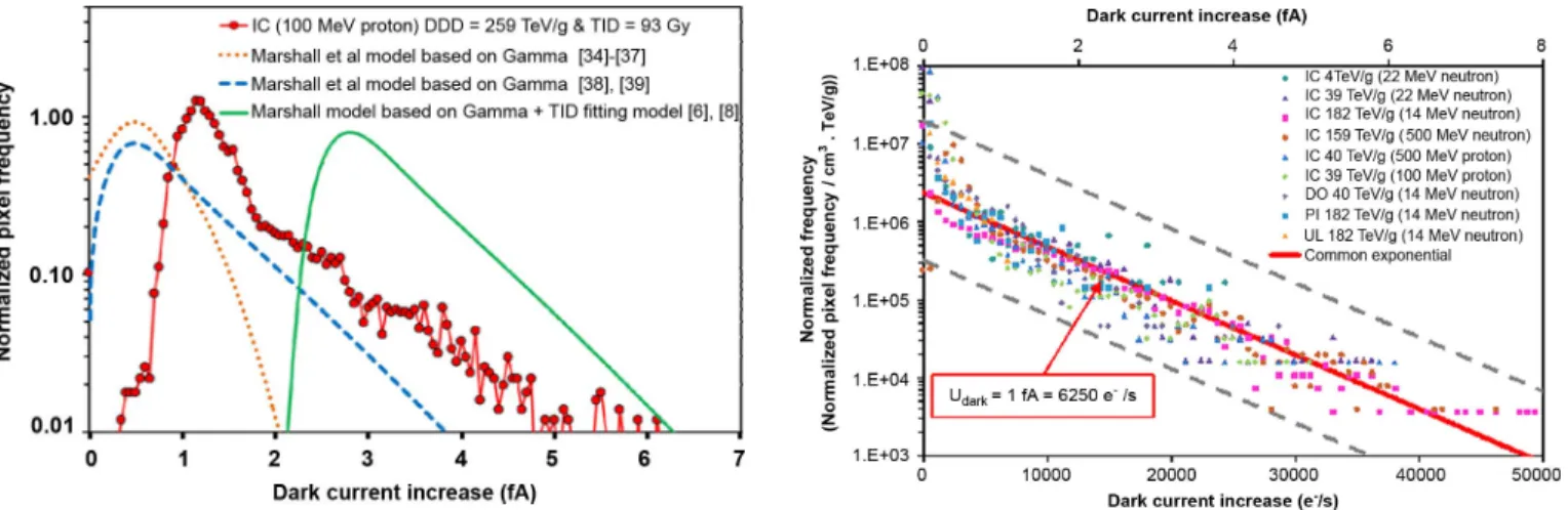
Fig. 7 presents the comparison between the physical model and experimental CIS results. We remind that no EFE param-eter [2] is taken into account, as we do not notice EFE in our devices (see Section III-C). The conversion factor used is 9.89 fA per MeV. This value is related to the UDF. The physical model using Gaussian clearly does not predict the current. Using Gamma distribution, the prediction is improved. The hot pixel tail of the experimental results seems to behave as the model. However the model underestimates the current in proton irradi-ated 3T-pixel CIS. We attribute this effect to the total ionizing dose which is not taken into account in the model. In order to add the TID contribution, we use the TID results obtained after -rays irradiate such 3T-pixel CIS [6], [8]. Assuming the inde-pendent contribution of interactions leading to TID and DDD, we performed the convolution of the physical model (large blue dashes) with TID fitting results. The model is also plotted in a green line in Fig. 7. This combined model overestimates the cur-rent. But, as TID results come from -rays irradiations on CIS bias during tests to replicate the worst in-flight case [38],
Fig. 7. Model of dark current increase distribution after 100 MeV proton irradi-ation. The experimental data are not very well modeled by the existing physical model.
[39], we suggest that the TID deposit during the 100 MeV proton irradiation without bias provides less damage. However, even if we reduce the impact of TID (which leads to a shift of the histogram to the lower dark current value), we observe that the model and the experimental distribution do not present exactly the same behavior for such irradiation. On the experimental histograms, there is always a break between the Gaussian part and the exponential tail, which is not present on the models. Therefore, the hypothesis about the independence of interac-tions leading to DDD and to TID should be examined.
This physical model correctly predicts dark current increases in CID and CCD imagers but it is not directly transposable to the CIS devices where a large contribution to the dark cur-rent comes from TID effect. Moreover this model is strongly time-consuming due to the calculation of the energy distribu-tion (especially if no tabulated data are available, i.e., for neu-trons). We note that the model compares the damage energy to the dark current, that means it includes all the defects created due to displacement damage and the defect scattering leading to stable electro-active defects generating the dark current.
Other approaches exist to model dark current increase in CIS. They are based on the fitting method of the cumulative dark cur-rent distribution [9], [10]. From these results, authors extract parameters proportional to the number or the activity of the de-fects and the density of the hot pixel tail. In these approaches, the considered distribution is not the dark current increase dis-tribution but the cumulative dark current disdis-tribution. There-fore, the dark current before and after irradiation is cumulated. This means that electro-active defect already present inside the sensor should be taken into account in their conclusions.
V. ENGINEERINGMODEL OF THEEXPONENTIALHOTPIXEL
DISTRIBUTION
A. Concept of a Unique Exponential Distribution
The existing physical model does not perfectly fit the dark current increase after proton irradiations in our 3T-pixel CIS and is difficult to adapt for neutron irradiations [12]. Therefore, based on all proton and neutron tests in the large number of
Fig. 8. Displacement damage induced exponential distribution of the dark cur-rent increase. The relative frequency is normalized by the number of pixels, the photodiode depleted volume and the displacement damage dose. All studied dis-tributions present the same exponential behavior. The mean of the exponential law, , is extracted. The value is .
investigated CIS, we proposed an alternative approach to an-alyze the hot pixel tails. This approach is based on two partic-ular observations. The first one is the common exponential be-havior observed in all CIS irradiated with protons and neutrons [1]–[12]. This common behavior could be due to a common electro-active distribution leading to dark current after displace-ment damage. The second concerns the UDF validity in tested CIS. This agreement with the UDF means that the dark current of the hot pixel tail due to displacement damage comes from bulk defects located in the space charge region of the in-pixel photodiode. This is confirmed using activation energy analysis. Moreover the dark current appears to be proportional to the dis-placement damage dose. Therefore, under these observations, we normalized the dark current increase distributions with the pixel depleted volume, the number of pixels and the displace-ment damage dose.
Fig. 8 illustrates the normalized distributions for 3T-pixel CIS and 4T-pixel CIS using a pinned photodiode. These devices are manufactured using different design and process. This means the depleted volume changed from one device to another. The results correspond to DDD less than 200 TeV/g. This maximum value is experimentally fixed to stay in the range of displace-ment damage interaction under one per pixel. The change of exponential behavior for higher doses will be discussed in the next part.
For all CIS, we observe a common exponential tail. The ex-ponential law is used to model the distributions:
(2) where corresponds to the mean value of the exponential law (that is to say the slope on the semi-logarithmic plot).
The value is equal to . We focus on
the hot pixel tail since the beginning of the dark current increase distribution combines TID and DDD contributions for proton ir-radiations. From this observation, we assume that an exponen-tial distribution of the hot pixel tail appears when few pixels are
Fig. 9. Probability density function of the dark current increase related to one interaction per pixel leading to electro-active defects. The mean value of the distribution , is equal to 1 fA.
impacted by displacement damage (i.e., when the probability to have more than one displacement damage interaction per pixel is low). We can deduce a probability density function (PDF) for this law. The dark current increase represented by it depends on the depleted volume and the DDD. This PDF is illustrated in Fig. 9. It represents the dark current distribution of the hot pixel tail. On the experimental CIS results, we note that this distri-bution is distorted when the dose increases above 200 TeV/g. That is to say, when a larger number of pixels is impacted by displacement damage the exponential behavior is changed, as we can see in Figs. 2 and 3. This is related to more than one displacement damage interaction per pixel occurring in a sig-nificant number of pixels. Therefore the DDD, the number of pixels and the depleted volume should be correlated to model the hot pixel tail of the dark current distributions.
B. Construction of the Dark Current Increase Distribution Model
In order to predict the dark current increase distribution, we assume that the dark current increase distribution is equal to the probability to have one defect due to displacement damage in-teraction per pixel, multiplied by the PDF related to one defect due to displacement damage interaction per pixel plus the prob-ability to have two defects multiplied by the convolution of the first PDF by itself, plus, etc.,
(3) For DDD under 200 TeV/g in our tested devices, we consider that the probability of having more than one defect is negligible. Therefore, (3) becomes:
(4) where is the distribution related to one defect due to displacement damage interaction. This PDF corresponds to the exponential law previously deduced using the experimental
Fig. 10. PDF exponential distribution with and its convolution by itself are used to build the exponential-based model. is used in this example.
measurements for DDD under 200 TeV/g. That is to say (2)
define .
For the highest DDD, we have to take into account the prob-ability of having more than one defect per pixel. As the number of defects due to displacement damage per pixel is weak, we choose the Poisson statistic to describe this probability:
(5) where is the number of defects per pixel due to displacement damage and the mean number of these defects.
The final distribution related to the dark current increase dis-tribution is defined as:
(6) Fig. 10 represents the exponential PDF using
and the n-fold convolution by itself to build the PDF for each number of defects. The largest dark line corresponds to the final model, (6), using . In order to illustrate this final model for several values, Fig. 11 is drawn. In this figure value ranges from 0.1 to 5. We clearly observed that for less than 1 (corresponding to low DDD), the model keeps the exponential behavior (the terms corresponding to more than one defect per pixel can be ignored) whereas for above one, the exponential behavior is distorted. This phenomenon is due to the convolu-tion of the exponential law by itself.
Then, this model is used to fit all the dark current increase distributions investigated. Therefore, for each distribution we obtained a parameter. As this parameter is related to the dis-placement damage dose and the depleted volume, we plot the parameter divided by the depleted volume against the displace-ment damage dose. This analysis is presented in Fig. 12. The results obtained in this figure show a correlation between the
Fig. 11. Construction of dark current increase PDF for several parameters.
Fig. 12. Relation between parameter normalized by photodiode depleted volume and the displacement damage dose. Proportionality between both pa-rameters seems to appear leading to another universal parameter . The
value of is around .
parameter with the DDD. Hence, the parameter can be ex-pressed:
(7) where corresponds to the factor between , the depleted volume and the dose. From experimental proton and neutron
re-sults, is equal to . This factor
is related to the quantity of electro-active defects induced by displacement damage in the pixel depleted volume.
We can include the factor deduced from (5) in the (4) to obtain the final engineering model based on an empirical anal-ysis of a large amount of CIS data. This model should be able to predict all the presented dark current increase distributions using solely a set of two factors, and (with fixed values). We remind that the model is deduced from experimental data obtained after proton and neutron irradiation.
VI. MODELING OF THEEXPERIMENTALDATA
A. Neutron Experimental Data
The engineering model described in the previous section is used to estimate dark current increase distributions. It is com-pared to the experimental measurements. The results of tron-irradiated CIS are plotted in Fig. 13 with the model. As
neu-Fig. 13. Experimental dark current increase after neutron irradiations and mod-eling calculation. The model agrees with experimental data.
Fig. 14. Experimental dark current increase after proton irradiations and mod-eling calculation. As explained previously, in case of proton irradiations, the peak of dark current increase under 2 fA is mainly attributed to TID. Displace-ment damage-induced dark current increase is observed above this value. There-fore, the model which is related to solely DDD, agrees with dark current increase above 2 fA (the hot pixel tail).
trons only provide displacement damage [12] the model agrees with the entire experimental data distribution and for the total range of DDD explored.
B. Proton Experimental Data
Fig. 14 compares the proton-induced dark current increase data and the model. As explained previously, protons provide additional interaction and TID which induced other dark cur-rent increase sources in 3T-pixel CIS. This effect is observed in Fig. 14, for low dark current increase, a peak appears mainly related to TID. However, the second part of the proton distribu-tions (the hot pixel tail) agrees well with the model.
VII. CONCLUSION
In this paper, the similarities between proton- and neutron-in-duced dark current increase distribution in CIS have been em-phasized. The mean dark current increase due to displacement damage appears to be proportional to the displacement damage dose in our large set of irradiated CIS. The universal damage factor is used to estimate the displacement contribution and we note that this factor could be used to predict the displacement damage in several types of CIS using conventional photodiodes (3T-pixel) and pinned photodiodes (4T-pixel). The dark current
distributions obtained after proton and neutron irradiations also show similarities, the hot pixel tail increases with the displace-ment damage dose and keeps an exponential behavior. A spe-cific normalization of these distributions using the in-pixel de-pleted volume and the displacement damage dose allows deduc-tion of a common effect of the hot pixel tail in all devices. Based on this observation, we propose an empirical model to estimate the dark current increase distributions in our CIS (3T-pixel and 4T-pixel) and for proton (ranging from 50 MeV to 500 MeV) and neutron (ranging from 14 MeV to 22 MeV) irradiations. This model is based on two factors which are fixed for all tested CIS. It could be interesting to validate this model on other sets of data using other technologies and other particle energies and fluences.
ACKNOWLEDGMENT
The authors would like to thank CIMI Group for their help, especially F. Corbière for the sensor conception, P. Cervantes and B. Avon for their help with measurements, S. Rolando and P. Martin-Gonthier for their critical point of view about the study. They would also thank TRIUMF’s Committee for pro-viding the proton beam time, S. Quenard, Y. Leo, CEA, Valduc, M. Boutillier, CNES and G. Berger, UCL, Belgium, for their as-sistance during neutron and proton irradiations.
REFERENCES
[1] G. R. Hopkinson, “Radiation effects in a CMOS active pixel sensor,” IEEE Trans. Nucl. Sci, vol. 47, no. 6, pp. 2480–2484, Dec. 2000. [2] J. Bogaerts, B. Dierickx, and G. Meynants, “Enhanced dark current
generation in proton-irradiated CMOS active pixel sensors,” IEEE Trans. Nucl. Sci, vol. 49, no. 3, pp. 1513–1521, Jun. 2002.
[3] J. Bogaerts, “Radiation-Induced Degradation Effects in CMOS Active Pixel Sensors and Design of Radiation-Tolerant Image Sensor,” Ph.D. dissertation, Katholieke Univ, Leuven, 2002.
[4] J. Bogaerts, B. Dierickx, G. Meynants, and D. Uwaerts, “Total dose and displacement damage effects in a radiation-hardened CMOS APS,” IEEE Trans. Electron Dev., vol. 50, no. 1, pp. 84–90, 2003. [5] G. R. Hopkinson, “Radiation effects on a radiation-tolerant CMOS
ac-tive pixel sensor,” IEEE Trans. Nucl. Sci, vol. 51, no. 5, pp. 2753–2762, Dec. 2004.
[6] V. Goiffon, “Contribution à une Approche Structure de la Conception des Imageurs CMOS en vue de Leur Durcissement à l’Environnement Radiatif Spatial,” Ph.D., ISAE, Univ. Toulouse, Toulouse, France, 2008.
[7] M. Innocent, “A radiation tolerant 4T pixel for space applications,” Proc. IISW, 2009.
[8] C. Virmontois, I. Djite, V. Goiffon, M. Estribeau, and P. Magnan, “Proton and -ray irradiation on deep sub-micron processed CMOS image sensor,” Proc. ISROS, pp. 217–222, 2009.
[9] M. Beaumel, D. Herve, and D. V. Aken, “Cobalt-60, proton and electron irradiation of a radiation-hardened active pixel sensor,” IEEE Trans. Nucl. Sci., vol. 57, no. 4, Aug. 2010.
[10] A. M. Chugg, R. Jones, M. J. Moutrie, J. R. Armstrong, D. B. S. King, and N. Moreau, “Single particle dark current spikes induced in CCDs by high energy neutrons,” IEEE Trans. Nucl. Sci., vol. 50, no. 6, pp. 2011–2017, 2003.
[11] M. Deveaux, G. Claus, G. Deptuch, W. Dulinski, Y. Gornushkin, and M. Winter, “Neutron radiation hardness of monolithic active pixel sen-sors for charged particle tracking,” Nucl. Instr. Meth. A, vol. 512, pp. 71–76, 2003.
[12] C. Virmontois, V. Goiffon, P. Magnan, S. Girard, C. Inguimbert, S. Petit, G. Rolland, and O. Saint-Pé, “Displacement damage effects due to neutron and proton irradiations on CMOS image sensors manufac-tured in deep sub-micron technology,” IEEE Trans. Nucl. Sci., vol. 57, no. 6, pp. 3101–3108, Dec. 2010.
[13] B. Hancock and G. Soli, “Total dose testing of a CMOS charged particle spectrometer,” IEEE Trans. Nucl. Sci., vol. 44, no. 6, pp. 1957–1964, Dec. 1997.
[14] E.-S. Eid, T. Y. Chan, E. R. Fossum, R. H. Tsai, R. Spagnuolo, J. Deily, W. B. Byers, and J. C. Peden, “Design and characterization of ionizing radiation-tolerant CMOS APS image sensors up to 30 mrd (Si) total dose,” IEEE Trans. Nucl. Sci., vol. 48, no. 6, pp. 1796–1806, Dec. 2001. [15] M. Cohen and J.-P. David, “Radiation-induced dark current in CMOS active pixel sensors,” IEEE Trans. Nucl. Sci, vol. 47, no. 6, pp. 2485–2491, Dec. 2000.
[16] B. Pain, B. R. Hancock, T. J. Cunningham, S. Seshadri, C. Sun, P. Pedadda, C. J. Wrigley, and R. C. Stirbl, “Hardening CMOS imagers: Radhard-by-design or radhard-by-foundry,” Proc. SPIE, vol. 5167, pp. 101–110, 2004.
[17] M. Deveaux, J. Berst, W. D. Boer, M. Caccia, G. Claus, G. Deptuch, W. Dulinski, G. Gaycken, D. Grandjean, L. Jungermann, J. Riester, and M. Winter, “Charge collection properties of X-ray irradiated monolithic active pixel sensors,” Nucl. Instr. Meth. A, vol. 552, pp. 118–123, 2005. [18] P. R. Rao, X. Wang, and A. J. P. Theuwissen, “Degradation of CMOS image sensors in deep-submicron technology due to -irradiation,” Solid-State Electron., vol. 52, no. 9, pp. 1407–1413, Sep. 2008. [19] V. Goiffon, P. Magnan, O. Saint-Pé, F. Bernard, and G. Rolland,
“Total dose evaluation of deep submicron CMOS imaging technology through elementary device and pixel array behavior analysis,” IEEE Trans. Nucl. Sci., vol. 55, no. 6, pp. 3494–3501, Dec. 2008. [20] V. Goiffon, M. Estibeau, and P. Magnan, “Overview of ionizing
ra-diation effects in image sensors fabricated in a deep-submicrometer CMOS imaging technology,” IEEE Trans. Electron. Dev., vol. 5, pp. 2594–2601, 2009.
[21] R. E. Coath, J. P. Crooks, A. Godbeer, M. D. Wilson, Z. Zhang, M. Stanitzki, M. Tyndel, and R. A. D. Turchetta, “A low noise pixel ar-chitecture for scientific CMOS monolithic active pixel sensors,” IEEE Trans. Nucl. Sci, vol. 57, no. 5, pp. 2490–2496, Oct. 2010.
[22] J. P. Carrere, J. P. Oddou, C. Richard, C. Jenny, M. Gatefait, S. Place, C. Aumont, A. Tournier, and F. Roy, “New mechanism of plasma induced damage on CMOS image sensor: Analysis and process optimization,” Solid-State Electron., vol. 65–66, pp. 51–56, Sep. 2010.
[23] J. Tan, B. Büttgen, and A. Theuwissen, “4T CMOS image sensor pixel degradation due to X-ray radiation,” presented at the Int. Image Sensor Workshop - IISW, 2011.
[24] J. R. Srour and D. H. Lo, “Universal damage factor for radiation-in-duced dark current in silicon devices,” IEEE Trans. Nucl. Sci, vol. 47, no. 6, pp. 2451–2459, Dec. 2000.
[25] G. Vincent, A. Chantre, and D. Bois, “Electric field effect on the thermal emission of traps in semiconductor junctions,” J. Appl. Phys., vol. 50, no. 8, pp. 5484–5487, Aug. 1979.
[26] N. Teranishi, A. Kohono, Y. Ishihara, E. Oda, and K. Arai, “No image lag photodiode structure in the interline CCD image sensor,” in IEDM Tech. Dig, Dec. 1982, vol. 28, pp. 324–327.
[27] P. Lee, R. Gee, M. Guidash, T. Lee, and E. R. Fossum, “An active pixel sensor fabricated using CMOS/CCD process technology,” in Proc. IEEE Workshop on CCDs and Advanced Image Sensors, 1995, pp. 115–119.
[28] A. J. P. Theuwissen, “CMOS image sensors: State-of-the-art,” Solid-State Elect., vol. 52, pp. 1401–1406, 2008.
[29] H. I. Kwon, I. M. Kang, B. G. Park, J. D. Lee, and S. S. Park, “The analysis of dark signals in the CMOS APS imagers from the character-ization of test structures,” IEEE Trans. Elec. Dev., vol. 51, no. 2, pp. 178–184, Feb. 2004.
[30] P. W. Marshall, C. J. Dale, E. A. Burke, G. P. Summers, and G. E. Bender, “Displacement damage extremes in silicon depletion regions,” IEEE Trans. Nucl. Sci., vol. 36, no. 6, pp. 1831–1839, Dec. 1989. [31] C. J. Dale, P. W. Marshall, and E. A. Burke, “Particle-induced spatial
dark current fluctuations in focal plane arrays,” IEEE Trans. Nucl. Sci, vol. 37, no. 6, pp. 1784–1791, Dec. 1990.
[32] P. W. Marshall, C. J. Dale, and E. A. Burke, “Proton-induced displace-ment damage distributions and extremes in silicon microvolumes,” IEEE Trans. Nucl. Sci., vol. 37, no. 6, pp. 1776–1783, Dec. 1990. [33] C. J. Dale, L. Chen, P. J. McNulty, P. W. Marshall, and E. A. Burke,
“A comparison of Monte Carlo and analytic treatments of displacement damage in Si microvolumes,” IEEE Trans. Nucl. Sci., vol. 41, no. 6, pp. 1974–1983, Dec. 1994.
[34] M. S. Robbins, “High-energy proton-induced dark signal in silicon charge coupled devices,” IEEE Trans. Nucl. Sci., vol. 47, no. 6, pp. 2473–2479, Dec. 2000.
[35] R. Germanicus, S. Barde, L. Dusseau, G. Rolland, C. Barillot, F. Saigné, R. Ecoffet, P. Calvel, J. Fesquet, and J. Gasiot, “Evalua-tion and predic“Evalua-tion of the degrada“Evalua-tion of a COTS CCD induced by displacement damage,” IEEE Trans. Nucl. Sci., vol. 49, no. 6, pp. 2830–2835, Dec. 2002.
[36] V. Goiffon, C. Virmontois, P. Magnan, S. Girard, and P. Paillet, “Anal-ysis of total dose induced dark current in CMOS image sensors from interface state and trapped charge density measurements,” IEEE Trans. Nucl. Sci., vol. 57, no. 6, pp. 3087–3094, Dec. 2010.
[37] T. Watanabe, J.-H. Park, S. Aoyama, K. Isobe, and S. Kawahito, “Ef-fects of negative-bias operation and optical stress on dark current in CMOS image sensors,” IEEE Trans. Electron Dev., vol. 57, no. 7, pp. 1512–1518, Jul. 2010.
[38] T. Oldham and F. B. McLean, “Total ionizing dose effects in MOS ox-ides and devices,” IEEE Trans. Nucl. Sci., vol. 50, no. 3, pp. 483–499, Jun. 2003.
[39] P. Paillet, J. R. Schwank, M. R. Shaneyfelt, V. ferlet-Cavrois, R. L. Jones, O. Flament, and E. W. Blackmore, “Comparison of charge yield in MOS devices for different radiation sources,” IEEE Trans. Nucl. Sci., vol. 49, no. 6, pp. 2656–2661, Dec. 2002.