HAL Id: hal-00960068
https://hal.archives-ouvertes.fr/hal-00960068
Submitted on 17 Mar 2014
HAL is a multi-disciplinary open access
archive for the deposit and dissemination of
sci-entific research documents, whether they are
pub-lished or not. The documents may come from
teaching and research institutions in France or
abroad, or from public or private research centers.
L’archive ouverte pluridisciplinaire HAL, est
destinée au dépôt et à la diffusion de documents
scientifiques de niveau recherche, publiés ou non,
émanant des établissements d’enseignement et de
recherche français ou étrangers, des laboratoires
publics ou privés.
Proposal and Design of an All-Optical Encoder for
Digitising Radio-over-Fibre Transceivers
Ricardo Ribeiro, Frédéric Lucarz, Bruno Fracasso
To cite this version:
Ricardo Ribeiro, Frédéric Lucarz, Bruno Fracasso. Proposal and Design of an All-Optical Encoder for
Digitising Radio-over-Fibre Transceivers. NOC 2013 : 18th European Conference on Networks and
Optical Communications ; OC&I 2013 : 8th Conference on Optical Cabling and Infrastructure, Jul
2013, Graz, Austria. �hal-00960068�
Proposal and Design of an All-Optical Encoder for
Digitising Radio-over-Fibre Transceivers
Ricardo M. Ribeiro
Departamento de Engenharia de Telecomunicações Universidade Federal Fluminense
24.210-240, Niterói, RJ - Brasil rmr@pq.cnpq.br
Frédéric Lucarz and Bruno Fracasso
Département d’ÓptiqueTélécom Bretagne 29280, Brest - France frederic.lucarz@telecom-bretagne.eu
Abstract—In this paper it is proposed and designed an
original all-optical Encoder (o-Encoder) intended, but not exclusively, to be part of future optical digitising radio-over-fibre (o-DRoF) transceiver. It is based on the Semiconductor Laser Amplifier Loop Mirror (SLALOM) configuration exploiting the nonlinearities of a semiconductor optical amplifier (SOA) in cross-switching regime. The proof-of-principle is established using 40-ps RZ control pulses at 2.5 GHz in the C-band. It outputs serially encoded, quantized and amplified optical RZ bits. Computer simulations of the proposed o-Encoder have shown promising results. The proposed device is rather compact, potentially optically integrable and requires much less input optical power (by several orders of magnitude) than other photonic-encoders and can also naturally convert wavelengths in the optical domain.
Keywords—analogue-digital conversion; encoder; microwave-photonics; optical signal processing; semiconductor optical amplifier
I. INTRODUCTION
Analogue Radio-over-Fibre (ARoF) is a key-technology for the convergence of fibre-based wireline and wireless networks [1]. ARoF allows a relatively simple distribution of RF signals over optical fibres connecting a Central Station (CS) to Base Stations (BSs) or Remote Antenna Units (RAUs). Therefore, all signal processing may be centrally carried out at the CS [1,2], leading to simple RAUs design that only needs to implement optoelectronic conversion and power amplification. However, ARoF systems are constrained by two basic requirements, which are inherent to analogue transmissions [1]: all used devices should be highly linear and the received signal should have higher SNR (Signal to Noise Ratio) than those obtained with digital systems.
In order to circumvent the limitations of ARoF networks, the use of digitised radio-over-fibre (DRoF) technologies [1-6] is an interesting alternative. In electronic DRoF links the analogue RF input signal is first digitised by an analogue-to-digital converter (ADC), the generated electrical bits drive a light source thus generating optical bits then transported over an optical fibre and finally are reconstructed by a digital-to-analogue converter (DAC) at the output of a photo-detector.
Each BS (or RAU) comprises one ADC and one DAC, while more complex digital signal processing is carried out in the CS [2]. Due to the digital nature of the optical link, the dynamic range is independent of the fibre length as long as the power of the received signal is lower than the link sensitivity. Electronic DRoF technologies still exhibit some advantages over ARoF [2,3] except for its relative higher complexity, but include further characteristics as follows: centralised digital signal processing such as digitisation itself, enhanced sharing capacity, better compatibility of digital equipments and communication channels, significant increase in transmission distance using optical fibre (larger dynamic range), larger coverage capacity or larger number of RAUs, possible cost reduction and energy saving.
The signal conversion and high-speed processing (including switching and routing) in the all-photonic domain are required for next-generation networks due to the accelerated growth of demanded traffic reaching Exabyte per month. All these processes when performed in the electronic domain require optical/electrical (O/E) conversion that introduces complexities and delays. Therefore, by using all-photonic DRoF more operations and signal processing centralisation at the CS would be achievable. The main challenges in the electronic DRoF link implementation are: high-speed ADC and DAC, dispersions, nonlinearities (in electrical and optical domains), additive noise, integration of system and devices, size and system cost.
An o-DRoF transmitter may comprise an RF interface circuit connected to an optical sampler, which is it connected to an all-optical encoder. Alternatively, if an analogue RoF signal is already available, the o-DRoF transmitter comprises the optical sampler and the all-optical encoder. After the encoder an additional circuit (thresholder) is generally needed in order to enhance the contrast between the optical bits [7].
To the best of our knowledge, no complete experimental
o-DRoF communication system has been reported in the
literature. However, some recently published papers [3-5] from Brunel University (UK) report valuable theoretical simulations of an o-DRoF system but without any detailed description of the operational principles of both all-optical ADC and DAC.
Ricardo M. Ribeiro thanks Foundation Capes/MEC-Brasil for the financial support through a Post-Doctoral fellowship under the grant BEX 9096/11-6.
At least, an optical ADC (o-ADC) should be able to optically sample the incoming analogue signal, to encode, to quantize and eventually to automatically amplify the output optical bits [4,7]. In this paper, we propose the use of chained optical circuits based on the SLALOM configuration in the cross-switched regime to provide an o-Encoder. Computer simulation results on VPI Transmission MakerTM software are presented for the 1550 nm wavelength window, 2.5 GHz repetition rate with 40-ps RZ control pulses. Since the proposed optical circuits use a laser amplifier as the nonlinear optical element, they may potentially perform additional functions, such as: wavelength conversion (present paper), data regeneration, clock recovery [8] and modulation format conversion [9]. The o-DRoF systems may well integrates into the next generation of all-photonic telecommunication networks [3-6] and provides the connection between the access and the metropolitan network or even the high-capacity transport networks.
II. ALL-OPTICAL DIGITISING RADIO-OVER-FIBRE
TRANSMITTER (O-DROF-T)
This section proposes an o-DRoF-T able to simultaneously perform signal digitisation and wavelength conversion in the optical domain. The transmitter essentially comprises an
o-ADC assuming the analogue RoF signal is already available.
Electronic ADC and DAC boards seem to exhibit an intrinsic limitation in their stability, “bit resolution x input frequency” product and data conversion rates of up to a few tenths of GSa/s [3-6,10].
Since the end of the 1970’s, the vast majority of all-optical ADC and DAC systems have always been separately reported and for various types of applications, but excluding any communication link application. To our knowledge, no complete experimental o-DRoF link system has ever been reported in the literature.
Figure 1 depicts a flowchart of the basic transmitter module architecture of an o-DRoF link [10,11] able to digitise RoF signals.
The o-DRoF-T comprises at least five main optical sub-modules: (1) optical pulse generator or o-Generator, (2) optical sampler or o-Sampler [12], (3’) and (3’’) temporal interleavers or o-Interleaver, (4) optical encoder or o-Encoder and (5) optical thresholder or Thresholder [7]. The
o-Sampler [12] carries out the optical sampling of an input
analogue RoF signal and is driven by an optical pulse comb that in turn is generated by the o-Generator. This pulse comb is also used as a reference clock signal by the o-Encoder that optically encodes the sampled signal, thereby accomplishing the photonic AD-conversion itself. The o-Thresholder [7] is provided mainly to significantly enhance the contrast between the “0” and “1” optical bits at the output of the o-Encoder and automatically providing amplification. The o-Generator is rather implemented by a mode-locked laser, a key component used to generate a series of picoseconds pulses at GHz rates with high temporal stability, i.e. with very low jitter in the femtoseconds time-scale [10,11]. Therefore, these pulses can
be used as the clock signal for the optical sampling and encoding steps. The interleavers (3’) and (3’’) essentially multiply the repetition rate of the clock signal generated by the
o-Generator (1) as is explained further in section III.B.
Fig. 1. The flowchart of the basic o-DRoF-T. The o-Encoder sub-module treated is this paper is highlighted and numbered as (4).
III. THE OPERATIONAL PRINCIPLE OF THE O-ENCODER
A. General
Sagnac interferometric fibre rings have been used as a nonlinear device based on self-phase modulation (SPM) or cross-phase modulation (XPM) – Nonlinear Optical Loop Mirrors (NOLMs) – that are very useful for many ultrafast signal-processing applications [10,13]. However, for fibre lengths greater than a few hundred meters, the stability of the NOLM is significantly degraded. Furthermore, the long fibre introduces excessive latency for some optical processing applications [14].
The use of a laser amplifier as a nonlinear medium instead of the optical fibre leads to an interesting class of devices usually named as SLALOM [15] or Terahertz Optical Asymmetric Demultiplexer (TOAD) [16] depending on application.
The optical circuits of the Sampler, Interleaver,
o-Encoder and o-Thresholder were designed and simulated
using VPI Transmission MakerTM software. However, in this paper only the results for the o-Encoder are presented. All circuits were probed at 1550 nm wavelength window with 2.5 GHz repetition rate (5.0 Gbit/s), 20-ps time-width RZ pulse stream (40-ps for the control pulses). The peak power (Pcontrol) of the control pulses could be varied from few µW to mW in order to obtain the transfer function, i.e. the Poutput x Pcontrol curves.
The input probe and control pulses at 1554.0 nm and 1562.1 nm wavelengths, respectively, were both generated from a continuous-wave laser diode with null linewidth after traversing a Mach-Zehnder modulator (MZM). The MZM is
biased at the quadrature point and is driven by 5.0 Gbit/s RZ electrical pulses in an alternate pattern with 0.1 or 0.05 duty-cycle.
The optical circuits of the Encoder, Sampler and
o-Thresholder [7] are Sagnac interferometers using
fibre-couplers with a coupling ratio equal to 50:50, thus allowing a maximum interference visibility contrast. The insertion of an attenuator (passive component) in the Sagnac fibre ring provides the breaking of reciprocity and an increase in optical power equalisation between the clockwise (CW) and counter-clockwise (CCW) pulses. This is because there are different amplifying gains. The SOA is modelled as to be isotropic. The CW and CCW pulses polarisation are assumed to be always aligned. The polarisation alignment can be achieved in practice by using polarisation controllers in the optical circuits or by using polarisation-maintaining fibres.
B. The o-Interleaver
Figure 2 shows the proposed fibre-optic circuit of the
o-Interleavers (3’) and (3’’) suitable for 3-bits resolution.
The circuit uses four 3-dB fibre-couplers (FC), two delay lines and two variable optical attenuators (Att). By appropriately setting the attenuations and the delays, it is possible to generate three temporally interleaved pulses from each sampled pulse. Such three pulses frame may presents either required pattern of peak power. As will be explained ahead, such a pattern as the one generated by the (3’)
o-Interleaver is needed to correctly operate the o-Encoder. The
(3’’) o-Interleaver is setting with Att1 = Att2 = 0-dB attenuation thus producing interleaved pulses with the same amplitude.
Fig. 2. The general fibre-optic circuit of the o-Interleavers suitable for 3-bits resolution.
Each sampled pulse generated by the o-Sampler [12] sub-module at sampling frequency fS is processed by the
o-Interleaver (3’), thus producing three temporally interleaved
pulses at 3fS repetition frequency. The most intense of these pulses will present P3 peak power, while the second will present P2 =P3/2. For an ideal transfer function (following (1)) the amplitude of the first (weaker) pulse would be P1 = P2/2 = P3/4.
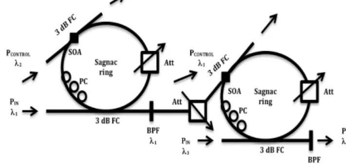
C. The chained o-Encoders
Figure 3 shows two chained nonlinear Sagnac fibre-interferometers where the transmitted output of the first ring after traversing an optical attenuator, is launched in the second
fibre ring as to be the control light. The chain may be extended to contain three or more Sagnac rings following the same pattern.
Fig. 3. The general fibre-optic circuit of two chained o-Encoders.
The transfer function of an ideal Sagnac interferometer is given by (1). € PT1 = PIN 1 2
[
1− cos Δφ(
)
]
(1) In (1), PIN,€
P
T 1, and Δφ represent respectively the input peak power, transmitted peak power and the differential phase-shift between the CW and CCW pulses. The differential phase-shift depends on the optical nonlinear strength γ, the length LSOA of the SOA inserted in the ring and the control power (peak) PC.as given by (2).
€
Δφ= 2γLSOAPC (2)
The SOA inserted in the Sagnac ring is an active element and the output signal will be optically amplified, i.e. PT > PIN and usually PT > PC. Therefore, an optical attenuator (of α attenuation) should be inserted between each pair of Sagnac rings in order to fit the amplitude of the control pulses at PT/α, in such a way that (PT)max/α = (PIN)max. As a result, the output
€
P
T2 from the second Sagnac ring is given by (3).
€ PT 2 = PIN 1 2 1− cos 2γLSOA PT 1 α (3) After inserting (2) in (1) and then substituting the resulting equation in (3), one obtains the response (transfer function) of the two cross-chained Sagnac rings as given by (4).
€ PT 2 = PIN 1 2 1− cos 2 γ αLSOAPIN 1 2
[
1− cos 2(
γLSOAPC)
]
(4) Figure 4 shows comparatively the plots of 1-stage and 2-stage chained o-Encoders based on an ideal Sagnac fibre-optic interferometer.The 1-stage transfer function reaches Δφmax = 2π and is suitable for 2-bit resolution (see the explanation accompanying Figure 6 and reference [10]). The 2-stage transfer function can reach Δφmax = 4π using the same peak power of the control light. One extra bit resolution is achieved for each o-Encoder stage added in the circuit of Figure 3.
Fig. 4. The plots of the 1-stage (Δφmax = 2π) – 2-bits – and 2-stage – 3-bits – transfer function o-Encoders based on an ideal Sagnac fibre-optic interferometer.
Figure 5 shows comparatively the plots of 1-stage and 2-stage chained o-Encoders based on an ideal Sagnac fibre interferometer, but now starting with Δφmax = 4π (1-stage).
Fig. 5. The plots of the 1-stage (Δφmax = 4π) – 3-bits – and 2-stage – 5-bits – transfer function o-Encoders based on an ideal Sagnac fibre interferometer.
The 1-stage transfer function now reaches Δφmax = 4π and is suitable for 3-bit resolution (see Figure 6 and reference [10]). However, the 2-stage transfer function now can reaches Δφmax = 16π using the same peak power of the control light. Now, two extra bit resolution is achieved for each o-Encoder stage added in the circuit of Figure 3.
Figure 6 reproduces the 2-stage plot of Figure 4 (Δφmax = 2π) and illustrates the process of digital coding using the (2-stage) o-Encoder able to provide the Gray-code with 3-bits resolution [10,17].
In order to enable the 3-bit resolution, the threshold level is placed at ~20% of the maximum transmitted power instead of the conventional 50% [10]. The abscissa of Figure 6 is sectioned in eight (23-bit =8) “slots” of the same width. As an
example of generation of the digital Gray-code, assume an optical sample of P3 = 5.86 rad amplitude that lies in the middle of the rightmost “slot”. The circuit of Figure 2 when properly set is able to generate interleaved pulse replicas with P2 = P3/2 = 2.93 rad and P1 = P2/2 = 1.47 rad. By simply inspecting Figure 6, P1, P2 and P3 corresponds to “1”, “0” and “0” bits, respectively, i.e. the “100” sequence. Now, following the reasoning and starting with P3 = 5.09 rad that lies in the middle of the next “slot”, P2 = 2.55 rad and P3 = 1.27 rad are generated by the o-Interleaver circuit. The “101” digital code sequence is now generated. The remaining Gray-code sequences may be generated unambiguously in the same way. The same procedure may be performed for the 2-stage transfer function suitable for 5-bit resolution as shown in Figure 5. A simple inspection shows that the cycles are steeper and the threshold level should be placed at < 20% of the maximum transmitted power.
Fig. 6. The transfer function plot of the 2-stage o-Encoders illustrating the process of generation of the Gray-code based optical bits with 3-bits resolution. An ideal Sagnac fibre interferometer is assumed. The threshold level is the dotted horizontal line placed at ~20% of the maximum transmitted power.
It is a relatively difficult task to obtain an ideal transfer function even using optical fibres as the nonlinear optical element [10]. The deviation from (1) is usually more severe when a SOA is used instead of an optical fibre (see section IV).
D. The o-Thresholder
The o-Thresholder based on the use of SOA as the nonlinear optical element is described in details in reference [7]. Figure 7 depicts the general fibre-optic circuit of the proposed o-Thresholder operating in self-switching regime.
The typical transfer function of the o-Thresholder [7] resembles that of the laser diode. From Pinput = 0 to a threshold Pinput = Pth input power, the device is able to practically block the transmitted output light. This is because Pinput is very low and the differential phase-shift is not enough to produce significant switching from the reflection to the transmission port of the interferometer. From Pinput = Pth to Pinput = Plim input power, the device presents a transition region thus reaching a
limited output power for Pinput > Plim. The limiting region is achieved due to saturation of available carriers thus significantly decreasing the self-phase modulation strength when the input light power continues to increase. All characteristic powers and speed of the o-Thresholder transfer function may be tuned once the circuit parameters are properly set, e.g. attenuation Att, bias current IDC of the SOA and the asymmetry x.
Fig. 7. The general fibre-optic circuit of the o-Thresholder.
IV. MODELLING AND SIMULATIONS OF THE O-ENCODER Figure 3 depicts the fibre-optic circuit design of the 1-stage and 2-stage o-Encoder. The physical model solves the nonlinear Schrödinger equation (NLSE) taking into account the SPM and XPM effects in the bulk and isotropic SOA as an active nonlinear waveguide. The model assumes a SOA with low feedback and uses the Transmission Line Model (TLM) to compute the differential nonlinear phase-shift induced by a change in carrier density in the semiconductor. As a result, the switching is driven by the XPM effect occurring into the SOA. Table I shows the 2-stage o-Encoder parameters as used in the computer simulations.
Figure 8 shows the result of the computer simulation of the 1-stage and 2-stage o-Encoder circuit of Figure 3 using LSOA = 500 µm, IDC = 200 mA and 12 dB attenuation between the circuits.
It should be observed that the real control peak power is the half of those shown in the abscissa of Figure 8 (and of Figure 9). The reason is because a conventional 3 dB fibre-optic coupler is used instead of a WDM-coupler to launch the control power in the SOA (see Figure 3).
The 1-stage transfer function achieved is highly asymmetric. Only Pπ ~ 60 µW is needed to achieve a complete switching, i.e. from Δφ = 0 to Δφ = π rad, while P2π ~ 230 µW is needed to reach Δφ = 2π rad. A ratio of P2π/ Pπ = 2.00 should be presented by a symmetric transfer function, but the P2π/ Pπ = 230/60 = 3.83 ratio was really achieved. One reason behind this asymmetry is the fact that the SOA is operating in a non-saturated regime where the non-linearity is very strong and highly dependent on the number of carriers. When the control power is increased the number of available carriers decreases and the non-linearity strength also decreases. Therefore, more power (> 60 µW) is needed for
switching from Δφ = π to Δφ = 2π. The consequence of such asymmetry is seen in the 2-stage transfer function plot also shown in Figure 8. Although, the transfer function still presents two cycles as in the ideal o-Encoder of Figures 4 and 6, now it is no longer possible to unambiguously generate the Gray-code digital sequences.
Figure 9 shows the result of the computer simulation of the 1-stage o-Encoder circuit of Figure 3 using LSOA = 300 µm and IDC = 250 mA. Now, Pπ ~ 275 µW is needed to achieve a complete switching, while P2π ~ 675 µW. The P2π/ Pπ = 675/275 = 2.45 ratio was achieved meaning that the transfer function is now reasonably closer to the symmetric shape when compared with Figure 8. Because the LSOA is reduced from 500 to 300 µm, the nonlinear optical effects are weaker since Pπ and P2π are both increased, even taking into account that the IDC is increased from 200 to 250 mA. The choice of 12 dB attenuation between the stages of chained o-Encoder is because the 7.25 mW maximum power transmitted from the first circuit should be reduced to reach 460 µW (before the 3dB fibre-coupler) maximum as is required for Δφ = 2π rad.
Fig. 8. Simulations of the transfer function as designed with 1-stage and 2-stage chained o-Encoders fibre-optic circuit using 12 dB attenuation, LSOA = 500 µm and IDC = 200 mA.
Fig. 9. Simulations of the transfer function as designed with 1-stage
o-Encoder fibre-optic circuit for LSOA = 300 µm and IDC = 250 mA. The asymmetry is reduced.
The SOA itself is a relatively complex device to be designed, even though specific SOAs intended to optical signal processing are already available in the market. It should be treated not only as an optical amplifier but also as a nonlinear waveguide where the control and probe pulses are propagating and interacting with each other. Its dynamics of operation is not trivial. When the SOA is placed in a fibre-optic Sagnac ring (see Figure 3) and control and probe light is launched, the 1-stage or 2-stage o-Encoder has to be even more complex to be properly designed. Besides those parameters which are adjusted here, many others can (or should be) simultaneously be taken into account such as wavelengths of the control and probe pulses, asymmetry of the SOA in the Sagnac ring, the use of a continuous wave holding beam [18] to obtain gain saturation and faster nonlinearities, semiconductor structure and length of the SOA, etc.
According to section III, since at least a symmetric transfer
function of (Δφ)max = 2π rad (one cycle) using 1-stage
o-Encoder is achieved, it turns out to be possible to reach 2-bit,
3-bit, 4-bit,…(n+1)-bit resolution by using 1, 2, 3,…n chained o-Encoders as the scheme of Figure 3. Nevertheless, if a symmetric transfer function of (Δφ)max = 4π rad (two cycles) using 1-stage o-Encoder could be achieved, now it turns out to be possible to reach 3-bit, 5-bit, 7-bit,…(2n+1)-bit resolution by using 1, 2, 3,…n chained o-Encoders. Therefore, the bit resolution is highly enhanced. It should be noted that the bit resolution is increased by increasing the number of “o-Encoder links” and the speed can be maintained fast if the Pout x Pcontrol response of each “link” is bounded to (Δφ)max = 2π, i.e. with reduced optical nonlinear effect (XPM) strength.
For the sake of simplicity, the 2-stage plot of Figure 8 was calculated with the same control and probe wavelengths as were used in the 1-stage simulation.
V. CONCLUSIONS
To the best of our knowledge, neither experimental nor commercially available o-DRoF links or networks have been reported as they are still under R&D stage. This paper proposes a transmitter module comprising at least five optical sub-modules for use in an o-DRoF link. It was designed and simulated here only the o-Encoder sub-module operating at 1550 nm wavelength window. The proposed chained
o-Encoders when compared with similar devices built using
fibre as an nonlinear optical element [10] may provide some advantages: compactness, prone to optical integration, requirement of ~103 less optical power and amplified output optical bits. D. Cotter et al also describe the implementation of a SLALOM circuit on a single 1x2 mm InP semiconductor chip [14] that supports the possibility of optical integration of the proposed o-DRoF-T.
In this paper, the simulations were constrained to only 2.5 GHz & 40-ps RZ input control pulses mainly to demonstrate the proof-of-principle of the o-Encoder. However, SOAs operating at 80 Gb/s are already commercially available [19]. Furthermore, SOAs in R&D stage able to operate up to 160 Gb/s [20] and beyond [21] have already been reported.
Simulations and experiments of the chained o-Encoders operating at higher pulse rate with shorter timewidth, other independent sub-modules of the proposed o-DRoF-T as well such transmitter as a whole are currently planned or in progress and will be presented in a near future.
ACKNOWLEDGMENT
Ricardo M. Ribeiro thanks the team at Département d’Optique of Telecom Bretagne and the CapilRTM platform for hosting his Post-Doctoral study during which the present work was carried out. The authors also thank INCT-Fotonicom/CNPq.
REFERENCES
[1] R. C. Williamson and R. D. Esman, RF Photonics, IEEE Journal of Lightwave Technology, Vol. 26, No. 9, 2008, pp. 1145-1151.
[2] A. Nirmalathas et al, Digitized Radio-Over-Fiber Technologies for
Converged Optical Wireless Access Network, IEEE Journal of
Lightwave Technology, Vol. 28, No. 16, 2010, pp. 2366 –2375. [3] S. R. Abdollahi, H. S. Al-Raweshidy and R. Nilavalan, Fully-Photonic
Analogue-to-Digital Conversion Technique for Super-Broadband Digitized-Radio over Fibre Link, 16th European Conference on Networks and Optical Communications, Newcastle, UK, July 20-22, 2011, pp. 72-75.
[4] S. R. Abdollahi et al, Digital Radio over Fibre for Future Broadband
Wireless Access Network Solution, 6th International Conference on Wireless and Mobile Communication, Valencia, Spain, September 20-25, 2010.
[5] S. R. Abdollahi et al, Non-Uniform Wavelength Allocation in
All-Photonic Digitized-Radio over Fibre Access Network, 14th International Symposium on Wireless Personal Multimedia Communications, Brest, France, October, 2011.
[6] A. Viglienzoni and H. Al-Raweshidy, Net! Works - Next Generation
Network: Wireless-Optics Technology, European Technology Platform,
White Paper, June 06, 2011.
[7] R. M. Ribeiro, F. Lucarz and B. Fracasso, A Thresholder for All-Optical
Digitising Radio-over-Fibre Transceivers, 17th Conference on Optical Network Design & Modeling (ONDM 2013), Brest, France, April 16-19, 2013, pp.160-165.
[8] I. D. Phillips et al, Simultaneous demultiplexing, data regeneration, and
clock recovery with a single semiconductor optical amplifier-based nonlinear-optical loop mirror, Optics Letters, Vol. 22, No. 17, 1997, pp.
1326-1328.
[9] X. Yang et al, Application of Semiconductor Optical Amplifiers in
High-Speed All-Optical NRZ to RZ Format Conversion, ICTON 2007, Paper
We.D2.3, 2007, pp. 228-231.
[10] Y. Miyoshi et al, All-Optical Analog-to-Digital Conversion Using
Split-and-Delay Technique, IEEE Journal of Lightwave Technology, Vol. 25,
No. 6, 2007, pp. 1339-1347.
[11] M. Currie, High-Performance Photonic Analog-to-Digital Converter
and Low-Noise Mode-Locked Fiber Laser, U.S. Navy, Final Report,
NRL/MR/5650--03-8679, May 26, 2003.
[12] R. M. Ribeiro, F. Lucarz and B. Fracasso, An All-Optical Sampler for
Digitising Radio-over-Fibre Transceivers, 18th European Conference on Network & Optical Communications (NOC 2013), July 10-12, Graz, Austria, 2013, in press.
[13] G. Huang et al, All-Optical OOK to 16-QAM Modulation Format
Conversion Employing Nonlinear Optical Loop Mirror, IEEE Journal of
Lightwave Technology, Vol. 30, No. 9, 2012, pp. 1342-1350.
[14] D. Cotter et al, Nonlinear Optics for High-Speed Digital Information
Processing, Science, Vol. 286, 1999, pp. 1523-1528.
[15] M. Eiselt, Optical Loop Mirror with Semiconductor Laser Amplifier, Electronics Letters, Vol. 28, No. 16, 1992, pp. 1505-1507.
[16] J. P. Sokoloff et al, A Terahertz Optical Asymmetric Demultiplexer
(TOAD), IEEE Photonics Technology Letters, Vol. 5, No. 7, 1993, pp.
787-790.
[17] H. F. Taylor, An Optical Analog-to-Digital Converter—Design and
Analysis, IEEE Journal of Quantum Electronics, Vol. QE-15, No. 4,
1979, pp. 210-216.
[18] R. J. Manning and D. A. O. Davies, Three-wavelength device for
all-optical signal processing, Optics Letters, Vol. 19, No. 12, 1994, pp.
889-891.
[19] 1550 nm Nonlinear SOA from Amphotonix, www.kamelian.com. [20] K. Szuki et al, Error-free demultiplexing of 160 Gbit/s pulse signal
using optical loop mirror including semiconductor laser amplifier,
Electronics Letters, Vol. 30, No. 18, 1994, pp. 1501-1503.
[21] Y. Liu et al, Error-Free 320-Gb/s All-Optical Wavelength Conversion
Using a Single Semiconductor Optical Amplifier, IEEE Journal of
![Figure 1 depicts a flowchart of the basic transmitter module architecture of an o-DRoF link [10,11] able to digitise RoF signals](https://thumb-eu.123doks.com/thumbv2/123doknet/12518603.341687/3.892.487.823.171.460/figure-depicts-flowchart-transmitter-module-architecture-digitise-signals.webp)