HAL Id: hal-03034438
https://hal.archives-ouvertes.fr/hal-03034438
Submitted on 3 Dec 2020HAL is a multi-disciplinary open access
archive for the deposit and dissemination of sci-entific research documents, whether they are pub-lished or not. The documents may come from teaching and research institutions in France or abroad, or from public or private research centers.
L’archive ouverte pluridisciplinaire HAL, est destinée au dépôt et à la diffusion de documents scientifiques de niveau recherche, publiés ou non, émanant des établissements d’enseignement et de recherche français ou étrangers, des laboratoires publics ou privés.
Buffer layers inhomogeneity and coupling with epitaxial
graphene unravelled by Raman scattering and graphene
peeling
Tianlin Wang, Jean-Roch Huntzinger, Maxime Bayle, Christophe Roblin,
Jean-Manuel Decams, Ahmed-Azmi Zahab, Sylvie Contreras, Matthieu
Paillet, Périne Landois
To cite this version:
Tianlin Wang, Jean-Roch Huntzinger, Maxime Bayle, Christophe Roblin, Jean-Manuel Decams, et al.. Buffer layers inhomogeneity and coupling with epitaxial graphene unravelled by Raman scattering and graphene peeling. Carbon, 2020, 163, pp.224-233. �10.1016/j.carbon.2020.03.027�. �hal-03034438�
1
Buffer layers inhomogeneity and coupling with
epitaxial graphene unravelled by Raman
scattering and graphene peeling
Tianlin Wang1, Jean-Roch Huntzinger1, Maxime Bayle1,!, Christophe Roblin1, Jean-Manuel
Decams2, Ahmed-Azmi Zahab1, Sylvie Contreras1, Matthieu Paillet1 and Périne Landois1,*
1 Laboratoire Charles Coulomb, UMR 221, Univ Montpellier, CNRS, Montpellier, France 2 Annealsys, 139 rue des Walkyries, 34000 Montpellier, France
! present address : Institut des Matériaux Jean Rouxel, UMR 6502 CNRS/Université de Nantes 2, rue de
la Houssinière, BP 32229, 44322 Nantes Cedex 3, France
* corresponding author. Tel: 0033467144138. E-mail: perine.landois@umontpellier.fr;
Abstract
The so-called buffer layer (BL) is a carbon rich reconstructed layer formed during SiC (0001) sublimation. The covalent bonds between some carbon atoms in this layer and underlying silicon atoms makes it different from epitaxial graphene. We report a systematical and statistical investigation of the BL signature and its coupling with epitaxial graphene by Raman spectroscopy. Three different BLs are studied: bare buffer layer obtained by direct growth (BL0), interfacial buffer layer between graphene and SiC (c-BL1)
and the interfacial buffer layer without graphene above (u-BL1). To obtain the latter, we develop a
mechanical exfoliation of graphene by removing an epoxy-based resin or nickel layer. The BLs are ordered-like on the whole BL growth temperature range. BL0 Raman signature may vary from sample to
sample but forms patches on the same terrace. u-BL1 share similar properties with BL0, albeit with more
variability. These BLs have a strikingly larger overall intensity than BL with graphene on top. The signal high frequency side onset upshifts upon graphene coverage, unexplainable by a simple strain effect. Two fine peaks (1235, 1360 cm-1), present for epitaxial monolayer and absent for BL and transferred graphene. These findings point to a coupling between graphene and BL.
2
1. Introduction
Epitaxial graphene (EG) grown on silicon carbide (SiC) by sublimation has been considered as one of the most promising candidates for the graphene-based nanoelectronic device fabrication. Especially in the field of metrology, the EG-based resistance standard has already been largely developed in a decade [1– 3]. The accessibility of wafer-scale and high-quality graphene films achieved by sublimation on Si-face of SiC (0001) under argon (Ar) pressure is one of the major advantages of this growth method [4–6]. During the high temperature annealing, the SiC surface undergoes several reconstructions phases before graphene formation [7–12]. The carbon-rich reconstructed layer on top of SiC(0001) is well known as buffer layer (BL). The BL is a layer of carbon atoms arranged in a honeycomb structure with partially sp3 hybridization [10,13–15]. Based on the X-ray photoelectron spectroscopy (XPS) results, about 1/3 of the carbon atoms are covalently bonded to the silicon atoms of the SiC substrate, leading to the partial sp3 hybridization in BL which differs from sp2 graphene layer [11,13]. We name BL
0 the first BL to grow.
Further sublimation generates a new carbon layer at the interface of the previous BL and the SiC substrate [16]. Meanwhile, the previous BL detaches from the substrate and converts into the first graphene layer. The new carbon layer is the interfacial BL (named BL1) which is always present underneath graphene in
SiC (0001) sublimation.
In the literature, there is an intense debate about the BL atomic structure. Several BL structures have been proposed and investigated theoretically [17,18]. The scanning tunneling microscopy (STM) images commonly show a (6 × 6) structure of BL which do not agree with the low-energy electron diffraction (LEED) patterns showing a 6√3 × 6√3𝑅30° reconstruction [7–12]. According to the calculation of S. Kim et al. [19], the (6 × 6) structure in STM images is the result of the atomic corrugations due to the presence of underlying BL and from the weak electronic interaction between EG and BL. Furthermore, the early XPS studies have estimated that about 1/3 of carbon atoms in BL are covalently bonded to the substrate [10,13] while the recent study of Conrad et al. [20] have suggested that this ratio is no more than 26%. Regarding the electrical properties, angle-resolved photoelectron spectroscopy (ARPES) measurement highlighted that the existing covalent bonds suppress the 𝜋 bands of graphene. The early results showed a wide gap insulator characteristic of BL [11,13] while the picture changed recently and found the BL to be a small gap semiconductor [21,22].
Raman spectroscopy is largely used to study the structural and electronic properties of carbon structure [23–27]. Several works have shown the Raman spectra of bare buffer layer (BL0) which is the first carbon
layer formed without topmost graphene growth (Fig. 1a). Different types of have been reported, with two main broad peaks [28–30] or with three main peaks [6,31–34]. Although the discrepancies of these
3
reported spectra are significant, there is still no systematic and statistical analysis aiming to understand this disagreement.
Besides BL0, it is widely accepted that the interfacial BL (graphene covered BL, c-BL1, Fig. 1b) which
is situated between graphene and the substrate has an important influence on the topmost EG in terms of electronic and structural properties of grown graphene. The intrinsic n-type doping observed in EG has been explained by the electrons transfer between the BL and SiC substrate [11,13]. Furthermore, the strain effect of BL on EG has been evidenced by grazing incidence X-ray diffraction measurement [30]. These mentioned substrate influences on EG have been supported by a post-growth hydrogen intercalation treatment which can saturate the bonds between substrate and BL, converting the latter into real graphene layer [11,35]. The influence of graphene on BL was considered in a former Raman analysis, where a decrease in Raman integrated intensity of BL, with a ratio of 3 after the growth of EG, was observed [28]. An open question remained, whether the difference in integrated intensity is due to the graphene overlayer presence or due to a difference in growth environment. For instance, the BL1 forms with a carbon layer
above and the growth temperature of BL0 and BL1 are different. Thus, there still remains considerable
work to understand and control this graphene/SiC (0001) interface structure.
This work is a systematic and statistic investigation of the BL signature and its interaction with topmost graphene using Raman spectroscopy. The first buffer layer (BL0) is investigated in section 3.1. Then to
determine whether the reduction in buffer signal discussed above is due to the mere presence of graphene, we develop a peeling technique to mechanically remove the graphene layer from c-BL1 in section 3.2.1.
This technique, illustrated in figure 1c, exposes the now uncovered BL1 (u-BL1) without topmost
graphene. This u-BL1 is compared to BL0 in section 3.2.2. Finally, both non-covered buffers (BL0 and
u-BL1) are compared to covered BL1 (c-BL1) in section 3.2.3.
Figure 1: Schematic illustration of three types of BLs: (a) bare buffer layer BL0, (b) still covered interfacial
buffer layer (c-BL1) [NB: in terms of samples, “1LG” and “c-BL1” are one and the same] and (c)
4
2. Experimental details
The studied samples were grown on 6 mm × 6 mm, on-axis, semi-insulating 4H-SiC (0001), cut from a 3 inch Tankeblue wafer and epi-ready polished on the Si-face by NovaSiC. SiC (0001) sublimation was conducted in an Annealsys Zenith-100, a high temperature RTP (Rapid Thermal Processing) - CVD furnace. During the entire sample growth process, we kept a low argon pressure (10 mbar, 800 sccm) in the chamber. The annealing temperature is ranged between 1600 and 1740°C for BL0 investigations, and
fixed at 1750°C for monolayer EG samples, including those used to analyze the BL1. The dwell time was
300 s unless stated explicitly. More details of the furnace system and sample preparation process were presented in our early work [6].
The mechanical peeling of graphene has been performed on our EG samples. This exfoliation process is illustrated in figure 2. On the pristine sample image, the terrace edges are clearly visible (Fig. 2a). In a first step, an epoxy-based resin (M-bond 610) or Ni film has been deposited on the whole sample surface (Fig. 2b). Then, due to the higher binding energy between resin (or Ni, less than 50 nm thick) and graphene compared to that between graphene and BL [36,37], by pulling the handling layer, graphene can be mechanically peeled (Fig. 2c). The handling layer is either a microscope coverslip for M-bond 610 or a thermal release tape for Ni. Therefore, only uncovered buffer (u-BL1) was left on the SiC substrate while
the graphene layer was transferred onto the deposited thin epoxy-based resin or Ni film (Fig. 2d). Both the SiC and the resin substrates have higher refractive index than air, so that graphene appears brighter on the optical image in reflection mode. The graphene on the central terrace in the red ellipse failed to be transferred. Indeed, graphene is missing in the darker corresponding area in the resin image. This image is mostly bright, an indication that the peeling process is rather efficient.
5
Figure 2: Graphene peeling process. Schematic cross section and optical images at different stages: (a) pristine sample with covered buffer (c-BL1), (b) after resin or Ni deposition, (c) handling layer addition
on top to mechanically remove resin (or Ni) and graphene layers and (d) resulting pieces: left, uncovered buffer on SiC (u-BL1) and right, transferred graphene (t-1LG) on resin or Ni layer. To ease images
comparison, a mirror operation was applied to the last image, and a black arrow and a red ellipse were overlaid.
Raman spectra and maps were recorded using an Acton spectrometer fitted with a Pylon CCD detector and a 600 grooves/mm grating (~2.5 cm-1 between CCD pixels). The samples were excited with a 532 nm
(2.33 eV) laser line (Millennia Prime, Newport) through a ×100 objective (numerical aperture 0.9, Olympus). The full width at half-maximum (FWHM) of the focused laser spot is about 400 nm. Optimized focus conditions were checked for each measurement. The samples were mounted on a three-axis piezoelectric stage (Physik Instrumente) to ensure the precise positioning and focusing of the laser spot. A HOPG (Highly Oriented Pyrolytic Graphite) sample was used as a daily reference for the system calibration. Laser power was continuously measured during acquisitions allowing intensity normalizations
6
of the Raman spectra and maps. We have developed three distinct home-made Labview software dedicated to repositioning, acquisition and analysis. The first one, combined to optical microscopy and piezoelectric stage allowed a repeated imaging of the same area, with a micrometric precision. For instance, it enables to study the same location before and after the graphene peeling experiment. The second one controlled the whole experimental setup. Finally, all data were analyzed using the third one. In particular, graphene or BL Raman spectra have been obtained by subtracting the Raman spectrum of the bare SiC substrate (see supplement, Part A). We note that the individual spectra and integrated intensity calculated for certain spectral region were normalized by dividing the value of the integrated intensity of G-peak (𝑨𝑮) by the one of the corresponding HOPG reference (𝑨𝑮𝑯𝑶𝑷𝑮) allowing the comparison between spectra or maps made at different times:
𝑨𝑮𝒏𝒐𝒓𝒎= 𝑨𝑮⁄𝑨𝑮𝑯𝑶𝑷𝑮
3. Results and discussion
We investigate here first the characteristics of the direct growth buffer (BL0) in part 3.1. The graphene
peeling results are described in part 3.2.1, then the Raman responses of BLs without graphene on top, BL0
and the uncovered buffer (u-BL1), are compared in part 3.2.2. Finally, the comparison is extended to the
graphene covered BL, the c-BL1, in part 3.2.3.
3.1 Inhomogeneity of bare buffer layer (BL0)
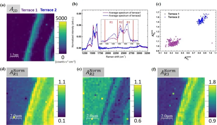
Figure 3a shows the Raman A2D map collected from a direct growth BL0 sample (sample DG1, zone A
- DG stands for Direct Growth). By comparison with the corresponding optical and AFM images (Fig. S9) and analyzing the Raman data, we identify two graphene ribbons located close to step edges and BL0 on
two SiC terraces. We denote the left and right terraces as terrace 1 and terrace 2, respectively. Their representative average spectra are shown in figure 3b. These two average spectra collected from two neighboring terraces are significantly different. Noticeably, the broad peaks situated close to 1390 cm-1
and 1620 cm-1 have higher intensity on terrace 2 than on terrace 1.
In the literature, BL signature is usually fitted by Gaussian functions [6,31,32]. These Gaussians are very broad and their physical meaning is not clear, especially for the contribution centered about 1550 cm
7
All spectra presented two dips almost at the same position. So, we have chosen to divide this range in three regions: i) 1260 to 1460 cm-1; ii) 1460 to 1550 cm -1; iii) 1550 to 1710 cm-1, denoted as R1, R2 and R3 (inset image of Fig. 3b) and to use their numerically integrated intensities as metrics to capture the differences in the measured spectra. This method presents several advantages. Three simple integrations are faster than a fit with 4 Gaussians. Moreover, the integration is clear and straightforward while the fit can be sensitive to initial parameters. The integrated areas of each region, AR1, AR2 and AR3 were
normalized by integrated intensity of the monolayer graphene taken as 𝐴𝐺,𝑚𝑜𝑛𝑜 = 0.03 𝐴𝐺,𝐻𝑂𝑃𝐺 [38] and indicated as 𝐴𝑅𝑛𝑜𝑟𝑚𝑖 in figures 3 and 4.
To give more statistical details, points of the Raman map corresponding to BL (A2D < 150 counts s -1 cm-1 in figure 3a; see sup. info. part C for the detailed justification for this criteria) are plotted in 𝐴
𝑅1
𝑛𝑜𝑟𝑚
and 𝐴𝑅𝑛𝑜𝑟𝑚3 coordinates (Fig. 3c). Points from terrace 1 and 2 are displayed as open purple and solid blue Figure 3: Raman analysis of sample DG1. (a) Raman A2D map. Navy-blue areas correspond to BL0 on two
terraces, while green areas correspond to EG. (b) Average spectra of terrace 1 (purple) and terrace 2 (blue). Inset: zoom between 1200 and 1800 cm-1. The vertical bars at 1260, 1460, 1550 and 1710 cm-1 delimit the 3 regions R1, R2 and R3 used in our analysis. (c) Relationship between 𝐴𝑅𝑛𝑜𝑟𝑚1 and 𝐴𝑅𝑛𝑜𝑟𝑚3 for the two terraces. (d-f) Raman 𝐴𝑛𝑜𝑟𝑚𝑅1 , 𝐴𝑅𝑛𝑜𝑟𝑚2 and 𝐴𝑅𝑛𝑜𝑟𝑚3 maps.
8
circles, respectively. Points from a given terrace are bunched together which confirms that the average spectra in figure 3b are relevant. On terrace 2 both 𝐴𝑅𝑛𝑜𝑟𝑚1 and 𝐴𝑅𝑛𝑜𝑟𝑚3 are higher than on terrace 1. These results demonstrate that the BL Raman signature can be very different even on the same sample as further illustrated by 𝐴𝑅𝑛𝑜𝑟𝑚1 , 𝐴𝑅𝑛𝑜𝑟𝑚2 and 𝐴𝑛𝑜𝑟𝑚𝑅3 in figure 3 (d-f).
This striking difference deserved an extended investigation summarized in figure 4. In figure 4a, we completed figure 3c, adding results of another zone of sample DG1 (zone B) and of samples DG2, DG3, DG4 and DG5. We note that, each studied areas, spanned more than one terrace. In addition, we found that both 𝐴𝑅𝑛𝑜𝑟𝑚1 and 𝐴𝑛𝑜𝑟𝑚𝑅3 , values acquired from one single terrace are relatively homogeneous, evidenced by a narrow distribution.
These scatter plots, varying with different terraces of a same sample and with different samples, confirmed an inhomogeneous Raman signature of BL0. For instance, 𝐴𝑅𝑛𝑜𝑟𝑚1 varies by more than a 2.5
factor. Moreover, figure 4a indicates a strong correlation between 𝐴𝑅𝑛𝑜𝑟𝑚1 and 𝐴𝑅𝑛𝑜𝑟𝑚3 . We found no such clear correlation between 𝐴𝑅𝑛𝑜𝑟𝑚2 and either 𝐴𝑛𝑜𝑟𝑚𝑅1 or 𝐴𝑅𝑛𝑜𝑟𝑚3 (Fig. S11).
These direct growth samples were synthesized at different growth temperatures ranging from 1600 to 1740°C (see table1). Samples DG2 (light yellow open circles) and DG3 (black open circles), synthesized at different temperatures, present similar 𝐴𝑅𝑛𝑜𝑟𝑚1 and 𝐴𝑅𝑛𝑜𝑟𝑚3 . Moreover, the two terraces of DG1 form Figure 4: (a) Relationship between 𝐴𝑛𝑜𝑟𝑚𝑅1 and 𝐴𝑅𝑛𝑜𝑟𝑚3 of BL0 samples synthesized at temperature
between 1600 and 1740°C. (b) Individual Raman spectra of selected BL0 points (BL signal without any
9
extremely separated clouds in figure 4a although they pertain to the same sample area. Hence, the growth temperature cannot be the direct cause of the inhomogeneity of our BL Raman signature.
Samples name DG1 DG2 DG3 DG4 DG5
Temperature growth (°C) 1740 1700 1650 1640 1600
Dwell (s) 10 300 300 300 300
Ramp (°C/s) 0.5 0.33 0.33 0.33 0.33 Table1: BL0 samples growth temperature (no peeling).
In the literature, a wide range of spectra have been reported for the BL from very disordered-like [28– 30,39] to more ordered-like [20,31,34,40,41] as in the present work.
Ordered-like BL can be viewed as a graphene layer sharing some sp3 bonds with the substrate. This might be why our buffer spectra share some similarities with sp3 functionalized graphene where modes localized nearby the sp3 defects have been identified [42]. They found modes attributed to sp3 atoms vibration in the same spectral range as our R1 region. Others modes in the 1300-1600 cm-1 range could be sp2 chains vibrations around the sp3 atoms, similar to their calculated CB-CC and CC-CD modes in [42].
But more theoretical investigations are required to check whether that applies to the BL.
To the best of our knowledge, the only few Raman analysis with extensive statistics were obtained on disordered-like BL [28,29]. Usually, only one or few spectra are presented in the literature. The progressive evolution from disordered-like to more ordered-like Raman spectra with increasing temperature has been reported by Kruskopf et al. [32]. Their carbon source was a polymer layer deposited on SiC prior to growth rather than SiC sublimation. Our results are thus hardly comparable. The temperature effect has also been considered by Conrad et al. [43]. These authors report that their B0, equivalent to R2 in our work (middle peak), reaches “a maximum at a growth temperature of 1414°C” [43].
To check this statement, we have synthesized BL0 samples varying the growth temperature from 1600
to 1740°C with a 10°C step (with fixed dwell time at 300 s and ramp at 0.33°C/s). The corresponding individual spectra are presented in figure 4b and show very similar lineshapes. This is at odd with the observation of Conrad et al. [43] that as the growth temperature is increased the Raman peak around 1490 cm-1 “initially increases and then appears suppressed once monolayer begins to form”. In our case, this peak never disappears although the spectra in figure 4b and figure S11 span the whole BL0 growth
range. Indeed, at 1600°C, it is difficult to find BL0 areas, as the sample is mostly bare SiC. At about
10
sample is almost fully covered with graphene. We have noted some imperfections in the subtraction method used in Ref. [43] as indicated by negative value of Raman intensity around the wavenumber of 1500 cm-1 in the presented spectra which might explain part of this discrepancy. More likely and given the large variations within a very same sample that we have highlighted above, it is insufficient to use single spectra to capture the characteristics of a sample. We can thus not clearly state at this stage whether the results presented in Ref. [43] are truly different from ours or not.
To summarize, we did not find any correlation between temperature and 𝐴𝑅𝑛𝑜𝑟𝑚1 , 𝐴𝑅𝑛𝑜𝑟𝑚2 or 𝐴𝑅𝑛𝑜𝑟𝑚3 . The inhomogeneity of the BL0 has thus another origin that still needs to be determined. Interestingly, Rutter et
al. found “two energetically stable configurations for the first carbon layer, depending on the initial graphene-SiC distance prior to full relaxation of the atomic coordinates” [44]. More recently, Cavalluci et al. have shown theoretically that several BL structures could have similar formation energies and “might appear in different experimental conditions or in different areas of the sample” [18]. They used a cubic polytype SiC in their calculations but 3C-SiC is “perfectly equivalent to 4H and 6H-SiC provided the SiC surface is planar” [17] and thus their results can be applied in our case (4H samples). Further work is needed to check whether this is indeed the explanation for the observed inhomogeneities in the BL Raman signature.
3.2 Comparison between buffer layers
In the previous section, we have shown the variability of the Raman signature of direct growth BL called BL0 above. Another puzzling result is the reduction of the BL overall intensity when it is covered with
graphene as already noticed in refs [28,43]. A buffer layer covered with monolayer graphene is the second carbon layer to be formed. It means that BL0 (the former BL) has been converted to graphene while a new
BL (called BL1) is formed underneath. There is no reason to assume a priori the very same structure for
BL0 and BL1, it is thus worth comparing the Raman signature of these two BLs. To enable such a
comparison, we use a peeling procedure to remove graphene from the top of BL1 and achieve uncovered
BL1 (u-BL1) samples. The results of the graphene peeling procedure are described hereafter in section
3.2.1. We focus on the comparison between the BL0 and u-BL1 Raman signatures, in section 3.2.2. The
influence of graphene on top of BL1 on the BL Raman signature will be discussed in the last section 3.2.3.
3.2.1 Graphene peeling
Figure 5a shows the Raman map (975 spectra) of the 2D-peak integrated intensity (denoted as A2D map)
11
detected in all the spectra, signifying a full coverage of the sample by graphene or few layer graphene. Besides, we found some broad features between 1200 and 1800 cm-1 close to the G-peak region which
could be identified as BL1 signature [6,28,31,32]. Two distinct areas can be identified in this A2D map:
green zones and yellow ribbons. We estimate the number of graphene layers from the corresponding 𝐴𝐺𝑛𝑜𝑟𝑚 ratio [6,38]. For spectra in green areas, the 𝐴𝐺𝑛𝑜𝑟𝑚 ratio ranges from 0.025 to 0.044 (402 spectra) in a Gaussian distribution centered at 0.033. This value indicates that most of the spectra in green areas could be attributed to monolayer graphene (1LG). On the other hand, the spectra in yellow areas possess an 𝐴𝐺𝑛𝑜𝑟𝑚 ratio ranging from 0.044 to 0.063, close to the expected value for 2LG (0.06). These 2LG stripes are localized at the step edges as commonly observed in EG due to the step-flow growth mode [4,45,46]. The average spectra of these two types of areas are presented in figure 5b as green and yellow spectra, respectively.
12
Figure 5c is the A2D map (1305 spectra) of this sample after the graphene peeling experiment. We
emphasize that this Raman map was recorded at the same place as the one in figure 5a. The intersection area is outlined by the dashed white rectangle in each map. In figure 5d, we average all spectra in the green/yellow areas (corresponding to about A2D > 2800 counts.s-1.cm-1) where we observe G-, 2D- peaks
and broad features between 1200 cm-1 and 1800 cm-1, indicating the presence of graphene and interfacial
c-BL1. We observe that the 2D signal dropped to quasi-zero value (A2D < 150 counts.s-1.cm-1, navy-blue
areas) in some areas. The average spectrum of all these areas where A2D is lower than 150 counts. s-1.cm -1 (see supplement part C for the detailed justification for this criteria) is shown as the navy-blue curve in
figure 5d. Thus, comparing these two A2D maps shown in figures 5a and 5c, the graphene flakes have
Figure 5: Raman analysis of a sample on which we have performed a graphene peeling. Two Raman A2D
maps (a) before and (c) after the graphene peeling (in counts.s-1.cm-1). The dashed white rectangles mark the common area of these two maps. Different representative domains have been indicated as BL, 1LG, 2LG and EG. Figures (b) and (d) show the average spectrum of each domain. The scanning steps of both x and y directions are 0.25 "μm"
13
probably been mechanically removed by the graphene peeling experiment, leaving in the previously identified areas the uncovered BL1 on the SiC surface. Meanwhile, we ignore all the spectra with A2D
between 150 and 2800 counts.s-1.cm-1, considering they could originate from a mixture of BL and EG. As expected, the well-defined G-peak and 2D-peak are absent in the navy-blue average spectrum but several intense and broad bands in the spectral region of 1200 – 1800 cm-1 have been revealed. Besides, a few low-intensity bumps extending from 2600 cm-1 to 3000 cm-1 are visible. Furthermore, this spectrum shares a similar lineshape with BL0 spectra, for instance in figures 3b and 4b. Moreover, these spectra are
comparable to BL Raman signature reported in litterature [6,29,31,47]. The successful graphene peeling exposed the now uncovered BL which will be compared to the BL0 in the next section.
3.2.2 Comparison between noncovered buffers (BL0 and u-BL1)
For the analysis of u-BL1 spectra, we use the same procedure as described is section 3.1 with the 3 regions denoted as R1, R2 and R3. Figure 6 includes the data obtained on BL0 and u-BL1 and displays
correlations between 𝐴𝑛𝑜𝑟𝑚𝑅1 and 𝐴𝑅𝑛𝑜𝑟𝑚3 (the 𝐴𝑛𝑜𝑟𝑚𝑅2 relationship with 𝐴𝑅𝑛𝑜𝑟𝑚1 or 𝐴𝑅𝑛𝑜𝑟𝑚3 is less clear as seen in figures S11a and S11b). Pink squares are for sample u-BL1-1 achieved by graphene peeling via Ni film
deposition method. The other squares correspond to maps at different areas of the sample u-BL1-2,
obtained by epoxy-based resin film deposition method. The main observation made out of this comparison is that 𝐴𝑛𝑜𝑟𝑚𝑅1 and 𝐴𝑅𝑛𝑜𝑟𝑚3 display a wider variation in these u-BL samples compared to each BL0 areas
(open circles). This variation occurs even in a single terrace such as for the olive-colored squares collected Figure 6: Correlation between 𝐴𝑛𝑜𝑟𝑚𝑅1 and 𝐴𝑅𝑛𝑜𝑟𝑚3 as figure 4a (BL0, open circles) with the addition of
14
on a 3𝜇𝑚 × 3𝜇𝑚 area of a single terrace. In other words, the data collected from a single u-BL1 terrace
show a larger distribution than one collected on any BL0 single terrace analyzed so far.
3.2.3 Comparison between buffer layer under graphene (c-BL1) and noncovered buffer layers (BL0 and u-BL1)
In the previous part, we showed that u-BL1 single terrace data are more scattered than on BL0. The
question to address is thus if that is a property of the second grown BL (BL1). Because of the
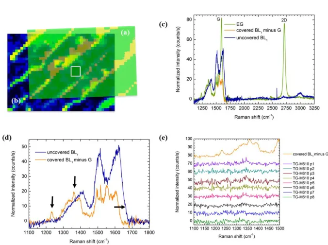
inhomogeneity of the BL described before, we need to compare data before and after graphene peeling acquired on the exact same area. Two superimposed Raman A2D maps of sample surface before and after
the graphene peeling are shown in figure 7a and b, respectively. Based on the previous analyses (section 3.2.1), we identify the green areas in map (a) as c-BL1 and navy-blue areas in map (b) as u-BL1. The
position of the after-peeling map has been unambiguously matched to the before-peeling map thanks to prominent features such as step edges and remaining graphene patches. To give spectral details with high signal to noise ratio, we average Raman spectra over a small area, checking that the average spectrum is representative of all the individual spectra of this area. Hence, the before and after spectra are genuine and not altered by any inhomogeneity. For instance, the average spectra of figure 7c come from the area outlined by a white solid square where graphene was successfully peeled off (9 spectra). The same was reproduced on other areas of the same sample and on 4 other samples with similar results.
To extract the BL1 contribution in the frequency region between 1200 cm-1 and 1800 cm-1, we subtracted
the G peak contribution in the EG (with BL underneath) spectrum. The residual is denoted as “covered BL1 minus G” in figure 7c. Figure 7d is a zoom on the 1100 cm-1 1800 cm-1 range. The following features
have been consistently observed on all the studied samples (see supplement, Fig. S15).
i) In the literature [20,28], it was observed that the “covered BL1 minus G” signal is smaller than BL0.
We observe the same trend in overall intensity (see supplement Fig. S13). The largest value of total integrated intensity of “covered BL1 minus G” of all the samples in this study is still smaller than the
15
The absorption of light by graphene can be estimated and is by far insufficient to explain the attenuation of the signal. A simple difference in the quantity of matter (buffer coverage, for example) without structural modifications can also be ruled out because of the strong changes observed in the spectra lineshape.
Figure 7: Superimposed Raman A2D maps (a) before and (b) after graphene peeling. (c) Average Raman
spectra of EG (green) and u-BL1 (navy-blue), respectively. The orange spectrum results from subtracting
a monolayer G-peak from the EG spectrum. All these spectra are averaged over the white square area in (a) and (b). (d) Zoom on the 1100-1800 cm-1 range. The vertical arrows mark the two fine peaks at about 1233 and 1363 cm-1. The horizontal arrow indicates the spectral upshift after graphene peeling. (e) Comparison between the EG spectrum and spectra of the graphene layer that was transferred on epoxy-based resin during the process described in 3.2.a. The spectra were collected from several well separated points at locations in and out of the white square common to (a) and (b) maps. More details are given in supplement part F (Fig. S14).
16
As another explanation, the topmost SiC layer might be partially converted to a new BL. This partial conversion would be a possible explanation for the Si depletion observed by Emery et al. [48] with only 25% of C atoms sp3 bonded to Si while other authors [11,13] observed the 33% expected for the standard 6√3 × 6√3𝑅30° reconstruction. In our case, the conversion would have to be more advanced in the BL0
samples (higher overall intensity) than in the BL1 samples. We propose to peel the top layer graphene (as
described in section 3.2.1). The signal after peeling should be close to “covered BL1 minus G”.
The results are surprising; the integrated intensity of the BL1 contribution considerably increases after the
peeling of the monolayer graphene, as visible in figure 7d and confirmed with more statistics in figures S12 and S13. The layers underneath the BL1 are exactly the same in both cases, since we were able to
compare the same part of the same sample before and after peeling. Hence, this experiment clearly rules out the partial conversion hypothesis.
Another possible origin for the difference between BL0 (the first grown BL) and “covered BL1 minus G”
(the second grown BL) could be a structural difference [43]. For instance, Schumann et al. [30] measured different lattice parameters for these two layers. Peeling is not expected to break the C-Si sp3 bonds between buffer and SiC because van der Waals coupling between buffer and graphene is much weaker than covalent bonds. But several structures could have similar energies. Then, it is not impossible that the former BL0 (that will become graphene) stabilized the BL1 growth underneath in a particular structure and
that the peeling process induced structural changes by rearranging the sp3 bonding. That would perhaps explain the large scatter in R1, R2 and R3 observed after peeling (Fig. 6 and Fig. S12). But it is not clear whether the mechanical energy developed during the peeling process is enough to overcome the relevant potential barrier.
The intensity change is more probably due to the coupling with graphene (when still covered) as already mentioned in a former work [28]. The exact mechanism is still to be found. It could be related to the corrugation of BL and graphene [16] that has been shown experimentally to be higher for BL0 than for
1LG surface [49] and might be partly attributed to smoother BL1 [30] as confirmed by Conrad et al. [43].
ii) After the graphene removal, the BL1 signal onset upshifts by 8 cm-1 as indicated by the horizontal
arrow in figure 7d. It would be tempting to attribute this shift to a strain relaxation. Indeed the graphene is compressively strained as usual on the Si-face of SiC [30,50]. Reciprocally, graphene would exert an expansive stress on the buffer. Further experiments detailed in supplement part G indicate that on the contrary, the graphene strain state plays no role in the buffer shift (Fig. S15 et S16). Hence, this shift is perhaps not due to a simple mechanical coupling between graphene and buffer. This seems reasonable since the van der Waals forces are weaker than the sp3 bonding between buffer and SiC. Another
17
possibility could be some screening phenomenon or charge transfer effect. That would require an extensive DFT calculations, outside the scope of this experimental paper.
iii) Two fine peaks at about 1235 cm-1 and 1360 cm-1 are observed in the “covered BL1 minus G”
spectra, indicated by vertical arrows in figure 7d. These two peaks are present on covered buffer (c-BL1)
spectra but absent in both noncovered BL1 (Fig. 5b and Fig. 7d) and BL0 (Fig. 3b, Fig. 5b and Fig. 7d).
They are also absent on the graphene that has been peeled by the resin (Fig. 7e). It should be stressed that, as shown in figure 7d, the peaks are absent in spectra coming precisely from the graphene layer that was probed in the figure 7a map where these peaks were initially present. Hence, graphene and buffer have to be in contact for these peaks to appear.
Kruskopf et al. [32] have observed similar peaks at about 1235 cm-1 and 1365 cm-1 and they attributed them to the vibrational density of states of the BL and the D-related peak, respectively, following Fromm et al. [51]. Rejhon et al. attributed the peak observed at 1237 cm-1 to “the LO/LA phonon branches at the Γ point” of the BL [41].
Since these peaks disappeared after peeling, they are not a pure property of the BL alone. Other explanations are possible. The low frequency peak could arise from a superlattice effect [52,53]. The peak near 1365 cm-1 could be similar to the D-like peak described by Gupta et al. [54]. In both cases, going further would require an extensive investigation with, for example, different excitation wavelengths.
4. Summary
We carried out an extensive study of the Raman signature of different kind of buffer layers (BLs), namely: BL0 the first grown (direct growth) buffer layer; c-BL1 the second grown buffer layer (BL1) which
is covered by graphene and finally u-BL1 uncovered BL1, which is obtained by post-growth mechanical
removal of the covering graphene. Special care was taken in the data acquisition, processing and analysis especially regarding the sample repositioning under the microscopes, the mandatory subtraction of the bare SiC substrate Raman spectrum and intensities normalization.
The whole BL growth temperature range has been investigated. After thorough cleaning of the furnace, only ordered-like BL (3 main peaks) was formed. Hence disordered-like BL (2 broad peaks) probably require another carbon source [32].
The BL0 Raman features in the 1200-1700 cm-1 range present important intensity variations not only
between different samples but even on different SiC terraces of a very same sample. Such changes are shown not to be correlated to the sample growth temperature contrary to what has been previously suggested [43]. Moreover, a clear correlation is found between the integrated intensities in the
1260-18
1460 cm-1 and 1550-1710 cm-1 regions. These results could be the signature of the coexistence of different
BL structures which can have close formation energies as evidenced by the theoretical work of Cavalluci et al. [18], but the structure and Raman signature relationship still remains to be established.
The graphene peeling technique developed and applied in this work allows the comparison of the two kinds of buffers without graphene on top: BL0 and u-BL1. We have shown that both Raman signatures
share similar properties although the u-BL1 samples exhibit larger distributions in terms of Raman
intensities.
Thanks to the graphene peeling technique and the sample repositioning method, we compare the Raman fingerprint of the exact same buffer layer with and without graphene above (c-BL1 vs. u-BL1). The results
revealed that the buffer layer contribution would increase after the graphene removal by showing a higher Raman integrated intensity. We believe this is a direct evidence of coupling between graphene and buffer layer. In the meantime, the signal onset at about 1600 cm-1 upshifts upon graphene coverage. These evolutions could be plausibly related to changes in the buffer layer, yet unexplained; however a simple strain effect between graphene and buffer layer has been ruled out. Furthermore, two fine peaks situated at 1235 and 1360 cm-1 are present in epitaxial monolayer spectrum while absent in that of buffer layer and transferred graphene, which might be interface coupling related.
All our findings point to a coupling between graphene and buffer layer. The origin of this coupling is still to be determined. We hope that these results will stimulate theoretical investigations that seem mandatory to gain further insight.
Acknowledgements
The WSxM software has been used to generate Raman map and AFM figures [55]. We thank Olivier Renault from CEA-LETI for XPS preliminary results.
References
[1] Lafont F, Ribeiro-Palau R, Kazazis D, Michon A, Couturaud O, Consejo C, et al. Quantum Hall resistance standards from graphene grown by chemical vapour deposition on silicon carbide. Nat Commun 2015;6:6806. https://doi.org/10.1038/ncomms7806.
[2] Ribeiro-Palau R, Lafont F, Brun-Picard J, Kazazis D, Michon A, Cheynis F, et al. Quantum Hall resistance standard in graphene devices under relaxed experimental conditions. Nature Nanotechnology 2015;10:965.
[3] Alexander-Webber JA, Huang J, Maude DK, Janssen TJBM, Tzalenchuk A, Antonov V, et al. Giant quantum Hall plateaus generated by charge transfer in epitaxial graphene. Sci Rep 2016;6:30296. https://doi.org/10.1038/srep30296.
[4] Emtsev KV, Bostwick A, Horn K, Jobst J, Kellogg GL, Ley L, et al. Towards wafer-size graphene layers by atmospheric pressure graphitization of silicon carbide. Nature Materials 2009;8:203.
19
[5] Virojanadara C, Syväjarvi M, Yakimova R, Johansson LI, Zakharov AA, Balasubramanian T. Homogeneous large-area graphene layer growth on 6 H -SiC(0001). Phys Rev B 2008;78:245403. https://doi.org/10.1103/PhysRevB.78.245403.
[6] Landois P, Wang T, Nachawaty A, Bayle M, Decams J-M, Desrat W, et al. Growth of low doped monolayer graphene on SiC(0001) via sublimation at low argon pressure. Phys Chem Chem Phys 2017;19:15833–41. https://doi.org/10.1039/C7CP01012E.
[7] Van Bommel AJ, Crombeen JE, Van Tooren A. LEED and Auger electron observations of the SiC(0001) surface. Surface Science 1975;48:463–72. https://doi.org/10.1016/0039-6028(75)90419-7.
[8] Forbeaux I, Themlin J-M, Debever J-M. Heteroepitaxial graphite on 6 H − SiC ( 0001 ) : Interface formation through conduction-band electronic structure. Phys Rev B 1998;58:16396–406. https://doi.org/10.1103/PhysRevB.58.16396.
[9] Chen W, Xu H, Liu L, Gao X, Qi D, Peng G, et al. Atomic structure of the 6H–SiC(0001) nanomesh. Surface Science 2005;596:176–86. https://doi.org/10.1016/j.susc.2005.09.013.
[10] Riedl C, Starke U, Bernhardt J, Franke M, Heinz K. Structural properties of the graphene-SiC(0001) interface as a key for the preparation of homogeneous large-terrace graphene surfaces. Phys Rev B 2007;76:245406. https://doi.org/10.1103/PhysRevB.76.245406.
[11] Riedl C, Coletti C, Starke U. Structural and electronic properties of epitaxial graphene on SiC(0 0 0 1): a review of growth, characterization, transfer doping and hydrogen intercalation. J Phys D: Appl Phys 2010;43:374009. https://doi.org/10.1088/0022-3727/43/37/374009.
[12] Srivastava N, He G, Luxmi, Mende PC, Feenstra RM, Sun Y. Graphene formed on SiC under various environments: comparison of Si-face and C-face. J Phys D: Appl Phys 2012;45:154001. https://doi.org/10.1088/0022-3727/45/15/154001.
[13] Emtsev KV, Speck F, Seyller Th, Ley L, Riley JD. Interaction, growth, and ordering of epitaxial graphene on SiC{0001} surfaces: A comparative photoelectron spectroscopy study. Phys Rev B 2008;77:155303. https://doi.org/10.1103/PhysRevB.77.155303.
[14] Varchon F, Feng R, Hass J, Li X, Nguyen BN, Naud C, et al. Electronic Structure of Epitaxial Graphene Layers on SiC: Effect of the Substrate. Phys Rev Lett 2007;99:126805. https://doi.org/10.1103/PhysRevLett.99.126805.
[15] Goler S, Coletti C, Piazza V, Pingue P, Colangelo F, Pellegrini V, et al. Revealing the atomic structure of the buffer layer between SiC(0001) and epitaxial graphene. Carbon 2013;51:249–54. https://doi.org/10.1016/j.carbon.2012.08.050.
[16] Varchon F, Mallet P, Veuillen J-Y, Magaud L. Ripples in epitaxial graphene on the Si-terminated SiC(0001) surface. Phys Rev B 2008;77:235412. https://doi.org/10.1103/PhysRevB.77.235412. [17] Lampin E, Priester C, Krzeminski C, Magaud L. Graphene buffer layer on Si-terminated SiC studied
with an empirical interatomic potential. Journal of Applied Physics 2010;107:103514. https://doi.org/10.1063/1.3357297.
[18] Cavallucci T, Tozzini V. Intrinsic structural and electronic properties of the Buffer Layer on Silicon Carbide unraveled by Density Functional Theory. Sci Rep 2018;8:13097. https://doi.org/10.1038/s41598-018-31490-7.
[19] Kim S, Ihm J, Choi HJ, Son Y-W. Origin of Anomalous Electronic Structures of Epitaxial Graphene
on Silicon Carbide. Phys Rev Lett 2008;100:176802.
https://doi.org/10.1103/PhysRevLett.100.176802.
[20] Conrad M, Rault J, Utsumi Y, Garreau Y, Vlad A, Coati A, et al. Structure and evolution of semiconducting buffer graphene grown on SiC(0001). Phys Rev B 2017;96:195304. https://doi.org/10.1103/PhysRevB.96.195304.
20
[21] Nevius MS, Conrad M, Wang F, Celis A, Nair MN, Taleb-Ibrahimi A, et al. Semiconducting Graphene from Highly Ordered Substrate Interactions. Phys Rev Lett 2015;115:136802. https://doi.org/10.1103/PhysRevLett.115.136802.
[22] N. Nair M, Palacio I, Celis A, Zobelli A, Gloter A, Kubsky S, et al. Band Gap Opening Induced by the Structural Periodicity in Epitaxial Graphene Buffer Layer. Nano Lett 2017;17:2681–9. https://doi.org/10.1021/acs.nanolett.7b00509.
[23] Ferrari AC, Basko DM. Raman spectroscopy as a versatile tool for studying the properties of graphene. Nature Nanotech 2013;8:235–46. https://doi.org/10.1038/nnano.2013.46.
[24] Ferrari AC, Robertson J. Interpretation of Raman spectra of disordered and amorphous carbon. Phys Rev B 2000;61:14095–107. https://doi.org/10.1103/PhysRevB.61.14095.
[25] Cançado LG, Jorio A, Ferreira EHM, Stavale F, Achete CA, Capaz RB, et al. Quantifying Defects in Graphene via Raman Spectroscopy at Different Excitation Energies. Nano Lett 2011;11:3190–6. https://doi.org/10.1021/nl201432g.
[26] Malard LM, Pimenta MA, Dresselhaus G, Dresselhaus MS. Raman spectroscopy in graphene. Physics Reports 2009;473:51–87. https://doi.org/10.1016/j.physrep.2009.02.003.
[27] Ni ZH, Chen W, Fan XF, Kuo JL, Yu T, Wee ATS, et al. Raman spectroscopy of epitaxial graphene on a SiC substrate. Phys Rev B 2008;77:115416. https://doi.org/10.1103/PhysRevB.77.115416. [28] Tiberj A, Huntzinger JR, Camara N, Godignon P, Camassel J. Raman spectrum and optical extinction
of graphene buffer layers on the Si-face of 6H-SiC. ArXiv:12121196 [Cond-Mat] 2012.
[29] Strupinski W, Grodecki K, Caban P, Ciepielewski P, Jozwik-Biala I, Baranowski JM. Formation mechanism of graphene buffer layer on SiC(0 0 0 1). Carbon 2015;81:63–72. https://doi.org/10.1016/j.carbon.2014.08.099.
[30] Schumann T, Dubslaff M, Oliveira MH, Hanke M, Lopes JMJ, Riechert H. Effect of buffer layer coupling on the lattice parameter of epitaxial graphene on SiC(0001). Phys Rev B 2014;90:041403. https://doi.org/10.1103/PhysRevB.90.041403.
[31] Fromm F, Oliveira Jr MH, Molina-Sánchez A, Hundhausen M, Lopes JMJ, Riechert H, et al. Contribution of the buffer layer to the Raman spectrum of epitaxial graphene on SiC(0001). New J Phys 2013;15:043031. https://doi.org/10.1088/1367-2630/15/4/043031.
[32] Kruskopf M, Pakdehi DM, Pierz K, Wundrack S, Stosch R, Dziomba T, et al. Comeback of epitaxial graphene for electronics: large-area growth of bilayer-free graphene on SiC. 2D Mater 2016;3:041002. https://doi.org/10.1088/2053-1583/3/4/041002.
[33] Wang C, Nakahara H, Saito Y. In Situ Study on Oxygen Etching of Surface Buffer Layer on SiC(0001) Terraces. E-J Surf Sci Nanotech 2017;15:13–8. https://doi.org/10.1380/ejssnt.2017.13. [34] Bao J, Norimatsu W, Iwata H, Matsuda K, Ito T, Kusunoki M. Synthesis of Freestanding Graphene
on SiC by a Rapid-Cooling Technique. Phys Rev Lett 2016;117:205501. https://doi.org/10.1103/PhysRevLett.117.205501.
[35] Jabakhanji B, Michon A, Consejo C, Desrat W, Portail M, Tiberj A, et al. Tuning the transport properties of graphene films grown by CVD on SiC(0001): Effect of in situ hydrogenation and annealing. Phys Rev B 2014;89:085422. https://doi.org/10.1103/PhysRevB.89.085422.
[36] Huc V, Bendiab N, Rosman N, Ebbesen T, Delacour C, Bouchiat V. Large and flat graphene flakes produced by epoxy bonding and reverse exfoliation of highly oriented pyrolytic graphite. Nanotechnology 2008;19:455601. https://doi.org/10.1088/0957-4484/19/45/455601.
[37] Kim J, Park H, Hannon JB, Bedell SW, Fogel K, Sadana DK, et al. Layer-Resolved Graphene
Transfer via Engineered Strain Layers. Science 2013;342:833–6.
https://doi.org/10.1126/science.1242988.
[38] Camara N, Huntzinger J-R, Rius G, Tiberj A, Mestres N, Pérez-Murano F, et al. Anisotropic growth of long isolated graphene ribbons on the C face of graphite-capped 6 H -SiC. Phys Rev B 2009;80:125410. https://doi.org/10.1103/PhysRevB.80.125410.
21
[39] Kruskopf M, Pierz K, Pakdehi DM, Wundrack S, Stosch R, Bakin A, et al. A morphology study on the epitaxial growth of graphene and its buffer layer. Thin Solid Films 2018;659:7–15. https://doi.org/10.1016/j.tsf.2018.05.025.
[40] Wang C, Nakahara H, Saito Y. In situ SEM/STM observations and growth control of monolayer graphene on SiC (0001) wide terraces: Growth control of monolayer graphene. Surf Interface Anal 2016;48:1221–5. https://doi.org/10.1002/sia.6098.
[41] Rejhon M, Kunc J. ZO phonon of a buffer layer and Raman mapping of hydrogenated buffer on SiC(0001). J Raman Spectrosc 2019;50:465–73. https://doi.org/10.1002/jrs.5533.
[42] Vecera P, Chacón-Torres JC, Pichler T, Reich S, Soni HR, Görling A, et al. Precise determination of graphene functionalization by in situ Raman spectroscopy. Nat Commun 2017;8:15192. https://doi.org/10.1038/ncomms15192.
[43] Conrad M. Structure and properties of incommensurate and commensurate phases of graphene on SiC(0001). Georgia Institute of Technology, 2017.
[44] Rutter GM, Guisinger NP, Crain JN, Jarvis EAA, Stiles MD, Li T, et al. Imaging the interface of epitaxial graphene with silicon carbide via scanning tunneling microscopy. Phys Rev B 2007;76:235416. https://doi.org/10.1103/PhysRevB.76.235416.
[45] Norimatsu W, Kusunoki M. Formation process of graphene on SiC (0001). Physica E:
Low-Dimensional Systems and Nanostructures 2010;42:691–4.
https://doi.org/10.1016/j.physe.2009.11.151.
[46] Virojanadara C, Yakimova R, Zakharov AA, Johansson LI. Large homogeneous mono-/bi-layer graphene on 6H–SiC(0 0 0 1) and buffer layer elimination. J Phys D: Appl Phys 2010;43:374010. https://doi.org/10.1088/0022-3727/43/37/374010.
[47] Strupinski W, Grodecki K, Wysmolek A, Stepniewski R, Szkopek T, Gaskell PE, et al. Graphene Epitaxy by Chemical Vapor Deposition on SiC. Nano Lett 2011;11:1786–91. https://doi.org/10.1021/nl200390e.
[48] Emery JD, Detlefs B, Karmel HJ, Nyakiti LO, Gaskill DK, Hersam MC, et al. Chemically Resolved Interface Structure of Epitaxial Graphene on SiC(0001). Phys Rev Lett 2013;111:215501. https://doi.org/10.1103/PhysRevLett.111.215501.
[49] Lauffer P, Emtsev KV, Graupner R, Seyller Th, Ley L, Reshanov SA, et al. Atomic and electronic structure of few-layer graphene on SiC(0001) studied with scanning tunneling microscopy and spectroscopy. Phys Rev B 2008;77:155426. https://doi.org/10.1103/PhysRevB.77.155426.
[50] Ferralis N, Maboudian R, Carraro C. Evidence of Structural Strain in Epitaxial Graphene Layers on 6H-SiC(0001). Phys Rev Lett 2008;101:156801. https://doi.org/10.1103/PhysRevLett.101.156801. [51] Fromm F. Raman-Spektroskopie an epitaktischem Graphen auf Siliziumkarbid (0001). PhD thesis.
Technische Universität Chemnitz, 2014.
[52] Carozo V, Almeida CM, Ferreira EHM, Cançado LG, Achete CA, Jorio A. Raman Signature of Graphene Superlattices. Nano Lett 2011;11:4527–34. https://doi.org/10.1021/nl201370m.
[53] Eckmann A, Park J, Yang H, Elias D, Mayorov AS, Yu G, et al. Raman Fingerprint of Aligned Graphene/h-BN Superlattices. Nano Lett 2013;13:5242–6. https://doi.org/10.1021/nl402679b. [54] Gupta AK, Tang Y, Crespi VH, Eklund PC. Nondispersive Raman D band activated by well-ordered
interlayer interactions in rotationally stacked bilayer graphene. Phys Rev B 2010;82:241406. https://doi.org/10.1103/PhysRevB.82.241406.
[55] Horcas I, Fernández R, Gómez-Rodríguez JM, Colchero J, Gómez-Herrero J, Baro AM. WSXM: A software for scanning probe microscopy and a tool for nanotechnology. Review of Scientific Instruments 2007;78:013705. https://doi.org/10.1063/1.2432410.
![Figure 1: Schematic illustration of three types of BLs: (a) bare buffer layer BL 0 , (b) still covered interfacial buffer layer (c-BL 1 ) [NB: in terms of samples, “1LG” and “c-BL 1 ” are one and the same] and (c) uncovered interfacial b](https://thumb-eu.123doks.com/thumbv2/123doknet/8292512.279364/4.892.84.821.810.983/figure-schematic-illustration-covered-interfacial-samples-uncovered-interfacial.webp)