HAL Id: hal-00863729
https://hal.archives-ouvertes.fr/hal-00863729
Submitted on 20 Sep 2013
HAL is a multi-disciplinary open access
archive for the deposit and dissemination of
sci-entific research documents, whether they are
pub-lished or not. The documents may come from
teaching and research institutions in France or
abroad, or from public or private research centers.
L’archive ouverte pluridisciplinaire HAL, est
destinée au dépôt et à la diffusion de documents
scientifiques de niveau recherche, publiés ou non,
émanant des établissements d’enseignement et de
recherche français ou étrangers, des laboratoires
publics ou privés.
Universal electric-field-driven resistive transition in
narrow-gap Mott insulators
Pablo Stoliar, Laurent Cario, Etienne Janod, Benoît Corraze, Catherine
Guillot-Deudon, Sabrina Salmon-Bourmand, Vincent Guiot, Julien Tranchant,
Marcelo Rozenberg
To cite this version:
Pablo Stoliar, Laurent Cario, Etienne Janod, Benoît Corraze, Catherine Guillot-Deudon, et al..
Uni-versal electric-field-driven resistive transition in narrow-gap Mott insulators. Advanced Materials,
Wiley-VCH Verlag, 2013, 25 (23), pp.3222-3226. �10.1002/adma.201301113�. �hal-00863729�
Universal electric-field-driven resistive transition in narrow-gap Mott insulators
P. Stoliar,1,2 L. Cario,3 E. Janod,3 B. Corraze,3C. Guillot-Deudon,3 S. Salmon-Bourmand,3 V. Guiot,3 J. Tranchant,3 M. Rozenberg1,∗
1
Laboratoire de Physique des Solides, CNRS UMR 8502, Universit´e Paris Sud, Bˆat 510, 91405 Orsay, France
2ECyT, Universidad Nacional de San Mart´ın, Campus Miguelete, 1650 San Mart´ın, Argentina and 3
Institut des Mat´eriaux Jean Rouxel (IMN), Universit´e de Nantes, CNRS, 2 rue de la Houssini`ere, BP32229, 44322 Nantes, France
One of today’s most exciting research frontier and chal-lenge in condensed matter physics is known as Mottron-ics, whose goal is to incorporate strong correlation effects into the realm of electronics.1,2 In fact, taming the Mott insulator-to-metal transition (IMT), which is driven by strong electronic correlation effects, holds the promise of a commutation speed set by a quantum transition, and with negligible power dissipation.3 In this context, one
possible route to control the Mott transition is to elec-trostatically dope the systems using strong dielectrics, in FET-like devices.4–6Another possibility is through
resis-tive switching,7that is, to induce the insulator-to-metal
transition by strong electric pulsing.3,8–11 This action
brings the correlated system far from equilibrium, ren-dering the exact treatment of the problem a difficult chal-lenge. Here, we show that existing theoretical predictions of the off-equilibrium manybody problem12,13 err by
or-ders of magnitudes, when compared to experiments that we performed on three prototypical narrow gap Mott sys-tems V2−xCrxO3, NiS2−xSex and GaTa4Se8, and which
also demonstrate a striking universality of this Mott re-sistive transition (MRT). We then introduce and numer-ically study a model based on key theoretnumer-ically known physical features of the Mott phenomenon in the Hub-bard model.14 We find that our model predictions are in very good agreement with the observed universal MRT and with a non-trivial timedelay electric pulsing exper-iment, which we also report. Our study demonstrates that the MRT can be associated to a dynamically di-rected avalanche.
The resistive transition in Mott insulators is a topic of great current interest in both basic and applied con-densed matter physics. On one hand, the understanding of the behavior of a strongly correlated system far from equilibrium remains a formidable many-body physics problem.12,13,15–19 While on the other hand, it is also
a key issue for Mottronics,1 (i.e., the current challenge
of bringing strong correlation effects into the realm of electronics).2
The theoretical work on the electric-field-driven break-down of a Mott state in the Hubbard model is con-sistent with an intuitive scenario for the onset of the transition.12,13,15,16,20 In fact, the onset of electric
con-duction is predicted to occur for a strength of the elec-tric field Eth of the order of the Mott-Hubbard gap ∆
divided by a length ξ of the order of the unit cell. In a Mott insulator the doublon state, which is the virtual
double occupation of a site, is associated to the superex-change interaction, thus extends within distances ∼ ξ. Then, the electric breakdown due to the deconfinement of the doublon will occur when the field is such that it bends the Hubbard bands by the gap energy ∆ within the length ξ. Hence, Eth ∼ ∆/ξ, so the predicted order of
magnitude of the critical field is the order of few V/nm. This is off by several orders of magnitude from the ex-perimental observations, which is typically in the kV/cm (i.e., 10−4 V/nm) range.17,21,22 In addition, and consis-tent with that observation, the predicted delay time for the transition, that is the time elapsed from the applica-tion of the external field till the onset of the conducapplica-tion jump, is also off with respect to the experimental findings by about three orders of magnitude.8–11,17,21
These discrepancies signal a shortcoming of current theoretical approaches to describe the breakdown of Mott insulators by a simple Hubbard model. It is likely, that additional degrees of freedom, such as charge or lattice, may also play a significant role.17 Evidently, that would
add another layer of complexity to the already difficult out-of-equilibrium treatment of the problem. Hence, here we take another approach and shall first show that three different prototypical narrow gap Mott insulators, which all have a pressure driven metal-insulator transition, un-dergo a universal Mott resistive transition phenomenon. Specifically, they display threshold fields and time delays of similar magnitudes, which are significantly off from theoretical estimates. This surprising finding motivates us to introduce a resistor network model that incorpo-rates basic features known from equilibrium many-body studies of the Mott transition.14 A similar method was
recently used to study current oscillations in VO2.23We
study the model by numerical simulations and show that it captures the qualitative behavior observed in experi-ments. In particular, we find: i) that the MRT may be viewed as a dynamically directed avalanche, and ii) that a new time scale emerges from the local recovery of in-homogeneously transited regions. These observations are further validated by comparison of non-trivial theoretical predictions with experiments of multiple electric pulsing, which we also verify and report.
We study the electric-field-driven MRT in the fol-lowing selected prototypical three dimensional Mott insulators,24, GaTa
4Se8, NiS2−xSexand V2−xCrxO3, a
ternary and a binary chalcogenide, and an oxide. These compounds are archetypal, as they all undergo an
insula-2
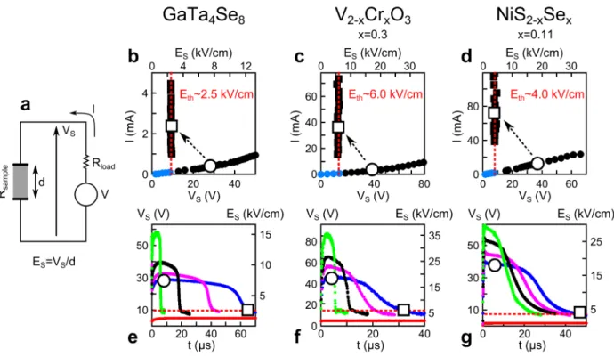
FIG. 1. a) The schematics of the experimental setup. b-g) Universal I − V characteristics (panels b, d, f) and time dependence of the sample voltage VS(t) (panels c, e, g) for three different types of narrow gap Mott insulators. Blue dots correspond to
the region below Eth, where no breakdown is observed. Black symbols correspond to the I − V characteristic in the resistive
switching region, above Eth. The black dots show the initial I −V , before the breakdown, and the black squares indicate the final
state. The open symbols highlight a particular breakdown transition for easier visualization. Measurements on GaTa4Se8were
performed at 77 K, on V2−xCrxO3 (x=0.3) at 164 K and on NiSe2−xSx (x=0.11) at 4 K. For further experimental details see
the Supporting Information.
tor to metal transition driven by pressure,24–29which is
in good qualitative agreement with the theoretical pre-dictions of Hubbard model studies in dynamical mean field theory.14,30 The first compound is actually a repre-sentative of a whole family of Mott systems, the AM4Q8,
with A=Ge, Ga, M=Ta, Nb, V, Mo and Q=Se, S.25
No-tice that an electric-field driven transition has also been reported in VO2. However, unlike the Mott insulators
in the present study does not have a pressure induced transition, but a first order insulator to metal transition driven by increasing temperature.23,31–34This is
qualita-tively different to the present case, since the resistivity of our systems merely shows thermal activated behavior with small gaps of the order of tenths of eV. In Figure 1 we present the I −V curves of the measured resistive tran-sitions of the three Mott systems. They all show similar behavior with a sharp transition onset at an electric field threshold Eth. The data also show the delay times for
the transition td. As mentioned before, the magnitudes of
these quantities are off by at least three orders of mag-nitude from estimates obtained from solutions of Hub-bard models.12,13,15,16We should also emphasize that the
sharp transition is indicative of its electronic origin. In fact, a reduction of resistance due to Joule self-heating would produce and S-shaped I − V characteristic with a
gradual evolution of the resistance change.35
The resistor network model is schematically shown in Figure 2, where each one of the cells represents a small region of the physical system, which is in either of two well defined electronic states, Mott insulator (MI) or cor-related metal (CM). Since the compounds are normally insulators, we assume that the MI-state is lower in en-ergy, which we define as the reference EMI≡ 0. The
CM-state is assumed to be a metastable CM-state, with a higher energy ECM, and separated from the MI by an energy
barrier EB (see Figure 2). These features are based on
previous studies of the Mott-Hubbard transition,14 that have successfully captured many (equilibrium) proper-ties of this transition.24,36 Indeed, the dynamical mean
field theory studies on the Hubbard model predict the existence of two competing states, very close in energy, which have a region of coexistence close to the first order Mott metal-insulator transition.14 In our model, the MI and CM states are associated with corresponding high and low resistance values, RMI and RCM. The cells are
assumed to represent patches of at least a few nanome-ters in size, such that an electronic state may be well defined. Initially all cells are assumed to be in the MI-state. The time is discretized and the external voltage is applied to the MRN at each timestep. The local voltage
3
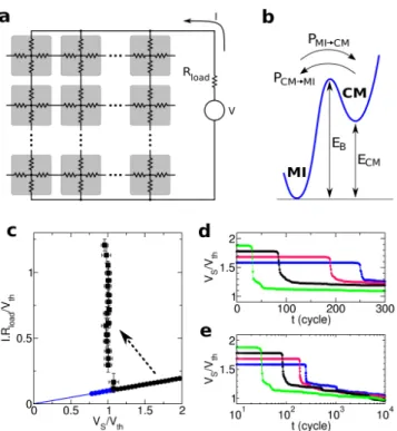
FIG. 2. a) Mott resistor network model and simulation cir-cuit, in analogy with the experimental setup. b) Energy di-agram of the CM and MI states and the energy barrier. c) Simulation data of the I-V characteristics, following the same convention as in Fig. 1. d) Time dependence of the sample voltage as a function of simulation time. The data correspond to VS/Vth= 1.74, 1.84, 1.95 and 2.06, from right to left. e)
Same as panel (d) on semi-log scale to observe the long time behavior.
drops ∆V (r) are then computed by standard methods.37 We assume that the MI → CM transition rate of each cell is given by PMI→CM = ν e−(EB−q∆V )/kT, where the
constant ν is an attempt rate, which we set to unity and similarly the charge q. The precise origin of this transition is not yet fully established. It may be likely driven by injected carrier doping, due to impact ionisa-tion, which could induce the local metalization of a small region.32,33 However, other mechanisms including
elec-tromechanical coupling cannot be ruled out,38 as Mott
insulators may have significant compressibility anoma-lies near the metal-insulator transition. After a MI → CM transition, the metastable CM-state may relax back to the MI by overcoming the energy barrier EB, with
a transition rate given by PCM→MI = ν e−(EB−ECM)/kT.
Notice that, since RMI RCM, the voltage drop may be
neglected in the CM cells. This relaxation process de-fines an important time scale in the problem, as we shall later see. Under these assumptions, the model can be solved by numerical simulations in discretized time (see Supporting Information for details). In analogy to the ex-perimental setup (see Figure 1), we apply a voltage to the network VS = [RS/(RS+ RL)]V , where V is the
exter-nal voltage, RS is the equivalent resistance of the network
and RLis a limiting load resistance. Initially, all the cells
are in the MI state, and RS = R0MI= g RMI, where g is a
geometrical factor of the order of unity. Then, during the simulation, the sites may switch between the MI and CM states, and thus the value of RS is recomputed at every
timestep. The specific values of the adopted parameters are detailed in the Supporting information.
As shown in Figure 2, the simulations predict a sharp threshold behavior for the MRT phenomenon and I − V characteristics that are in excellent agreement with the experimental data of Figure 1. Moreover, the simula-tions also capture the qualitative behavior of the time delay td, which increases dramatically as the voltage
ap-proaches the threshold from above, and eventually di-verges as Vs→ Vth.
While one may expect that the sharp threshold stems from a simple percolation process, in fact the simula-tions unveil a qualitatively different scenario. At low ap-plied V , after an initial transient, the fraction of sites in the CM to those in the MI state stabilizes and is simply given by the ratio between the transition rates PMI→CM/PCM→MI, which is small since (EB− ECM) <
(EB− ∆V ). Beneath the threshold, ∆V ≈ V /M , where
M is the number of cell layers between the electrodes (see Figure 2). This reflects the equilibrium of concentration condition NMIPMI→CM= NCMPCM→MI.
In a simple percolation picture, the 2D (site) perco-lation fraction ∼0.59 would be reached when the ap-plied voltage is such that ∆V ≈ ECM.39 However, in
our model, already for voltages well beneath that value the MRT takes place in a dynamically directed avalanche phenomenon. The reason may be simply understood. At low PMI→CM rates (i.e., low applied V ), the CM sites
are diluted and randomly distributed. However, as V is increased the production rate of CM sites grows, and eventually there is a significant chance of having a few consecutive CM sites longitudinally aligned, in a direc-tion perpendicular to the electrodes. The voltage drop in that low-RCMmetallic segment decreases, and induces
a compensating increase of the voltage drop at the high-RMI sites that are close to its extremes. Thus, the
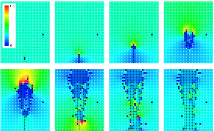
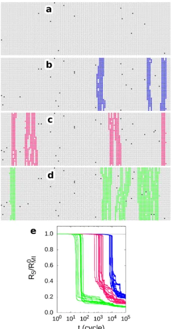
tran-sition probability MI → CM for those sites increase as well, which quickly get added to the metallic segment and further increase the voltage drop at the extremes, even-tually leading to a runaway process, or avalanche. This is the dynamically generated directed percolation lead-ing to the MRT. This is visualized in detail in Figure 3, which shows the formation of a conductive path and the enhanced transition probability that develops along the longitudinal direction. Interestingly, this picture is key to understanding many experimental features, and leads to further predictions that we shall test later. In Figure 4, we show the snapshots of the state of the system after a long period of a continuously applied V . Beneath the Vth
the production of CM sites remains very diluted and far from percolation, with no precursors. From the observa-tion of the panels corresponding to VS above and below
4
FIG. 3. Intensity color plot of local voltage drops on the resistor network ∆V /EB. Only the region where the filament forms
and the breakdown occurs is shown. The electrodes are at the top and bottom of the panels. The applied voltage is VS/Vth
= 1.74, the panes correspond to simulation time t = 60, 70, 75, 80, 83, 85, 87 and 100 (See Supporting Information for the animated data). The state of each cell is represented by a white or a black dot, for MI and CM, respectively.
of CM sites, which is much smaller than the 2D percola-tion value menpercola-tioned before. Above the threshold, quite surprisingly, we observe that the number of conductive paths (or the fraction of the system that is in transited state) increases with the voltage difference to the thresh-old, VS−Vth. We trace this effect to a rapid succession of
multiple avalanche events. In fact, after the initial path is formed, so long as the voltage on the sample remains above Vth, the avalanche events will continue until the
applied voltage on the sample decays down to the value Vth(see Figure 2e).
Another interesting prediction of the model is that the low resistance state is not permanent. Since the CM states are metastable, after the applied voltage is switched off, all those sites begin to relax back to the MI state. Thus, Mott resistive transition is, unlike, the permanent dielectric breakdown phenomenon in semicon-ductors, a volatile effect (i.e., the resistance recovers its original value after the applied voltage is switched off) with a characteristic relaxation time trelax Indeed,
ex-periments reported in the GaTa4Se8compound show this
sudden recovery effect.8–11 Therefore, the Mott resistive
transition phenomenon is a volatile and fully reversible resistive switching, which is qualitatively different to the nonvolatile resistive switching effect in transition metal oxide systems.7,40–42
We finally consider a non-trivial prediction, which
fol-lows from the assumptions of our model. Since, one of its key features is relaxation of the CM cells back to the MI state, we may expect a qualitative different behav-ior if we apply short voltage pulses (i.e., of a duration smaller that the respective td), which are repeated at a
time interval that may be either shorter or longer than trelax. In fact, since a single pulse is too short to produce
the transition, in the case of long time intervals between pulses the effect of each one vanishes due the relaxation before the next pulse arrives. In contrast, if the interval between pulses is shorter than trelax, then the effect of
successive pulses will accumulate, and eventually drive the transition. In Figure 5 we show the theoretical pre-diction along with the respective experimental data in the GaTa4Se8 Mott insulator. An excellent qualitative
agreement is observed, which provides a definite nontriv-ial validation of our model.
In conclusion, we found universal behavior in electric field-induced insulator-to-metal transition experiments of various prototypical narrow-gap Mott insulator com-pounds, V2−xCrxO3, NiS2−xSex and GaTa4Se8. These
features motivated the formulation of a resistor network model, which we studied numerically. We obtained excel-lent agreement with the experimental data, and also with a non-trivial delayed voltage pulsing experiment pre-dicted by the model. The numerical simulations showed that the physical origin of the Mott resistive transition is
5
FIG. 4. Local resistance snapshot of the network after a long simulation time of 105 cycles. The black and color dots
indi-cate the sites that are in the CM state, while the grey dots correspond to the sites in the MI state. The dots forming filaments are coloured for easier visualization. The initially applied sample voltage were VS/Vth = 0.7, 1.1, 1.4 and 1.8
(panels (a) to (d)). The right panel (e) shows the dependence of the normalized network resistance (RS/RMI0 ), as a function
of simulation time. The color notation is as in the previous panels. The dispersion of the data corresponds to 10 runs with different seeds, which illustrate the effect of the finite size of the network.
a dynamically directed avalanche mechanism. Our study brings new insight to the difficult problem of the behav-ior of Mott systems out of equilibrium, and is a timely stepping-stone for research in the emerging field of Mot-tronic devices.
FIG. 5. Electric pulsing with varying pulse-interval time. a) Sample voltage VSas a function of time of a GaTa4Se8-based
device upon the application of a train of voltage pulses of 60 V and duration of 20 µs with a period τ =100 µs. Notice that for a continuously applied voltage of 60 V, the device switches after a delay time of td= 70µs (see Supporting
In-formation). b) Simulation data for a train pulse showing the same qualitative behavior. c) Experimental number of pulses required for switching as a function of the pulse period. The pulse duration is as in (a). The grey area corresponds to a pulse-interval where switching no longer occurs. It indicates that the trelax∼ 800µs. d) Simulation results for varying the
pulse-interval. Error bars are due to finite size effects.
ACKNOWLEDGMENTS
This work was supported by the French Agence Na-tionale de la Recherche through the funding of the “NanoMott” (ANR-09-Blan-0154-01) and “Mott-RAM” (ANR-2011-EMMA-016-01) projects. The authors ac-knowledge Prof. Aharon Kapitulnik, Prof. D. Roditchev, Dr T. Cren and Dr V. Ta Phuoc for useful discussions.
1 I. H. Inoue and M. J. Rozenberg, Adv. Funct. Mater. 18,
2289 (2008).
2 H. Y. Hwang, Y. Iwasa, M. Kawasaki, B. Keimer, N.
Na-gaosa, and Y. Tokura, Nat Mater 11, 103 (2012).
3 “International technology roadmap for semiconductors,”
http://www.itrs.net/ (2011).
6
5
M. Nakano, K. Shibuya, D. Okuyama, T. Hatano, S. Ono, M. Kawasaki, Y. Iwasa, and Y. Tokura, Nature 487, 459 (2012).
6
S. Asanuma, P.-H. Xiang, H. Yamada, H. Sato, I. H. In-oue, H. Akoh, A. Sawa, K. Ueno, H. Shimotani, H. Yuan, M. Kawasaki, and Y. Iwasa, Appl. Phys. Lett. 97, 142110 (2010).
7
M. Rozenberg, Scholarpedia 6, 11414 (2011).
8 L. Cario, C. Vaju, B. Corraze, V. Guiot, and E. Janod,
Adv. Mater. 22, 5193 (2010).
9
E. Souchier, L. Cario, B. Corraze, P. Moreau, P. Mazoyer, C. Estourn`es, R. Retoux, E. Janod, and M.-P. Besland, Phys. Status Solidi RRL 5, 53 (2011).
10
J. Tranchant, E. Janod, L. Cario, B. Corraze, E. Souch-ier, J.-L. Leclercq, P. Cremillieu, P. Moreau, and M.-P. Besland, EMRS 2012 Symposium L, Thin Solid Films 533, 61 (2013).
11 C. Vaju, L. Cario, B. Corraze, E. Janod, V. Dubost,
T. Cren, D. Roditchev, D. Braithwaite, and O. Chauvet, Microelectron. Eng. 85, 2430 (2008).
12
T. Oka and H. Aoki, Phys. Rev. B 81, 033103 (2010).
13 F. Heidrich-Meisner, I. Gonz´alez, K. A. Al-Hassanieh,
A. E. Feiguin, M. J. Rozenberg, and E. Dagotto, Phys. Rev. B 82, 205110 (2010).
14 A. Georges, G. Kotliar, W. Krauth, and M. J. Rozenberg,
Rev. Mod. Phys. 68, 13 (1996).
15
T. Oka, R. Arita, and H. Aoki, Phys. Rev. Lett. 91, 066406 (2003).
16
T. Oka and H. Aoki, Phys. Rev. Lett. 95, 137601 (2005).
17
Y. Taguchi, T. Matsumoto, and Y. Tokura, Phys. Rev. B 62, 7015 (2000).
18 S. Dutta, S. Lakshmi, and S. K. Pati, J. Phys.: Condens.
Matter 19, 322201 (2007).
19
M. Eckstein, T. Oka, and P. Werner, Phys. Rev. Lett. 105, 146404 (2010).
20
C. H. Ahn, A. Bhattacharya, M. Di Ventra, J. N. Eck-stein, C. D. Frisbie, M. E. Gershenson, A. M. Goldman, I. H. Inoue, J. Mannhart, A. J. Millis, A. F. Morpurgo, D. Natelson, and J.-M. Triscone, Rev. Mod. Phys. 78, 1185 (2006).
21 C. Vaju, L. Cario, B. Corraze, E. Janod, V. Dubost,
T. Cren, D. Roditchev, D. Braithwaite, and O. Chauvet, Adv. Mater. 20, 2760 (2008).
22 F. Sabeth, T. Iimori, and N. Ohta, Journal of the
Ameri-can Chemical Society, J. Am. Chem. Soc. 134, 6984 (2012).
23
T. Driscoll, J. Quinn, M. Di Ventra, D. N. Basov, G. Seo, Y.-W. Lee, H.-T. Kim, and D. R. Smith, Phys. Rev. B 86, 094203 (2012).
24
M. Imada, A. Fujimori, and Y. Tokura, Rev. Mod. Phys. 70, 1039 (1998).
25 R. Pocha, D. Johrendt, B. Ni, and M. M. Abd-Elmeguid,
Journal of the American Chemical Society, J. Am. Chem. Soc. 127, 8732 (2005).
26 E. Dorolti, L. Cario, B. Corraze, E. Janod, C. Vaju, H.-J.
Koo, E. Kan, and M.-H. Whangbo, Journal of the Ameri-can Chemical Society, J. Am. Chem. Soc. 132, 5704 (2010).
27 V. Guiot, E. Janod, B. Corraze, and L. Cario, Chem.
Mater. 23, 2611 (2011).
28
S. Miyasaka, H. Takagi, Y. Sekine, H. Takahashi, N. Mˆori, and R. J. Cava, J. Phys. Soc. Jpn. 69, 3166 (2000).
29
V. Ta Phuoc, C. Vaju, B. Corraze, R. Sopracase, A. Peruc-chi, C. Marini, P. Postorino, M. Chligui, S. Lupi, E. Janod, and L. Cario, Phys. Rev. Lett. 110, 037401 (2013).
30 G. Kotliar and D. Vollhardt, Physics Today 57, 53 (2004). 31
H.-T. Kim, B.-J. Kim, S. Choi, B.-G. Chae, Y. W. Lee, T. Driscoll, M. M. Qazilbash, and D. N. Basov, J. Appl. Phys. 107, 023702 (2010).
32
H.-T. Kim, B.-G. Chae, D.-H. Youn, S.-L. Maeng, G. Kim, K.-Y. Kang, and Y.-S. Lim, New Journal of Physics 6, 52 (2004).
33
V. Guiot, L. Cario, E. Janod, B. Corraze, V. Ta Phuoc, M. Rozenberg, P. Stoliar, T. Cren, and D. Roditchev, Nat Commun 4, 1722 (2013).
34
A. Zimmers, L. Aigouy, M. Mortier, A. Sharoni, S. Wang, K. G. West, J. G. Ramirez, and I. K. Schuller, Phys. Rev. Lett. 110, 056601 (2013).
35 B. K. Ridley, Proceedings of the Physical Society 82, 954
(1963).
36
P. Limelette, A. Georges, D. J´erome, P. Wzietek, P. Met-calf, and J. M. Honig, Science 302, 89 (2003).
37
S. Kirkpatrick, Rev. Mod. Phys. 45, 574 (1973).
38
V. Dubost, T. Cren, C. Vaju, L. Cario, B. Corraze, E. Janod, F. Debontridder, and D. Roditchev, Adv. Funct. Mater. 19, 2800 (2009).
39
D. Stauffer and A. Aharony, Introduction To Percolation Theory (Taylor & Francis, 1992).
40
A. Sawa, Materials Today 11, 28 (2008).
41
R. Waser, R. Dittmann, G. Staikov, and K. Szot, Adv. Mater. 21, 2632 (2009).
42 Y. V. Pershin and M. Di Ventra, Advances in Physics,