5
UNIVERSITE DE SHERBRpOKE3 llSb OOblH 21E1 0
UNIVERSITE DE SHERBROOKE
Faculte des sciences appliquees
Departement de genie electrique et de genie informatique
rK
510l^
,^5'3
nw
7'^
REALISATION D'UN SYSTEME DE TRANSMISSION DE DONNfeES
A SPECTRE ETENDU
UTILISANT COMME CANAL UNE LIGNE D'ENERGIE ELECTRIQUE
(110V/60Hz)
M6moire de maitrise 6s sciences appliqu6es
Sp6cialit6 : g6nie 61ectrique
Uu Jiansheng
Sherbrooke (Quebec), CANADA
Juin 1994
1*1
of Canada Acquisitions andBibliographic Services Branch
395 Wellington Street
Ottawa, Ontario
K1A ON4
du Canada
Direction des acquisitions et des services bibliographiques
395, rue Wellington
Ottawa (Ontario) K1AON4
Your file Votre r616rence
Our tile Notre r616rence
THE AUTHOR HAS GRANTED AN
IRREVOCABLE NON-EXCLUSIVE
LICENCE ALLOWING THE NATIONAL
LIBRARY OF CANADA TO
REPRODUCE, LOAN, DISTRIBUTE OR
SELL COPIES OF fflS/HER THESIS BY
ANY MEANS AND IN ANY FORM OR
FORMAT, MAKING THIS THESIS
AVAILABLE TO INTERESTED
PERSONS.
L'AUTEUR A ACCORDE UNE LICENCE
IRREVOCABLE ET NON EXCLUSIVE
PERMETTANT A LA BIBLIOTHEQUE
NATIONALE DU CANADA DE
REPRODUIRE, PRETER, DISTRTOUER
OU VENDRE DES COPmS DE SA
THESE DE QUELQUE MANIERE ET
SOUS QUELQUE FORME QUE CE SOIT
POUR METTRE DES EXEMPLAIRES DE
CETTE THESE A LA DISPOSITION DES
PERSONNE INTERESSEES.
THE AUTHOR RETAINS OWNERSHIP
OF THE COPYRIGHT IN fflS/HER
THESIS. NEITHER THE THESIS NOR
SUBSTANTIAL EXTRACTS FROM IT
MAY BE PRINTED OR OTHERWISE
REPRODUCED WITHOUT fflS/HER
PERMISSION.
L'AUTEUR CONSERVE LA PROPRIETE
DU DROIT D'AUTEUR QUI PROTEGE
SA THESE. N1 LA THESE N1 DES
EXTRAITS SUBSTANTffiLS DE
CELLE-CI NE DOIVENT ETRE D^IPRIMES OU
AUTREMENT REPRODUITS SANS SON
AUTORISATION.
ISBN 0-612-04570-6
To
My wife
Jianhua
and Hy daughter
SOMMAIRE
Ce memoire presente un systeme de transmission de donnees utlllsant comme
canal une Ugne d'energie electrlque (en anglals. Power Line CaTTierfPLC)). Ce systeme est realise a 1'aide de la technique de spectre etendu.
Le chapitre 1 resume en bref quelques applications possibles de systemes PLC, leurs partlcularites et classtflcation de meme que quelques considerations speciales au
systeme PLC propose ainsi qu'un cahler de charge sommaire du systeme a concevotr.
Le chapltre 2 presente les caracteristiques de la Ugne d'energie electrique, a savoir: son brult et son Interference, 1'attenuation, I'lmpedance et les particularites de transmission. Le chapltre 3 presente quant a lui la technique de communication a spectre etendu et son application dans un systeme PLC.
Le chapitre 4 decrit la configuration du systeme PLC propose, Ie format et la forme d'onde du signal, ainsl que la structure des donnees. Un modele de simulation et les resultats de Panalyse spectrale bases sur ce modele sent egalement Ulustres dans ce
chapitre.
La conception des circuits et des logiciels du systeme PLC est detalllee respectlvement aux chapitres 5 et 6.
Le chapltre 7 presente la configuration du montage utilise pour les tests et les resultats obtenus des mesures effectuees sur ce systeme. La conclusion et des suggestions cTameUoratlon du systeme sont aussi presentees dans ce chapltre.
Les schemas detallles du systeme, 1'organigramme du loglciel et la liste de tous les
A ckn o wledsme n t
ACKNOWLEDGMENT
The author gratefully acknowledges Prof. Noel Boutin for his guidance during the past two years. It would have been impossible for me to complete this research project without his help, in both academic and financial respects.
The all PCBs and cabinets of the system were designed and constructed by Mr.
Pierre A. Savard. The author appreciates his contribution to this research project.
The author want also to express his appreciation to Mr. Richard Letoumeau for
his help in the aspect of supplying the devices, the elements and the measurement instruments demanded by this project.
The author is Indebted to all peoples who have contributed their time and ingenuity to this work.
TABLE OF CONTENTS
1 iisrmoDucnoN... i 2 POWERUNEPROPEKnES... 2 2.1 Noise... 5 2.2 Attenuation... 8 2.3 hnpedance... 9 2.4 Transmission Characteristics... 113 SPREAD SPECTRUM TECHNIQUE & PLC SYSTEM... 13
3.1 Basic Anti-Interierence Principle ofSS System... 13
3.2 Spread Spectrum Code Sequence... 15
3.2.1 Spectmm Feature... 16
3.2.2 Autocorrelatlon Feature... 17
3.3 Comb Notch Filter ~ Special Consideration for PLC Applications. ... 18
4 SYSTEM DESCRIPTION... 25
4.1 Basic System Configuration... 26
4.2 Signal Format and Waveform... 28
4.2.1 About CEBus... 28
4.2.2 Data Packet Stmcture... 33
4.2.3 Waveform and Spectrum... 36
4.3 System Architecture... 41
4.4 Transmitting Path Description... 43
4.4.1 Spread Specti-um Operation... 43
4.4.2 Carrier Modulation... 44
4.5 Receiving Path Description... 48
4.5.1 Choice for Clock Recovery Approach... 49
4.5.2 Correlator and Synchronization Mechanism... 50
5 SYSTEM IMPLEMENTATION — HARDWARE DESIGN... 54
5.1 Programmable Logic Device (PLD)... 55
5.2 The Central Control Unit... 57
5.3 The Filter Unit... 59
5.3.1 The Input and Post Band-Pass Filter... 59
5.3.2 The 60Hz Notch FUter... 61
Table of Contents 5.4 Frequency Reference... 68 5.4.1 PLL Circuit... 68 5.4.2 Shaping Circuit... 74 5.4.3 Dividing Circuit... 74 5.5 Correlator... 76 5.5.1 Hardlimiter... 76
5.5.2 Interpretation of Correlation Process... 77
5.5.3 Correlation in Non-error Situation... 79
5.5.4 Correlation on The Received Signal with error... 81
5.5.5 Detection Threshold Value... 81
5.5.6 Analysis of Miss and False Alarm Error Rates of The Con-elator... 82
5.5.7 Implementation of The Correlator... 84
5.6 Synchronization Circuit... 85
5.6.1 Clock Synchronization... 86
5.6.2 Frame Synchronization... 91
5.6.3 Analysis of Miss and False Frame Synchronization Error Rates. ... 96
5.7 Power Amplifier and Coupling Network... 97
5.7.1 Power Amplifier... 97
5.7.2 Coupling Network and TX/RX Switch... 99
6 SYSTEM IMPLEMENTATION — SOFTWARE DESIGN... 101
6.1 Brief Introduction to MC68HC11... 101
6.2 General Description of The Software... 104
6.3 Jitter-Smoothed 60Hz Reference Subsystem... 108
6.4 The Ttansmitting Flow... 109
6.4.1 Data/Address Registers in The Transmitting Flow... Ill 6.4.2 Control/Flag Registers in The Transmitting Flow... 113
6.4.3 Explanation of The Transmitting Flow... 114
6.5 The Receiving Flow... 116
6.5.1 Data/Address Registers in The Receiving Flow... 116
6.5.2 Control/Flag Registers In The Receiving Flow... 118
6.5.3 Explanation of The Receiving Flow... 121
6.5.4 Discussion about The Data Decision... 124
7 MEASUREMENT AND CONCLUSION... 126
7.1 Data Source... 126
7.1.1 Scrambler and Descrambler... 126
University of Sherbrooke
7.1.2 The Relationship between The Bit Errors and The Output of The
Descrambler....;... 128
7.2 Test Configuration... 128
7.3 Signal to Noise Ratio... 129
7.4 Results and Conclusion... 131
ANNEX A: SCHEMATIC OF UNTTS... 136
A-l. The central control unit (UNIT 1)... 137
A-2. The filter unit (UNIT 2)... 138
A-3. The frequency reference generator/ correlator unit (UNTT 3)... 139
A-4. The power supply and PA unit (UNTT4)... 140
ANNEX B: PROGRAM FLOW CHARTS... 141
B-l. PSDATA... 142 B-2. INTPAI... 143 B-3. GTBYTE... 144 B-4. SNSRV... 145 B-5. D^TIC2... 146 B-6. INTOC2... 148 B-7. INTOC3... 149
ANNEX C: PROGRAM UST... 150
List of Figures and Tables
LIST OF FIGURES AND TABLES
Figure 2.1 Examples of specific noise spectra present on low voltage
distribution wires... 7
a) Voltage spectrum for synchronous noise (light dimmer) around 12480Hz b) Voltage spectrum for noise created by universal motor (smooth spectrum) c) Voltage spectrum for non synchronous periodic noise (from television receiver) Figure 2.2 typical residential background noise spectrum on 240V circuit... 8
Figure 2.3 Variation in Attenuation for a 100-foot long power line on different days and frequencies... 9
Figure 2.4 Power line characteristic impedance... 10
Figure 2.5 Transmission characteristic of power line... 12
a) Typical transmission vs. frequency characteristic of power line b) Channel characteristic of a power line channel loaded with some specific devices Figure 3.1 Anti-interference principle by the SS technique... 14
Figure 3.2 Power spectrum of a PN sequence... 16
Figure 3.3 Power spectrum distribution for a modulated PN sequence. ... 17
Figure 3.4 Auto-correlation function waveform of a M-sequence... 18
Figure 3.5 System configuration of proposed system... 19
Figure 3.6 Frequency response characteristic of the comb filter... 21
Figure 3.7 Automatic frequency tracking notch filter... 22
Figure 3.8 Precoder and comb notch filter... 23
Figure 3.9 Filtering process for packeted data... 24
Figure 4.1 Block diagram of the proposed system... 26
Figure 4.2 Frame format of CEBus... 29
Table 4.1 CEBus symbol encoding... 30
Figure 4.3 Symbol encoding in CEBus... 31
Figure 4.4 Spread specti^im carrier chirp in CEBus... 31
Figure 4.5 Preamble waveform of ASK: "1101"... 32
Figure 4.6 Packet body waveform of PRK: "1101"... 32
Figure 4.7 Proposed data format... 34
a) Data packet structure b) Packet after passing through the comb filter Figure 4.8 Synchronization byte structure... 35
Figure 4.9 Control byte stincture... 35
Figure 4.10 PN sequence base-bandwavefonn... 36
Figure 4.11 Simulation model for spectrum analysis... 37
Figure 4.12 Transmltterwaveform... 38
Figure 4.13 Simulation model for spread spectrum operation... 39
Figure 4.14 Simulation model for modulation operation... 40
Figure 4.15 Power spectral density for signal in the transmitter... 40-41 Figure 4.16 System composition block diagram... 42
Figure 4.17 Normal spread specb-um operation... 43
Figure 4.18 Spread spectrum generation by switching between two PN sequences... 44
Figure 4.19 Circuit of the transmitting path... 45
Figure 4.20 BPSK operation by modulo-2 adder and D-trigger... 45
Figure 4.21 Waveforms and timing relationship in the transmitter... 47
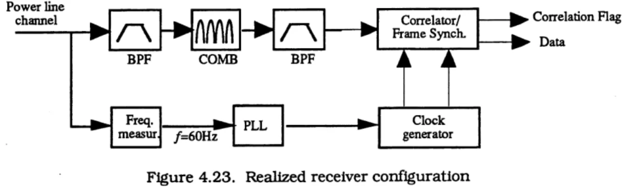
Figure 4.22 Basic receiver configuration... 48
Figure 4.23 Realized receiver configuration... 49
Figure 4.24 Basic principle of a serial correlator... 51
Figure 4.25 Functional block diagram of a serial correlator... 51
Figure 4.26 Basic principle of a parallel con-elator... 52
Figure 5.1 Basic macrocell architecture of the 5C060... 55
Figure 5.2 5C060 global architecture... 56
Figure 5.3 Configuration of the central control unit... 58
Figure 5.4 Basic connection of the MAX275... 60
Figure 5.5 Frequency response characteristic of the input band-pass fUter and the post band-pass filter... 61
Figure 5.6 Configuration of the digital 60Hz notch filter using a digital subtractor... 62
Figure 5.7 Configuration of the digital 60Hz notch filter using an analog subta"actor... 63
Figure 5.8 Configuration of digital time-delaying circuit... 65
Figure 5.9 Timing relationship tn the 60Hz notch filter... 65
Figure 5.10 Frequency response characteristic of the 60Hz notch filter... 67
Figure 5.11 Frequency reference system... 68
List of Figures and Tables
Figure 5.12 Pins assignation ofXR-215... 70
Figure 5.13 Typical circuit connection for frequency generation... 70
Figure 5.14 Internal configuration of the loop divlder... 73
Figure 5.15 Waveform shaping... 75
a) Waveform limlter and shaping circuit b) Wavefonn of shaping circuit Figure 5.16 Schematic of the hardlimiter... 76
Figure 5.17 Input-output voltage hysteresis characteristic of the Schmitt-Trigger... 77
Figure 5.18 Model for con-elator operation on signal centered at o)c... 78
Figure 5.19 InterpretationofBPSKmodulated symbols... 78
Figure 5.20 Basic structure of the correlator... 80
Figure 5.21 Logic organization of the correlator... 85
Figure 5.22 Clock and frame synchronization systems... 86
Figure 5.23 Waveform features, timing information and sampling instants of the signal x(Q... 87
Figure 5.24 Sampling tnstant for the ideal and degraded signals... 88
Figure 5.25 Configuration of the CSS system... 89
Figure 5.26 Pulse-edge detector circuit... 89
Figure 5.27 Multlple-phase generator... 90
Figure 5.28 Excess pulse locked ctrcuit... 91
Figure 5.29 Waveform of the CSS system... 91
Figure 5.30 Output of the correlator... 92
Figure 5.31 State transitions of FSS... 93
Figure 5.32 Frame synchronization system... 95
a) Frame synchronization system configuration b) Signals and states transitions in the FSS Figure 5.33 The power amplifier and the hlgh-pass filter... 98
Figure 5.34 Coupling network and TX/RX switch... 99
Figure 6.1 Block diagram of MC68HC11... 102
Figure 6.2 MC68HC11 programmer's model... 103
Figure 6.3 Defaultmemoiy map for the normal expended mode... 104
Figure 6.4 Actualmemoiy map of the system... 105
Figure 6.5 I/O pin applications of the MC68HC11A1... 106
Figure 6.6 Global system program flow... 107
Figure 6.7 Operation sequence of the JSR subsystem... 108
Figure 6.8 Programming model for the transmitting flow... 110
Figure 6.9 Transmitting flow... 115
Figure 6.10 Programming model for the receiving flow... 117
Figure 6.11 Receiving flow... 120
Figure 6.12 Packet synchronization process... 122
Figure 6.13 Different results in the RXRGS in the situation of some pulses missing from the CL sequence... 123
Figure 6.14 Output data bits and clock... 124
Figure 7.1 Scrambler and descrambler... 127
Figure 7.2 Testing circuit... 129
Figure 7.3 Narrow pulse noise signal... 129
Figure 7.4 The received BPSK signal waveform... 130
Figure 7.5 Bit error rate perfonnance of the PLC system... 131
Figure 7.6 Miss packet synchronization rate of the PLC system... 132
Table 7.1 Measurement results on power line... 133
Chavter 1 — Introduction
CHAPTER 1
INTRODUCTION
Using power lines as a transmission media is not a quite new idea. As early as
1950's, some international organizations published several standard documents related to power Une carrier (PLC) applications [1]. In the beginning, the request was for a simple
and a low rate message transmission tn analog mode between an energy supplier and
thetr consumers. Today with the development of computer local area networks (LAN's) and the various of electric/electronic utilities and sendces, a cheap and readily available transmission media is a must. The Power line seems to be a good candidate for this requirement considering its presence in already completed installation and its ease of accessibility. The progress in the digital data communication field also makes a practical data transmission system based on the power line channel possible. The potential application areas of such a data transmission system may include [2-5]:
• Intrabuilding LAN for computer applications; • Building environmental management;
• Home electrical utilities monitoring and control; • Security and fire alarm monitoring;
• Electronic messaging;
• Others
However, as a transmission media, the properties of the power Une are not good
enough to support communication requirements because it was not originally designed for this purpose. Usually, the power line suffers from high and unpredictable variations
in impedance, signal attenuation, interference and noise. Overcoming those
last years, considerable effort has been devoted to realize practical communication
systems on such a channel. Many research results have shown that spread spectrum
communication technique is a good candidate for this application.
The spread spectrum(SS) communication technique was developed primarily for military and secure purpose. However, as time goes on, it was found that the SS technique
can be used in many more applications due to its excellent properties of anti-interference, multiple-access and low power spectral density. Since interference and noise in the power line occupy a quite wide frequency range with a relatively high density, a narrow-band system, has almost no chance to perform in their presence. On the other hand, the SS technique presents some advantages In this situation. Many PLC systems based on
the SS technique have been studied, and each one leads to different system configurations
and performances [2, 6, 7, 8].
Almost all researchers in this area believe that reducing the affection of noise and interference is the most important topic to consider when designing a PLC system. In past studies, the proposed interference rejection methods mainly fall into two categories. One kind of methods works with the help of a noise notch filter. It uses a notch filter designed with nuUs at 60 Hz (the AC power source frequency) and its harmonic frequency. It has a relatively simple configuration but suffers from a low data rate limit (according to the published results, the actual data rate could reach only one half of the power source frequency—30bits/sec.)[9]. Furthermore, this type of systems is also sensitive to the frequency shtft of the power source because it is normally designed for a fixed frequency situation. It therefore cannot be thought as a practical system. Another type of methods uses adaptive filter algorithms to match the variable status of the power line [10], but its complexity and computation cost limit its application area.
To realize a practical system with an ideal noise and interference cancellation
Chavter 1 — Introduction
the proposed system, the SS technique is retained in order to keep a low spectral density
and a good Immunity to the narrow-band interference. A multiple notch receiver filter
synchronized with the frequency of the power source is used to reject Its affection. Since the parameters of the filter would track the frequency drift of the power source system, it is not frequency sensitive and Is able to keep the suppression capability of the 60Hz and its harmonies. More important, the data rate provided by this system can reach a quite high level, and therefore could match to the normal data rate of standard data interfaces
(for example: 2400 bits/sec. 4800 bits/sec,... 19.200 bits/sec). This shows a possibility
of using the system in an intrabuUding environment for a real application purpose.
Based on this idea, a practical data transmission system was buUt up. Its basic
specifications are given as follows:
• Center frequency: 134.4KHz
• Spread spectrum bandwidth: 268.8KHz • Channel Modulation: DS-SS-BPSK
• Channel transmission rate: 9.6kbits/sec. • Data rate: 4.8kbits/sec.
• Signal formation: Packet
This system is a variant of a Direct-Sequence Spread-Spectrum (DS-SS) system. In the input stage of the receiver, a specially designed comb notch filter Is inserted to
attenuate the 60Hz power source components and Its harmonies to a level as low as
possible. It effectively protects the data receiving circuits from such Interferences. Data are transmitted on the channel in a packet format. This establishes a good basis for a further high level error control strategy (for instance: ARQ). In the design of the clock/frame synchronization circuit, the correlator and the comb notch filter, programmable logic devices (PLD) are used so that powerful and easily modtfiable functions are obtained within a compact size. The whole system is constructed around a
microprocessor and thus requires a relatively simple hardware structure. With the
powerful processing capability of the microprocessor, many signal processings such as the reference generating, the spread spectrum modulating, the data buffering and
decision, etc., are done by software instead of hardware. It makes the system having a
flexible configuration. The experimental results have shown that the system possesses a
pretty good interference and noise suppression performance. With some Improvements
and modifications, it could provide relatively reliable data transmission capability on the power line with comparable low hardware cost. All the details of the system will be
Chapter 2 — Power Line Properties
CHAPTER 2
POWER LINE PROPERTIES
The power lines could be divided tnto two types: high voltage transmission trunks and low voltage distribution wires (110/220V). As a communication media, the first is usually used for remote control and telemetry systems, and the latter is suitable for the
Information transmission over a relatively short distance and thus is our major study object.
It is well known that a communication channel is usually corrupted by a certain
amount of noise and/or interferences. In regular channels (wire or wireless), Gaussian noise is the main source of noise. With the power line, however, the situation is quite
different. The 60Hz component of power source system and its harmonies are the biggest
noise sources for a PLC system. The interferences from other equipments plugged on the power line are also very strong as compared with the Gaussian noise. DtEFerences between
a power line channel and a regular transmission media could also be found with respect
to other parameters, such as line loss, impedance, frequency characteristics, ... etc.
Thus, a good understanding of the properties of a power line is a necessary element in the research of a good PLC system.
2.1 Noise
Noise on low voltage distribution wires (also called residential power line) can generally be classified into four groups as follows [11, 12]:
a) Noise sunctvonous with the 60Hz power sustem freauencu
This noise is caused by switching devices, such as silicon-controlled rectlflers (SCR's) and certain power suppliers. This noise is synchronous with, and drifts with, the
60Hz power frequency. As Its name Implies, this noise has spectral lines at multiples of
60Hz (Figure 2.1-a).
b) Noise with a smooth spectrum.
This noise is often caused by loads on the line that do not operate synchronously with the power line frequency, such as universal motors used In many household appliances and workshop electric tools. This noise can be thought of as having a smooth spectrum without stationary spectral lines. Over a small bandwidth, this noise may be
modeled as white noise (Figure 2.1-b).
c) Slnale-Event impulse noise
Lightning, thermostats, and switching of electrical utilities or devices, such as
capacitor banks, create the impulse noise.
d) Non sunchronous periodic noise
This noise has line spectra uncorrelated with the 60Hz power frequency. The most common source of this type of noise is television receivers generating noise at multiple of the 15.734KHz horizontal line scanning frequency (Figure 2.1-c).
Besides those mentioned above, background noise, typically Gaussian, also exist on the power line.
Figure 2.2 gives a typical residential background noise spectrum on 240V-circuit. The result contains the near flat spectrum of Gaussian noise, television video signal and
60Hz and its harmonies components. As one can easily see, the 60Hz and its harmonies noise have level 10-30dB above the flat noise spectrum.
Chapter 2 — Power Line Proverties
-I—I-208(A &*moaic
«"r«a cavelojx of 60, Rz odd •nvcl.op*
11968 12224 12*«) 12736 Frequency la kflz "Sw -20 J. -60 J.
-I—I—I—^
-I—^ AO 60-I—I—h
FrequcncT la kHz(a)
(b)
^—I—I—I—I—I—I—I—(--w J.M--LUJ|
-I—^ *o to Frcquenor la kSr 80 100(0
Figure 2.1 Examples of specific noise spectra present on low voltage distribution wires 111]
a) Voltage spectrum for synchronous noise (light dimmer) around
12480Hz
b) Voltage spectrum for noise created by universal motor (smooth spectrum)
c) Voltage spectrum for non synchronous periodic noise (television receiver)
0 —20 > 0-w *rf • h S-60. 1 "-<».
^—I—I—I—•-—I—I—(—I—I—t
^ 4- -t—h 20 *0 60 Freqweacy In kHzFigure 2.2 Typical residential background noise spectrum on 240V circuit [11]
2J2 Attenuation
It is veiy dif&cult to obtain an accurate attenuation characteristic of a power Hne. The obseryation results reported In some papers 13, 6] show that it not only varies with location sites, but also with time because every changing load on the power line, such as when electrical equipment Is plugged In or unplugged, switched on or off, will results in change of attenuation characteristic.
The attenuation of a power Bne consists of the line attenuatlon (due to resistance, radiation. Induction, etc.), the shunt attenuatlon (power flowing into paths other than the desired channel), the bypass losses (some equipment has a capacitor at the primary side of their AC power transformer), and the coupling losses. Furthermore, if no perfect match exists between power line and coupling device tmpedance, mismatch losses wffl
also be present.
Figure 2.3 gives a typical attenuatlon characteristic for a 100-foot long power-ltae path. It could be seen that the attenuation curve tends to be flat in a relatively narrow bandwidth but varies greatly with time. The attenuation of the power line tends to
Owpter 2 — Power Line Properties
Increase as the frequency increases. The difference between the attenuatlon values at different frequencies and time may be as high as to 50-70 dB.
-100
Figure 2.3 Variation tn attenuation for a 100-foot long power line on different days and frequencies [6].
2.3 Impedance
The characteristic impedance of a transmission line is defined as the ratio between the voltage and current of a traveling wave on a line of Infinite length. In some studies, fhe power line Is treated as a transmission line (8, 13, 14]. Tlius the characteristic impedance of the power line may be estimated by
^R+jcoL
">~\'G^jwC
However, this equation does not gtve an accurate enough Impedance value for the power
line due to too many branchings and loads of various impedances.
In practical applications, a value of impedance to which the carrier coupling equipment is matched in order to obtain minimum mismatch and maximum power transfer Is often used to represent characteristic impedance of the power line. Many researchers have published real observation results at different sites and times. There Is
large difference among those observation results. However, a common conclusion can be
obtained from those measurements: the characteristic impedance of the power line is a function of frequency. It has a very low value at the lower frequency range (below 100KHz) and Increase as the frequency increases. Figure 2.4 shows a real measurement result of the power line characteristic impedance by using the line impedance stabilization network (USN) technique (14].
I
20kHz »MHz
Figure 2.4 Power line characteristic Impedance (14J
Chavter 2 — Power Line Proverties
From the results, it can be concluded that the power line can be considered as a low
impedance transmission line. In the frequency range below 500KHz, its typical
impedance value Is around 1-50 ohms. Since most of the electrical equipments connected
to the power line have a parallel capacitor at their AC input terminals, the power line characteristic impedance wiU obviously appear as capacitive.
2.4 Transmission characteristics
Using a power line as a transmission media is no more unregulated. Many
countries have adopted regulations. Concerning the allocated frequency band, a range from 30KHz to 300KHz is assigned for PLC systems in the United States. In Canada, limited use is made of frequency from 10 to 490KHz. There are also some countries that use frequencies as high as 500KHz [1].
The frequency characteristic that the power line presents within its assigned frequency band is a very important issue to a PLC system. Unfortunately, as other
characteristics mentioned above, the transmission characteristic of the power line changes greatly with different sites and times. Figure 2.5-a gives a rough measurement result of the transmission vs. frequency characteristic of a power line. Figure 2.5-b shows
the same channel characteristic obtained when different loads are plugged on the line [5].
All studies mentioned that the power line possesses many attractive features due
to its convenience and low cost. On the other hand, however, it Is a very hostile transmission environment compared with other regular wires or wireless channels. It is almost Impossible to realize a reliable data transmission on it unless some special techniques are used.
S^zat Iramnmu <aB) -20 + -30+ 40 ^ •50+ 0«tper ( (kH;) 50 100 ISO 200
(a) Typical transmission vs. frequency characteristic of power line
S<yal Transrni*s«3<i << -20 -30 -40 •50 !)
a) without special loading
b) with a minico<nput<
/
/'
c) wrtti a capacrtory
nputer^
» (kHz) 50 100 150 200(b) Channel characteristic of a power line channel k>aded with
some specSc devices
Figure 2.5 Transmission characteristic of power line
Chaster 3—Syread Spectrum Techniaue Qf PLC System
CHAPTER 3
SPREAD SPECTRUM TECHNIQUE & PLC SYSTEM
The spread spectrum (SS) technique has decades of history by now. Its development origin can even be traced back to 20s—30s of this century [16]. Its Initial military purpose made it having great progress during and after World War II. Its applications could be found In Radar, navigation, electronic counter measures (ECM) and
electronic counter-counter measures (ECCM), communications... etc. In
communication area, the SS technique presents a superior anti-interference performance over other communication techniques. Combtned with present digital
communication technologies, the SS communication system is playing an increasingly Important role today.
3.1 Basic Anti-Interference Principle of SS System
The core content of the SS technique is a coherent transformation in the frequency domain. The two basic processing operations, spreading and despreading frequency spectra, are based on the use of an identical synchronized spread spectrum code
sequence at both transmitter and receiver. The sequence is a periodic binary bit stream
that has a pseudo-random distribution property of Its bit-Is and bit-Os. This property makes the sequence look like wide band noise.
A brief indicative block diagram of the process is given in Figure 3.1. At the transmitter, the original data (KD with rate of Rd bits/sec modulates the spreading code sequence of rate J?ss bits/sec , which is far higher than that of d(t). This is so-called the
spreading process. At the receiver, an operation called despreading is taken place by
using a same sequence as the one used at the transmitter in conjunction with a device called as correlator . When a match is reached between the received signal and the local
code sequence, the correlator has a maximum value of output. The original message d(t) is recovered and resumes its original bandwidth. On the other hand, the energy of noise and interference added during the transmission process is spreaded over the bandwidth of the
sequence, and thus produces little efiTect on the recovered narrow-band signal.
Noise
B^~
TRANSMITTER Spread^tv 1
RECEIVER Data Data Noisew
PN sequenceFigure 3.1 Antl-interference principle of the SS technique
A basic performance measure of a SS system is the processing gain defined as:
(3.1)
G=-^
where:
^
RSS — spreading code sequence rate tn bits per second
Rd — data rate in bits per second
It represents, to a certain degree, how much anti-interference capability a SS system
could obtain compared with regular narrow-band systems through the spreading
—despreading process.
According to the way the spreading code sequence Is used, SS systems can be classified tn the following four types of modes [17]:
• Direct Sequence Spreading (DS)
Chapter 3 — Spread Spectrum Technique 6' PLC System
• Frequency-Hopping (FH) • Timlng-Hopping (TH)
• Linear Frequency Modulation (Chlrp)
In PLC applications, DS system seems to be a good choice due to Its simplicity. Depending on the data modulation mode, it could be further divided into PAM, FM,
DS-BPSK, DS-QPSK,... and so on. DS-BPSK is known as the most popular mode, and will
be the one retained in the present study.
3.2 Spread Spectrum Code Sequence
The correlation operation tn the receiver of the DS system is based on the
assumption that the spreading sequence used in the system has pure noise properties, i.e., the sequence is aperiodic and has completely random distribution of "lws and U0"s. In
practice however, it is impossible to establish synchronization between the transmitter
and receiver by using such a sequence. Instead of a pure noise sequence, the most
popularly used spreading sequence for the SS system is a periodic sequence called
pseudo-random or pseudo-noise sequence, or PN sequence in short. Maximum-length linear shtft-register sequence , called M-sequence , is a typical one among several candidates.
This M-sequence can be easily generated by a shift register of length N . It has the following features [17]:
• The periodic property
The M-sequence wiU repeat itself in a period of p bits given by
p=22v-l (3.2)
where: N is the length of the shift register used for generating the sequence .
Due to this property, the M-sequence cannot be known as a "pure random" one.
• The balance property
In each complete period of the sequence, the number of bit ulws differs from the
number of bit "0"s by at most 1.
• The run property
In one complete period of the sequence, there are 2 ^ ^ runs (consecutive "lns or "CTs) with length I, a run of N u lws and a run of (N -1) "0"s.
• The correlation property
If an exact period of the sequence Is compared, bit by bit, with any shtft of Itself, the number of agreements differs from the number of disagreements by at most 1.
3.2.1 Spectrum Feature
A blpolar NRZ formatted version of a PN sequence has a power spectrum distribution as shown in Figure 3.2. It could be found that there are discrete spectrum
lines at frequencies equal to 2rrw/p (m=l,2,3....), in which p represents the repeat period of the PN sequence. It's power spectrum envelop has nulls at ko)c (fc= 1,2,3....), <a>c being the
clock driving frequency of the shift register for generating the sequence.
sr
uQ
0
^
SS -10
u>-»&
coI
PLi -2027C/P
Ih-\.
2jc/p
COrJOc
coFigure 3.2 Power spectrum of a bipolar version of PN sequence
Chapter 3 — Spread Spectrum Technique 6' PLC System
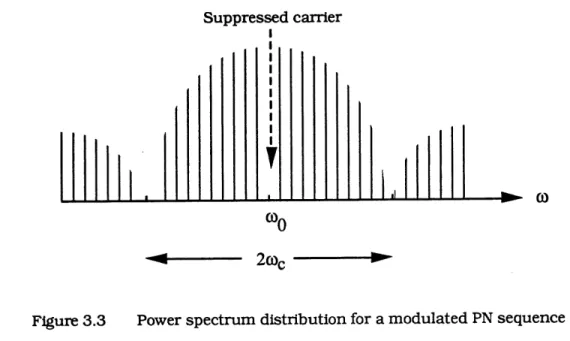
If the bipolar PN sequence is modulated on a high frequency carrier OQQ,, Its power spectrum Illustrated in Figure 3.2 will be shifted to the carrier frequency (OQ, as shown in
Figure 3.3 (assuming a carrier-suppress modulation mode used).
Suppressed carrier
co
co,'0
20)r
Figure 3.3 Power spectrum distribution for a modulated PN sequence
Obviously, if a narrow-band data signal is modulated on a PN sequence which is
then further modulated on a carrier for transmission, the final power spectrum of the signal transmitted on the channel will correspond to the narrow-band spectrum of the data signal translated around each separated spectral line appearing in Figure 3.3. Therefore, the whole frequency bandwidth of the transmitted signal, after the spreading operation, will be proportional to the driving clock frequency of the sequence generator.
3.2.2 Autocorrelation Feature
The auto-correlation function of a continuous signal^ is usually defined as
RW=\W^f(t-i}dt
(3.3)For a discrete sequence x(i) with length {, its auto-con-elation function may be written as
(-1
-^
n=0
R(k)=^x(i)x(i-kT)
(3.4)234567
I I
-1
^
Figure 3.4. Auto-correlation function waveform of a M-sequence
A M-sequence of amplitude +1 or -1 whose repeat period is p has an correlation function waveform as illustrated in Figure 3.4. It may be found that the auto-correlation function R(k) reaches its maximum value only when the relative shift is zero,
pf
i.e., RW =2" -1 when k =0, p, 2p, .... Elsewhere fhe auto-correlation function keeps a very low value. This sharp auto-correlation characteristic is the key feature which permits
signal identification and synchronization.
3.3 Comb Notch Filter — Special Consideration for PLC Applications
The SS technique can advantageously be used for PLC systems mainly because of
its superior anti-tnterference performance. However. in an extremely bad transmission
environment like power line, it is still very difficult to obtain a satisfactory result by simply using the SS technique. Some special actions must be considered to overcome the effects of the non ideal transmission characteristics of the channel. A variety of actions and system considerations were suggested and tried by many researchers in this area.
Those systems showed up different configurations and performance. Some time ago, Prf.
Noel Boutin had proposed a DS-PLC system structure that merges together the advantages and beneficial features of some existing systems (15]. Among other things, a special action was considered for eliminating the afiFection from the 60Hz power system signal
Chapter 3 — Spread Spectrum Technique £r PLC System and It's harmonies.
In a power distribution network, the 110V/60Hz (or 220V/ 50Hz In some countries) signal component is the most important actor. When the power line is also used as a data transmission media, that signal becomes one of the biggest source of interference due to:
• Its high amplitude
There are very few of other noise/interference sources having an amplltude comparable with the 60Hz component.
• Itsconstancy
It occupies the media all the time unless the power supply is switched o£f.
• Its harmonies
Because of the imperfections of the electricity generating and transforming equipment and the effects of many electrical utilities connected to the line, the 60Hz
signal is usually not a perfect sine wave. A lot ofharmonic components are also present.
Hence, eliminating the effect of the 60Hz signal component and its harmonies is a basic but important requirement to any PLC system.
DEC -DATA
OUT
TRANSMTTTER RECEIVER
CHANNEL
Figure 3.5 System configuration of proposed system
A special attention is paid to this problem In the proposed system shown in block diagram in Figure 3.5. The core part of the system is a comb filter shown In the shaded block. This filter has nulls at frequencies of 60Hz and its harmonies. By putting this comb filter at the input stage of receiver, most of the energy of the 60Hz signal and its harmonies coming from the power line channel is expected to be eliminated. The later data detecting circuits could therefore operate in a relatively clean environment.
The comb filter Is a first-order system having the following transfer function:
H(Jfi))=l- e-JO)Td (3.5)
Its corresponding normalized amplitude vs. frequency response and phase vs. frequency response could thus be expressed as
IH(co)l= l-cosfi)Td (3.6)
e=tan-^ma^ (3.7)
i-cosfur^
It is easy to see that there are multiple zeros for I H(co) I at frequencies
Q)Td=2rw n?=0,1.2,3,
i.e., f= n/Td (3.8)
where: Td is the delay time provided by the delay device of the filter. Should the delay
time be properly selected to be equal to the period of power source waveform, i.e,: 1/60
second, the filter will have transmission zeros right at 60Hz and its hannonics as shown
in Figure 3.6. Due to its frequency response feature, this filter is called a comb notch
filter.
^
100
Chapter 3 — Spread Spectrum Technique 6" PLC System
200 300
Frequence, Hz
400
500
Figure 3.6 Frequency response characteristics of the comb filter
Clearly, the null frequencies precision of the filter is determined by the delay time Td provided by the delay device. A computer simulation showed that a BPSK system may keep its reliable transmission ability provided that the delay time error is less than 1,40th of the carrier period (15]. It is not a difficult task to design a filter with such a
delay time precision for a fixed Td. Unfortunately, in the real power line network, many
factors make the power system frequency drift from its specified value — 60Hz. Worse, this drift is irregular and thus cannot be described by any presently available algorithm. Hence, it is impossible to design a fixed-parameter comb filter that could keep a stable notching performance for such a frequency variable signal.
One solution to this problem is setting up an automatic frequency tracking system which will keep optimum performances of the filter in the whole frequency drifting range. SpectflcaUy. one must always keep the delay time of delay device to be equal to
Td=^/FpL (3.9)
where FPL, is the power system frequency, whose nominal value is 60Hz. Therefore a
practical comb filter for eliminating the 60Hz signal and its harmonies should have a
structure like the one shown in Figure 3.7. In this system, the power source frequency is monitored to generate a reference. A tracking system works on this reference to guarantee
that Td satisfies equation (3.9).
Data in
60Hz~
Fre.samp.
Filter out
Figure 3.7 Automatic frequency tracking notch filter
By using such a comb notch filter, it is expected that the affection from the 60Hz
power source signal and its harmonies may be greatly reduced. At the same time,
however, the desired signal stream coming from the channel wiU be also afifected by the notching characteristic of the filter. Since the output of the filter is a linear composition of the signal itself coming from the channel and its delayed counterpart, it will be a distorted version of the original signal sent by the transmitter. This is an undesirable result. In order to regenerate the original signal wavefonn from the output of the filter.
two measures may be considered:
(a) Insert a precoder at the transmitter. This precoder must have a transfer function of the form
1
H(z)=
1-z-1 (3.10)
The block diagrams of both the precoder and the notch filter are given in Figure 3.8 for comparison. The presence of the precoder cancels the effect of the notch filter on the received signal stream. From the viewpoint of the whole system, they therefore do nothing to the data signal transmitted through the system.
Chapter 3 — Spread Spectrum Technique <&' PLC System
IN
Td
-^OUT IN
-^<D-^OUT
PRECODER NOTCH FILTER
Figure 3.8 Precoder and comb notch fUter
The major drawback of the precoder is that It delivers a multi-level signal at its output. One solution would be to replace the algebraic adder by a module-2 adder. By doing so, the complexity of the whole system will increase because the data decision rule at the receiver wiU be the same as the one associated with a duobinary system [18,19].
(b) Restrain the length of the input data stream to a value equal to or less than the delay time Td. In other words, the data bits are sent from the transmitter in a packet mode instead of continuous mode by leaving enough time internal (equal to or larger than Td) between two packets . At the output of the notch filter, the time interval between two packets will be filled up by the delayed counterpart of the earlier packet. No overlap happens between two adjacent packets as long as the interval is chosen properly. This
process is illustrated in Figure 3.9.
Compared with method (a), method (b) has the follows advantages:
• There is no demand for extra circuits like the precoder at the transmitter. The system configuration thus becomes simpler.
• Signal stream at output of the filter may be detected and processed as binary data. This is usually easier than the duobinaiy data processing which has to work with a three level signal requiring adaptive thresholds.
• Packeted data can be easily formatted to include an error control strategy.
^
xd ^AdTd
m^
Td 2T^ 3T^
\
T<i 2T,, 3T^ 4T;
Figure 3.9 Filtering process for packeted data
Considering those facts, method (b) was retained as the solution which will be further studied in more detail In the next chapters.
Chapter 4 — System Description
CHAPTER 4
SYSTEM DESCRIPTION
The idea of a spread spectrum power line carrier communication system with harmonfc noise rejecffon capabiltty was brought forward by Prf. Noel Boutln In 1991 [15]. Since that time, a large amount of configuration studies and computer simulations were carried out in order to find a practical and realizable system. According to the specific application considered for the system, the matn technical specifications of the
system, e.g., the central frequency, the channel modulation mode and rate, the selection of PN sequence, etc., were determined. The actual design works began from September of
1992. A real system for performance test and verification purpose has been completed by the beginning of 1994.
The main application environments of this system will be normal offices, education buildings or residential houses. Therefore, high reliability and low cost should be the basic goals one should try to achieve. Although some newly developed products could be used for Implementing the system, they were not retained for reasons of cost and complexity. Instead, a microprocessor system(MC68HC 11) was used as the central control unit. Due to the powerful processing capability of the microprocessor, the system has a relative compact size and a greatly simplified hardware. Furthermore, since many
signal processing operations such as synchronization, correlation, and data decision are
fulfilled by programmable logic devices or software system, the system has a Hexible structure. It may be easily modified and updated for new requirements tn the future.
4.1. Basic System Configuration
The proposed system may be represented by the block diagram illustrated in
Figure 4.1. TRANSMITTER
d(t)
iBufferAl^
Buffer BLi
Spread s(t) BPSK MOD.Y ^
^lU'^Tl-fiLTp^
Conv. CouplerPN c(t) A
d(t)
DataDec. A,p(t)
Despread RECEIVER BPSK Demo. A z'(t) Comb Notcher BPF Power Line z(t)r ^
PN c(t)Figure 4.1 Block diagram of the proposed system
In the transmitter, the incoming data d(t) at rate Rd blts/sec. is first pushed
alternatively into two buffers, A or B. Since the system must work in a packet-data mode
in order to leave a large enough time internal between two data groups transmitted tn the channel, the transmitting rate Rf of the data tn the channel must be higher than the Incoming data rate Rd' If the ttme Interval between two packets equals the length of the packet, the transmitting rate in the channel should be equal to two times the rate of the Incoming data to ensure that all the incoming data bits could be sent out without
accumulation in transmitting side. In other words, the transmitter must have a
temporary register to save much enough incoming data bits to permit a packet transmission at double speed. The buffers A and B play this role in the transmitter. For easy management, it is desirable to fix the capacities of the buffers equal to the quantity of bits contained tn one packet. Doing so, the system can conveniently get out a packet
Chapter 4 — System Description
data stream by regularly switching the input and output paths of the buffers A and B. According to the requirement of the system. Rd is equal to 4.8kbits/sec., therefore R( , the transmission rate for the packet data, is selected to be 9.6kblts/sec.
The packet data is modulated on a PN sequence for the spreading spectrum operation. The baseband spread spectrum signal is then translated in frequency by a carrier c(t) In order to get a waveform suitable for transmission on the power line channel. The selection of the frequency of c(D should foUow two principles:
1) It should be high enough to permit a large spectrum spreading factor:
2) It should be such that most of the frequency components of the spread spectrum signal fall tn a range within which the power line has a relative
enjoyable transmission characteristic.
Considering that the power line shows high attenuatlon and impedance at higher frequencies and that there exist regulations restraining the operating frequency range of PLC applications (below 500KHz), the frequency of c(t) was chosen to be 134.4KHz (14
times the 9.6kbits/sec. channel transmission rate).
To obtain an efficient transmission and better anti-noise performances, the
unlpolar signal m(t) (zero and plus) is converted to a bipolar one x(t) (minus, zero and plus). That three-level signal is then amplified to the desired power level by the final power amplifier and Injected into the channel through a coupling network.
In the receiver, the signal coming from the power line is first passed through a fourth-order Butterworth band-pass filter to remove the noise and interference located outside the main spectrum lobe of the signal. The low cutoff frequency of the band-pass filter is set at 2KHz in order to provide a certain degree of suppression of the 60Hz power source signal and its low-order harmonies. The following comb notch filter will further
suppress the 60Hz and its harmonic components to a level low enough to obtain an
acceptable signal-to-noise ratio. Then, an inverse procedure of the one used at the
A
transmitter will be used to get d(f), an estimate of the original data d(D.
Compared with the transmitter, the receiver presents more challenges. Besides the classic problems met in normal narrow-band systems (such as clock and bit synchronization), some new topics particular to spread spectrum systems must be considered (correlation and sequence synchronization). Although there is a large amount of research results published about those topics, the final decision on which synchronization and detection systems to consider must be based on an analysis of the desired features of the whole system.
4.2 Signal Format and Waveform
Packet data transmission has been widely used in computer communication networks and other related communication areas. A variety of transmission protocols
have been published for different application environments. Some of them could be of
Interest for our packet data format.
4.2.1 About CEBus [20-26]
CEBusfConsumer Electronic Bus) is a communication protocol under active development by the Electronic Industries Association. Its application object is mainly for home communication, through which all the electronic appliances in a home will be able to communicate one with each other. Its supported media include optical fiber,
coaxial cable, twisted pair, RF and infrared transmission and power line. Its summary specifications are given below.
4.2.1.1 CEBus packet
A basic CEBus data packet consists of eight fields, as shown in Figure 4.2.
Chavter 4 — System Descrivtion
PRE
•<-CON
DA
DHC | SA | SHC
MAX. length = 344 bitsINFO
PCS
-^
Figure 4.2 Frame format of CEBus
where:
PRE - Preamble field
Random 8-blt non-information bearing field. Fixed length.
CON - Control field
Variable length with a maximum of 8 bits. Defines fhe frame type and the channel access priority.
DA - Destination Address field
Variable length with a maximum of 16 bits. Defines the receiving
node address.
DHC - Destination House Address field
Variable length with a maximum of 16 bits. Defines the address of the receiving home system that shares a common medium with the transmitting
node.
SA - Source Address field
Variable length with a maximum of 16 bits. Defines the transmitting
node address.
SHC - Source House Address field
Variable length with a maximum of 16 bits. Defines the address of the
transmitting home system.
INFO - Information field
Consists of an integer number of bytes up to a maximum of 32 bytes. Contains the Network Layer Protocol Data Unit ( NPDU).
FCS - Frame Check Sequence field
8-bit checksum of variable length.
The total number of bits per frame is 344 at maximum. For briefness, the sum of CON, DA, DHC, SA, SHC and INFO is called the "packet body".
4.2.1.2 Basic symbols and timing in CEBus
CEBus uses four symbols represented by Non Return to Zero(NRZ) Pulse Width
Encoding. These symbols are: 1. 0, EOF, and EOP and are encoded as shown in Table 4.1,
where 1 and 0 are two information bearing symbols, EOF is the end of field Indicator, and EOP marks the end of a packet. UST means one unit symbol time. With these symbols, a data packet in CEBus has the following structure:
[PRE] EOF [CON] EOF [DA] EOF [DHC] EOF [SA] EOF [SHC] EOF [INFO]
EOF FCS] EOP
Symbol « 1 »> "0"EOF
EOP
PreambleUST
1
2
8
N/A
Duration 114^5228ps
SOOps
N/A
Packet Body and FCS
UST
1
2
J_4
Duration lOOps200ps
300ps
400ps
Table 4.1 CEBus symbol encoding
The transmission medium is defined as having two basic states: SUPERIOR and INFERIOR. They are not assigned to any particular symbol. Any symbol can occur in
Chapter 4 — System Description
either the SUPERIOR or the INFERIOR state. It is the time between the state transitions that determines the symbol encoding. An example of CEBus symbol encoding is shown in
Figure 4.3.
SUPERIOR
J-l
i_m
1111
INRERIOR
1 0
EOF 1 0
EOP
Figure 4.3 Symbol encoding in CEBus
Assuming that the numbers of "1" and "0" in the contents of all fields are equal, the average encoding time for the whole data fields could be obtained by multiplying the number of data bits by a factor 1.5. Adding all the seven EOF symbols and one EOP symbol that has three and four unit's time respectively, the maximum possible length of a packet is
8<L5«114ms + (336-1.5 + 7*3 + l»4)«100ms = 54.268 ms
4.2.1.3 Modulation and waveform in CEBus
CEBus employs a series of short, self-synchronized, frequency swept "chirp" as the signaling waveform. The chirp is swept from approximately 200KHz to 400KHz and then from 100KHz to 200KHz In a duration of lOOps as the one shown in Figure 4.4.
^— lOOps —^
Figure 4.4 Spread spectrum carrier chirp In CEBus
Two different modulation modes are used for the preamble and the packet body respectively in CEBus. Amplitude Shift Keying (ASK) is used in the preamble of the
packet. ASK uses alternating SUPERIOR and INFERIOR states. A superior state is represented by the presence of a chirp, an inferior state by the absence of a chirp. An example of ASK is lllustracted in Figure 4.5.
T
Figure 4.5 Preamble waveform of ASK: "1101'
<()! I <(>2 | <{)1 (|>1 | <)>2
Figure 4.6 Packet body waveform of PPK: 1101
The data body of the packet uses another type of modulation mode—Phase Reversal Keying (PRK). It utilizes two phases of the superior state, SUPERIOR fi and SUPERIOR ,2, which are 180° out of phase with one another, to modulate the encoded
data. Figure 4.6 gives an example of PRK for data "1101".
Although the CEBus protocol has a robust performance in power line media, we cannot directly use it in our system. Due to the presence of the comb notch filter, it is clear that the length of the data packet tn our system cannot be longer than Td=l/60Hz,
i.e., approximately 16.7ms, to prevent the waveform overlap at the output of the filter.
Compared with it, CEBus uses a variable length packet which can have a duration as long as 54.268ms. Obviously, such a packet cannot pass through the comb notch filter without
waveform overlap. University of Sherbroolce
Chapter 4 — System Description
However, It is possible to incorporate some features of the data packet in CEBus into our data structure. For instance, setting a preamble In front of our data packet will help to improve synchronization and data detecting ability in an hostile transmission
environment. A new data packet structure could be considered.
4.2.2 Data Packet Structure
As previously specified, the data rate of the signal coming from the transmitting buffers is 9.6kbits/sec, and the length of one packet cannot be longer than Td=l/60Hz= 16.7ms. This means that the maximum quantity of bits In a packet is
N = TA- = , 1/6°, = 160(^f5) (4.1)
T^ 1/9600
or 20 bytes (160/8).
To Improve the synchronization performance of the data packet, we Insert a preamble, a synchronization character and a packet information character in front of the data body. The proposed packet structure is shown in Figure 4.7. Each data packet consists of 19 bytes(152 bits): one all-zero preamble byte. one synchronization byte, one control byte and sixteen data bytes. A time slot of one byte Is left after each packet. No data will be transmitted during that time. It is used to prevent possible collisions occurring between the original packet and its delayed counterpart due to an inaccurate delay time of the comb notch filter. Another function of the protection slot Is to ensure resynchronizatlon at the beginning of each packet. The affections of the error bits happening during the synchronization and data detection may be limited in the range of one packet by the slot.
The composition and the functions of each part of the packet may be respectively described as:
PRE — Preamble byte
This is an all-zero byte. Its consecutive eight UOWs provide the convenience for
Initial bit synchronization In the receiver. Meanwhile, it warns the receiver that a data packet is coming so that the receiver could get ready to monitor the signal from the
channel untU a non-zero symbol, i.e., the beginning of the PSYN character, is found.
Because of the Inverting function of the comb notch filter, the preamble byte will become an all-one one after passing through the filter. It could be used by the receiver for the Identification of the delayed packets.
l/60sec l/60sec
DATA
h
l/60secDATA
Protection slot(a) Data packet structure
l/60sec
w
DATA
Protection slot
(b) Packet after passing through the comb filter Figure 4.7 Proposed data format
PSYN — Synchronization byte
The synchronization byte consists of a "0" bit and a M-sequence of seven bits. It makes use of the sharp auto-correlation characteristic of the M-sequence to mark the University of Sherbrooke
Chapter 4 — System Description
start of the effective data within the packet. It would decrease the false-wamlng rate and
set a more robust synchronization mechanism. Its structure is given in Figure 4.8.
MSB LSB
0
1
0
1
0
0
1
1
Figure 4.8 Synchronization byte structure
CON — Control byte
This byte consists of two parts as shown in Figure 4.9.
MSB
STATE
LSB
INDEX
where
Figure. 4.9 Control byte structure
STATE : Indicate the efficiency of the data packet. It has two states:
0000 — means the packet is empty, l.e., the content of the packet serves
to no useful purpose.
1111 — means the packet is full, i.e., the content of the packet is effective and has a meaningful purpose.
DiDEX: Indicate the Index of the packet. Its value ranges from 0000 to
1111.
To keep a constant packet stream in the channel during the transmitting period, an empty packet has to be inserted when the external data terminal do not have enough data to pack an Integral packet. The receiver thus must be able to identify the content
efficiency of each received packet. The bits STATE provides the receiver this capability.
During the receiving period, the receiver must process two type of data packets: the original one coming directly from the channel and the delayed one coming from the comb notch filter. A unique identification of each packet will be helpful for the data detection and the decision processing. That is the mission of the bits INDEX. Although only stirteen Identifications can be provided by this section, it is much enough since the receiver needs to identify only the difference between two adjacent packets.
DATA — Data section
The DATA section of the packet is composed of sixteen bytes. It is the data body of
each packet.
4.2.3 Waveform and Spectrum
In the proposed system (Figure 4.1), d(t) , the data outcoming from the data terminal, is a NRZ base-band signal at rate of 4.8kbits/sec. It is packed Into packets of 152 bits in the buffer A or B. The output signal pW of the buffers Is chosen to be a bipolar-RZ signal at rate of 9.6kbits/sec. It should pass through the operations of spread spectrum, BPSK modulation and then is injected into the power line.
Figure 4.10 PN sequence base-band wavefomi
A 7-bit M-sequence, 1010011, is chosen as the PN sequence for the spread spectrum operation tn the system. Its base-band waveform signature Is given in Figure 4.10. To
match with the RZ code format of pW, its duration is chosen equal to half of each pWs pulse, i.e., the active pulse width of the RZ wavefomi. In this way, each RZ pulse of p(t) could be modulated by an integral PN sequence. Clearly, the frequency of the clock
driving the PN sequence generator should be:
fc= 7»2»9600 = 134.4KHz
Chaptej^4 — System Description
(4.2)
That is just fhe frequency of the carrier c(f) so that they may be derived from the same
frequency reference source.
Noise an interference
p(t)
TRANSMITTER
Spread spectrum BPSK s(t) ^/Os x(t)PN
c(t)
RECEIVER
i z(t)=x(t)+i(t)CHANNEL
Figure 4.11 Simulation model for spectrum analysis
In order to obtain the power spectral density (PSD) of the signals present at each stage of the system, a computer system simulation was done with the help of MATLAB on the basis of a system model shown tn Figure 4.11. The signal wavefonns used in the transmitter of this model are given in Figure 4.12. The PSDs of those signals were calculated by ustng 4096 points FFT. All the normalized PSDs obtained apprear in Figure
4.15.
In this simulation, a RZ pulse sequence at rate of 9.6kbits/sec was used for the data signal p(t) . This sequence was broken into sections of 152bits to simulate the data packet. Symbols "1" and symbols "0" in this sequence followed the random distribution
mle. Its PSD has nulls at the frequencies^ n • 19.2KHz , n=l,2.3... (see Figure 4.15-a).
The periodic PN sequence was obtained in the simulation by repeating the 7-bit M-sequence (1010011). Since the clock frequency of the PN sequence generator is
134.4KHz, the repeating frequency of the PN sequence is
fpn = 134.4KHz/7= 19.2KHz (4.3)
It can be verified by the sequence's PSD obtained by the simulation. Figure 4.15-b illustrates that the PSD of the PN sequence Is composed of a set of discrete spectral lines in intervals of 19.2KHz. As being expected, the intensity of those spectral lines decreases at a very slow rate. Its spectrum thus occupies a considerable frequency range and has nulls at the driving frequency (134.4KHz) and its harmonies.
1 bit duration (l/9.6kb/s)
University of Sherbrooke
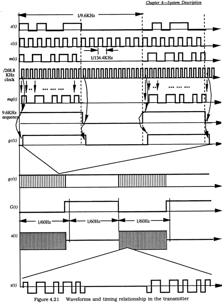
Chapter 4 —System Description
The base-band spread spectrum signal s(t) shown in Figure 4.12 can be seen as a
result of two operations on the PN sequence:
• Amplitude modulation: retaining the PN sequence In the first half of each bit duration of the data pW and suppressing the PN in the last half of the bit duration;
• Polarity modulation: In accordance with the polarity of the data p(t), changing the polarity of the retained PN according to the following rule:
f+7W(ioioon) p(t)=+i
[-7W(0101100) p(t)=-l
The simulation for the spread spectrum operation may be represented by the Indicative
diagram shown in Figure 4. 13. By this processing, the spectrum of the narrow-band data
signal p(t) is spread over the frequency bandwidth occupied by the PN sequence. From the PSD of the signal s(t) illustrated in Figure 4.15-c, it may be found that the first null
appears at 134.4KHz.
IF<tV(9» »- ^
+PN -PN
Figure 4.13 Simulation model for spread spectrum operation
Similarlly, the modulation operation tn this system can be modelized as a composition of two operations on the carrier c(t): being added to the signal s(t) and then multiplied by the the absolute value of the signal pW. This model is shown in Figure 4.14.
The PSD of the signal x(t) illustrated in Figure 4.15-d represents the spectrum of the signal injected into the power line. It shows that the spectrum of the signal
transmitted is continuous if the input data is a random sequence. This fact wlU greatly affect the design of the synchronization circuit of the system as it will be further
discussed in section 4.5.
p(t)
1-1
s(t)
-*\Q]
x(t)
c(t)
Figure 4.14 Simulation model for modulation operation
19.2KHz
0
19.2KHz
1 1.5 2
Frequency, Hz
(a) Envelop of PSD for p(t)
Spectrum Envelop 2.53
Xl05
101
e
"oQ
c^ Ox 10-7 10-15 0.51 1.5 2
Frequency, Hz 2.53
xl05
(b) Envelop of PSD for PN sequence
Figure 4.15 Power spectral density for signals in the transmitter
Chapter 4 — S-vstem Description
0
^
CL,102
10-11(H
10-7 lO-io0
0.5 134.4KHz1
1.5 2
Frequency, Hz (c) Envelop of PSD for s(t) Carrier 268.8KHz 2.53
xl05
Q
^
&110-3 I
10-4 l 1.5 2 Frequency, Hz (d) Envelop of PSD for xWFigure 4.15 Power spectral density for signals in the transmitter (continued)
4.3 System Architecture
The PLC system is built up around a central controlling unit (CCU) composed of a microprocessor—MC68HC 11 and related peripheral devices. Almost all of the processings of the base-band signal is performed with the microprocessor. The system works in a slmple-duplex mode. The mode switch between transmitting and receiving may be controlled manually or automatically by software.
The whole system block diagram is shown In Figure 4. 16.
The transmitting path accepts the base-band spread spectrum signal at the rate of 134.4kblts/sec from the CCU. Then it converts the signal to the required format and send It out, through an electronic T/R switch controlled by the CCU, on the power line. In the receiving mode, the signal from the power line channel Is fed through the T/R switch tnto the receiving path. The CCU starts data processing when It receives a synchronization identification signal from the receiving path. The data stream at rate of 9.6kbits/sec coming from the correlator circuit in the receiving path is sampled by the CCU and further processed by software. The CCU provides an asynchronous data output at rate of 4.8kbit/sec which can be accepted by an external data terminal. A standard RS-232 data interface could be easily realized by adding some simple circuits.
Data in
4.8kb/sec
Data out' Power
line
(baseband-134.4kb)
Sync.ident
for freq. measure & average
Figure 4.16 System composition block diagram
An external PLL system supplies the clock signals at different rates required by both the transmitting and the receiving path. The clock generator is synchronized on a jitter-smoothed frequency reference provided by the CCU. The reference has the same frequency as the AC power supply system but rejects its instantaneous fluctuations. It set up a basis means of establishing synchronization between the transmitting and receiving nodes through the power distribution network by using the 60Hz power source signal.
![Figure 2.1 Examples of specific noise spectra present on low voltage distribution wires 111]](https://thumb-eu.123doks.com/thumbv2/123doknet/5005726.124836/19.918.85.817.129.829/figure-examples-specific-noise-spectra-present-voltage-distribution.webp)

![Figure 2.3 Variation tn attenuation for a 100-foot long power line on different days and frequencies [6].](https://thumb-eu.123doks.com/thumbv2/123doknet/5005726.124836/21.918.195.764.167.605/figure-variation-attenuation-foot-long-power-different-frequencies.webp)