HAL Id: hal-00952121
https://hal.archives-ouvertes.fr/hal-00952121
Submitted on 26 Feb 2014
HAL is a multi-disciplinary open access
archive for the deposit and dissemination of
sci-entific research documents, whether they are
pub-lished or not. The documents may come from
L’archive ouverte pluridisciplinaire HAL, est
destinée au dépôt et à la diffusion de documents
scientifiques de niveau recherche, publiés ou non,
émanant des établissements d’enseignement et de
Phase regeneration of DPSK signals in a silicon
waveguide with reverse-biased p-i-n junction
Francesco da Ros, Dragana Vukovic, Andrzej Gajda, Kjeld Dalgaard, Lars
Zimmermann, Bernd Tillack, Michael Galili, Klaus Petermann, Christophe
Peucheret
To cite this version:
Francesco da Ros, Dragana Vukovic, Andrzej Gajda, Kjeld Dalgaard, Lars Zimmermann, et al.. Phase
regeneration of DPSK signals in a silicon waveguide with reverse-biased p-i-n junction. Optics Express,
Optical Society of America - OSA Publishing, 2014, 22 (5), pp.5029-5036. �10.1364/OE.22.005029�.
�hal-00952121�
Phase regeneration of DPSK signals in a
silicon waveguide with reverse-biased
p-i-n junction
Francesco Da Ros,1,*Dragana Vukovic,1Andrzej Gajda,2,3 Kjeld Dalgaard,1Lars Zimmermann,3Bernd Tillack,2,3
Michael Galili,1Klaus Petermann,2and Christophe Peucheret1,4
1Department of Photonics Engineering, Technical University of Denmark, 2800 Kgs. Lyngby,
Denmark
2Institut f¨ur Hochfrequenz- und Halbleiter-Systemtechnologien, TU Berlin, Einsteinufer 25,
10587 Berlin, Germany
3IHP, Im Technologiepark 25, 15236 Frankfurt (Oder), Germany
4FOTON Laboratory, CNRS UMR 6082, ENSSAT, University of Rennes 1, 22305 Lannion,
France
*fdro@fotonik.dtu.dk
Abstract: Phase regeneration of differential phase-shift keying (DPSK) signals is demonstrated using a silicon waveguide as nonlinear medium for the first time. A p-i-n junction across the waveguide enables decreasing the nonlinear losses introduced by free-carrier absorption (FCA), thus allowing phase-sensitive extinction ratios as high as 20 dB to be reached under continuous-wave (CW) pumping operation. Furthermore the regeneration properties are investigated under dynamic operation for a 10-Gb/s DPSK signal degraded by phase noise, showing receiver sensitivity improvements above 14 dB. Different phase noise frequencies and amplitudes are exam-ined, resulting in an improvement of the performance of the regenerated signal in all the considered cases.
© 2014 Optical Society of America
OCIS codes: (060.5060) Phase modulation; (070.4340) Nonlinear optical signal processing;
(190.4380) Nonlinear optics, four-wave mixing.
References and links
1. R. Slav´ık, F. Parmigiani, J. Kakande, C. Lundstr¨om, M. Sj¨odin, P. A. Andrekson, R. Weerasuriya, S. Sygletos, A. D. Ellis, L. Gr¨uner-Nielsen, D. Jakobsen, S. Herstrøm, R. Phelan, J. O’Gorman, A. Bogris, D. Syvridis, S. Das-gupta, P. Petropoulos, and D. J. Richardson, “All-optical phase and amplitude regenerator for next-generation telecommunications systems,” Nat. Photonics 4, 690–695 (2010).
2. Z. Tong, C. Lundstr¨om, P. A. Andrekson, C. J. McKinstrie, M. Karlsson, D. J. Blessing, E. Tipsuwannakul, B. J. Puttnam, H. Toda, and L. Gr¨uner-Nielsen, “Towards ultrasensitive optical links enabled by low-noise phase-sensitive amplifiers,” Nat. Photonics 5, 430–436 (2011).
3. K. J. Lee, F. Parmigiani, S. Liu, J. Kakande, P. Petropoulos, K. Gallo, and D. J. Richardson, “Phase sensitive amplification based on quadratic cascading in a periodically poled lithium niobate waveguide,” Opt. Express 17, 20393–20400 (2011).
4. B. J. Puttnam, D. Mazroa, S. Shinada, and N. Wada, “Large phase sensitive gain in periodically poled lithium-niobate with high pump power,” IEEE Photon. Technol. Lett. 23, 426–428 (2011).
5. T. Umeki, M. Asobe, and H. Takenouchi, “In-line phase sensitive amplifier based on PPLN waveguides,” Opt. Express 21, 12077–12084 (2013).
6. R. Neo, J. Schr¨oder, Y. Paquot, D-Y. Choi, S. Madden, B. Luther-Davies, and B. J. Eggleton, “Phase-sensitive amplification of light in aχ(3)photonic chip using a dispersion engineered chalcogenide ridge waveguide,” Opt. Express 21, 7926–7933 (2013).
7. N. Kang, A. Fadil, M. Pu, H. Ji, H. Hu, E. Palushani, D. Vukovic, J. Seoane, H. Ou, K. Rottwitt, and C. Peucheret, “Experimental demonstration of phase sensitive parametric processes in a nano-engineered silicon waveguide,” in Conference on Lasers and Electro-Optics, CLEO (2013), paper CM4D.7.
8. Y. Zhang, C. Husko, J. Schr¨oder, S. Lefrancois, I. Rey, T. Krauss, and B. J. Eggleton, “Record 11 dB phase sensitive amplification in sub-millimeter silicon waveguides,” in Conference on Lasers and ElectroOptics Pacific
Rim, CLEO-PR (2013), postdeadline paper PD1b-3.
9. Y. Zhang, C. Husko, J. Schr¨oder, S. Lefrancois, I. H. Rey, T. F. Krauss, and B. J. Eggleton, “Phase-sensitive amplification in silicon photonic crystal waveguides,” Opt. Lett. 39, 363–366 (2014).
10. A. C. Turner-Foster, M. A. Foster, J. S. Levy, C. B. Poitras, R. Salem, A. L. Gaeta, and M. Lipson, “Ultrashort free-carrier lifetime in low-loss silicon nanowaveguides,” Opt. Express 18, 3582–3591 (2010).
11. A. Gajda, L. Zimmermann, M. Jazayerifar, G. Winzer, H. Tian, R. Elschner, T. Richter, C. Schubert, B. Tillack, and K. Petermann, “Highly efficient CW parametric conversion at 1550 nm in SOI waveguides by reverse biased p-i-n junction,” Opt. Express 20, 13100–13107 (2012).
12. F. Da Ros, D. Vukovic, A. Gajda, L. Zimmermann, K. Petermann, and C. Peucheret, “Continuous wave phase-sensitive four-wave mixing in silicon waveguides with reverse-biased p-i-n junctions,” in European Conference
on Optical Communication (2013), paper P.2.11
13. W. Sfar Zaoui, A. Kunze, W. Vogel, M. Berroth, J. Butschke, F. Letzkus, and J. Burghartz, “Bridging the gap between optical fibers and silicon photonic integrated circuits,” Opt. Express 22, 1277–1286 (2014).
1. Introduction
In recent years, a renewed interest in all-optical phase-sensitive processing has lead to several breakthroughs being reported, spanning from differential phase-shift keying (DPSK) regener-ation [1] to low noise amplificregener-ation [2]. The nonlinear medium of choice for these results has been highly nonlinear optical fibers (HNLFs). However, in order to obtain the large nonlinear phase shifts required for practical applications, long interaction lengths are needed due to the relatively low nonlinear coefficients of silica HNLFs. Furthermore, one of the major practical difficulties with the implementation of phase-sensitive functionalities in silica HNLFs is the mitigation of stimulated Brillouin scattering (SBS). A widely used SBS suppression technique is phase dithering of the pumps, which may disturb the phase coherence between the interacting waves and may therefore not be compatible with the realization of phase-sensitive functionali-ties.
Alternative nonlinear materials may offer more compact implementations as well as better SBS immunity. Phase-sensitive amplification has been successfully shown by exploiting second order nonlinearities in periodically-poled lithium niobate (PPLN) waveguides [3–5]. Recently, the first demonstration of phase-sensitive amplification exploiting third order nonlinearities in a waveguide has been reported using chalcogenide glass [6]. A 10-dB phase-sensitive extinction ratio (ER) could be achieved, however only in the pulsed-pump regime in order for the pump average power not to exceed the damage threshold of the waveguide [6]. Silicon is considered as another promising nonlinear material for all-optical signal processing applications, thanks to its high nonlinear coefficient and potential for on-chip integration. At telecommunication wave-lengths, however, two-photon absorption (TPA) strongly restricts the pump power that can be used as it leads to the accumulation of free carriers (FC), resulting in high loss. Achievable phase sensitive extinction ratios below 1 dB have been recently reported under continuous-wave (CW) operation in a standard silicon nanowire [7], while a value of 11 dB was obtained under pulsed operation in a sub-mm silicon slow-light photonic crystal waveguide [8, 9]. The non-linear absorption limitation in silicon can be circumvented by efficiently removing the FCs generated through TPA thanks to reverse-biased p-i-n diode structures implemented across the waveguide [10, 11]. With this approach, a record wavelength conversion efficiency has been demonstrated in p-i-n junction-based waveguides [11]. Furthermore, using such devices, we recently demonstrated the potential of silicon waveguides for phase-sensitive processing, re-porting a phase-sensitive ER in excess of 15 dB in CW operation [12].
phase regeneration of 10-Gb/s DPSK signals. Phase noise is emulated by phase-modulating the DPSK signal with a single radio-frequency (RF) tone as in [1], degrading the quality of the signal at the transmitter. Several frequencies and noise levels are tested and in all the considered scenarios, the phase regeneration scheme based on the silicon waveguide reduces the signal degradation, allowing to demodulate the regenerated signal and achieve error-free (BER of 10-9) operation even for scenarios where an error floor at a BER of 10-3is otherwise limiting the performances.
The remainder of this article is organized as follows. The waveguide fabrication and its gen-eral properties are described in Section 2. Section 3 investigates the phase-sensitive processes under static operation, extending the characterization of [12]. The setup for DPSK regeneration is then introduced in Section 4, with the results reported and discussed in Section 5. Finally conclusions are drawn in Section 6.
2. Fabrication
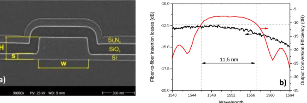
Silicon nano-rib waveguides with width, height and slab height of 500 nm, 210 nm and 50 nm, respectively, have been fabricated in a BiCMOS foundry using 248-nm lithography. At a dis-tance of 350 nm from the waveguide, doped regions have been introduced through implanta-tion of boron and arsenic with concentraimplanta-tion of 1018 cm-3 for the p- and n- regions, respec-tively. A scanning electron microscope (SEM) image of the waveguide cross-section is shown in Fig. 1(a).
The propagation losses, length, TPA coefficient and nonlinear coefficient of the waveguide under test are 1 dB/cm, 4 cm, 0.5 cm/GW and 280 W-1·m-1, respectively. More detailed
infor-mation about the fabrication and structure of the waveguides can be found in [11].
1540 1544 1548 1552 1556 1560 1564 -20.0 -17.5 -15.0 -12.5 -10.0 F ib e r-to-f ibe r i n s e rt ion lo ss es (d B ) Wavelength 11,5 nm -35 -30 -25 -20 -15 -10 -5 Out p ut Co nv er si o n Ef fi c ien cy ( d B) a) b)
Fig. 1. (a) SEM picture of the cross-section of a silicon nano-rib waveguide: width W= 500 nm, height H= 210 nm and slab height s= 50 nm. (b) Fiber-to-fiber insertion losses and conversion efficiency bandwidth (pump at 1552 nm) as a function of the signal wavelength.
The in- and out-coupling is achieved through standard 1D vertical grating couplers with insertion losses of 4.5 dB per coupler at 1550 nm and coupling angle of 9◦. The grating couplers
have a 3-dB bandwidth of around 35 nm centered in the 1550-nm region. The measured fiber-to-fiber insertion loss is shown as a function of wavelength in Fig. 1(b). Its value obtained for low power operation is around 13 dB in the wavelength region of interest. Remark that the use of more optimized grating coupler structures would allow reducing coupling losses to values as low as 0.62 dB per coupler [13] and therefore significantly decrease the overall insertion losses. In order to choose the frequency window for the phase-sensitive investigation, the conversion efficiency (CE) bandwidth of the waveguide was firstly characterized when applying 20 V of reverse bias and spanning a 35-nm range around the pump wavelength (1552 nm) with a CW
signal. The CW pump and signal powers launched into the waveguide were 18.5 dBm and
−15 dBm, respectively. The output CE, defined as the ratio between idler and signal power at
the output of the waveguide is reported in Fig. 1(b), showing a maximum of −7.5 dB and a 3-dB bandwidth of around 11.5 nm. No dispersion optimization was performed for this particular waveguide. Proper dispersion engineering of the waveguide is expected to result in a wider CE bandwidth. However the available bandwidth was sufficient for the present demonstration.
3. Static characterization of the phase sensitive extinction ratio
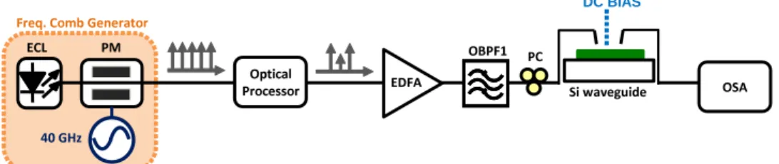
The setup used for the static characterization is sketched in Fig. 2. A continuous wave signal emitted at 1549.76 nm by a narrow linewidth (∼100 kHz) external cavity tunable laser source (ECL) was phase modulated (PM) with a 40-GHz RF signal with a modulation index (defined as the ratio of the peak-to-peak voltage of the driving signal to the half-wave voltage of the phase modulator) of 4.0 in order to generate an optical frequency comb with 40-GHz line spacing.
ECL PM 40 GHz PC EDFA Optical Processor
Freq. Comb Generator
DC BIAS
Si waveguide OBPF1
OSA
Fig. 2. Experimental setup for static characterization of the phase-sensitive properties of the silicon waveguide with reverse-biased p-i-n junction.
An optical processor was then used to select three neighboring comb lines: the outer ones act as pumps and the central one serves as signal [12]. The choice of a pump-signal separation of 40 GHz has been dictated by the available frequency comb generator as well as by the ability to sufficiently attenuate the undesired frequency components. The pumps power levels were then equalized and the pump-to-signal power ratio set to 30 dB in order to avoid the onset of saturation effects. Pumps and signal were amplified with an erbium-doped fiber amplifier (EDFA) followed by an optical band-pass filter (0.8-nm full-width at half-maximum bandwidth) to suppress the out-of-band amplified spontaneous emission (ASE) noise. The three waves were injected into the waveguide through a vertical grating coupler after aligning their states-of-polarization to the TE mode of the device. A reverse-bias voltage of 20 V was applied to the p-i-n junction for free-carrier removal. At the output of the waveguide, the signal power was measured using an optical spectrum analyzer (OSA) as the relative phase of the signal with respect to the phases of the pumps was changed using the optical processor.
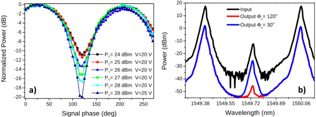
The dependence of the normalized output signal power on the signal phase is reported in Fig. 3(a) for total input power levels at the waveguide grating spanning from 24 dBm to 28 dBm and corresponding to effective powers coupled in the waveguide between 16.5 dBm and 20.5 dBm per pump.
As can be seen in Fig. 3(a), once the applied voltage is kept constant at 20 V, the phase-sensitive ER increases with the pump power from 10.8 dB to 16.7 dB. Furthermore, increasing the voltage applied to the junction to 25 V enables increasing the ER up to 20 dB (for 20.5 dBm of power per pump). Comparison between input spectrum and output spectra for maximum “amplification” (Φs= 30◦) and “de-amplification” (Φs= 120◦) are reported in Fig. 3(b), clearly
0 50 100 150 200 250 -20 -18 -16 -14 -12 -10 -8 -6 -4 -2 0 No rmal iz ed Po wer (dB )
Signal phase (deg)
PT= 24 dBm V=20 V PT= 25 dBm V=20 V PT= 26 dBm V=20 V PT= 27 dBm V=20 V PT= 28 dBm V=20 V PT= 28 dBm V=25 V 1549.38 1549.55 1549.72 1549.89 1550.06 -50 -40 -30 -20 -10 0 10 20 P o we r (dB m ) Wavelength (nm) Input Output Φs= 120 o Output Φs= 30 o a) b)
Fig. 3. (a) Normalized phase-sensitive gain as a function of the signal phase for various total power levels at the input vertical grating coupler and p-i-n junction reverse-biased either at 20 V or at 25 V. (b) Spectra at the input and output of the waveguide for maximum and minimum output signal power with 28 dBm of total input power and 25 V of reverse-bias applied.
4. System experiment
Figure 4 shows the changes in the static characterization setup of Fig. 2 made in order to inves-tigate the scheme under dynamic conditions, i.e. with a DPSK-modulated signal.
ECL PM OBPF2 40 GHz Feedback loop PC Pre-amplified Balanced Receiver OBPF3 EDFA APD 10 dB SMF Optical Processor EDFA Freq. Comb Generator
Phase stabilization feedback
DC BIAS Si waveguide PM Noise emulation PZT Bit Pattern Generator OBPF1
Fig. 4. Experimental setup for dynamic phase regeneration of a 10-Gb/s DPSK signal.
The optical processor was used to separate the signal from the pumps after the frequency comb generator by outputting it to a different port so that it could be modulated in the DPSK format at 10 Gb/s using a standard Mach-Zehnder modulator (MZM) driven in push-pull oper-ation by a non return-to-zero pseudo-random binary sequence (PRBS) of length 215
− 1. The
pumps were propagated through 13.5 m of standard single mode fiber (SMF) and coupled back together with the signal via a 3-dB coupler. The length of SMF was chosen in order to approx-imately match the pumps and signal path lengths, therefore easing the operation of the phase control loop aiming at compensating for slow thermal drifts. A polarization controller (PC) in each arm was used to align the state-of-polarization of pumps and signal to the TE mode of the waveguide.
After coupling back together the three waves, they were amplified to a total power of 24 dBm, band-pass filtered and injected into the Si-waveguide. A relatively low input power had been chosen for this proof-of-principle experiment to minimize coupling drifts due to thermal effects in the waveguide. Using a temperature controlled stage would allow increasing the power and therefore better performances would be expected. The waveguide junction was reverse-biased
with 25 V in order to keep the overall insertion losses, including nonlinear losses, around 14 dB. At the waveguide output, a pair of optical bandpass filters (OBPFs) with 0.8-nm and 0.3-nm bandwidths, were used to select the signal and input it to the pamplified DPSK balanced re-ceiver for BER testing. A second EDFA located between the OBPFs was used to compensate for extra insertion losses. Finally, phase-to-intensity demodulation in the receiver was performed by a 1-bit (100 ps) delay interferometer followed by a balanced photodiode with cut-off fre-quency of 45 GHz and an electrical low-pass filter with a bandwidth of 7.5 GHz.
The splitting of pumps and signal and their propagation along different paths inevitably re-sults in a loss of phase coherence due to thermal effects, even when balancing the paths lengths. In order to lock the waves in phase, 10% of the signal power was detected by a slow speed avalanche photodiode (APD) after the OPBFs following the waveguide and used as a refer-ence for a feedback loop based on a piezoelectric actuator (PZT). The PZT has a bandwidth of 15 kHz and therefore is able to compensate for the slow thermal drift between the waves.
5. Regeneration results
In order to investigate the regeneration properties of the scheme, phase noise was emulated deterministically by adding sinusoidal phase modulation to the DPSK signal using a phase modulator (PM) driven by a single RF tone generated from an independent unsynchronized RF source. The modulation index and the frequency of the noise tone have been varied to verify the effectiveness of the regenerator under different operation conditions.
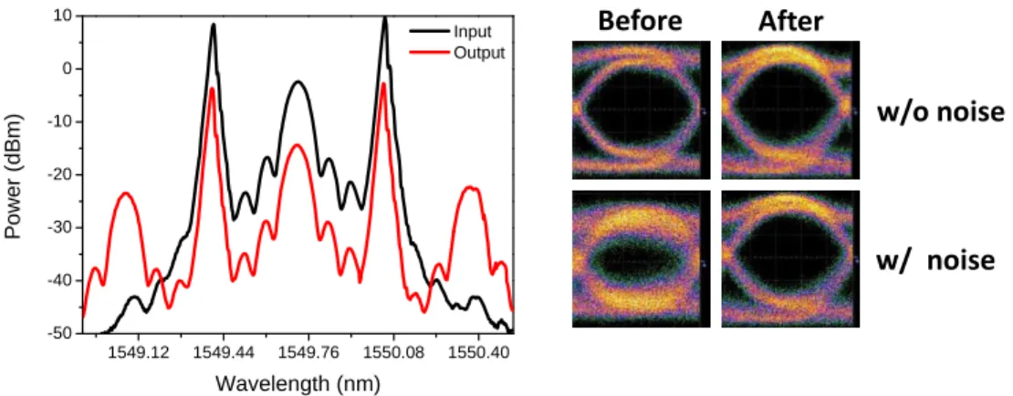
Spectra at the input and output of the waveguide are reported in Fig. 5(a) together with eye diagrams in Fig. 5(b) before and after regeneration under two test conditions: when no driving signal is applied to the PM (“w/o noise”) and when the phase noise is emulated by a 5-GHz RF signal with a modulation index of 0.57 (“w/ noise”).
1549.12 1549.44 1549.76 1550.08 1550.40 -50 -40 -30 -20 -10 0 10 P o we r (dB m ) Wavelength (nm) Input Output
Before
After
w/o noise
w/ noise
Fig. 5. (a) Optical spectra at the input and output of the waveguide under dynamic operation with a 10-Gb/s DPSK signal. (b) Eye diagrams at the receiver for −36 dBm of received power before (left) and after (right) regeneration, without (top) and with (bottom) phase noise generated by a 5-GHz tone with a modulation index of 0.57.
Clear and open eye diagrams can be seen after the regeneration with little distortion com-pared to the back-to-back reference signal with no noise added, and a significant improvement compared with the back-to-back signal with additional phase noise.
In order to properly assess the performance of the regenerator, the bit-error-ratio (BER) of the signal before and after regeneration was measured for no degradation as well as phase noise frequencies of 4 GHz, 5 GHz and 6 GHz. All the measurements have been carried out keeping the modulation index of the phase noise fixed at 0.57. The resulting BER curves as a function
of the received power are shown in Fig. 6(a). 0.0 0.2 0.4 0.6 0.8 0 2 4 6 8 10 12 14 16 18 60 Po wer pen al ty (dB )
Noise modulation index (Vpp/Vπ) Before regeneration After regeneration +Inf -46 -44 -42 -40 -38 -36 -34 -32 -30 -28 11 10 9 8 7 6 5 4 3 2
Before After reg. No noise 4 GHz noise 5 GHz noise 6 GHz noise -lo g (BE R) Prec (dBm) a) b)
Error floor at BER= 10-3
Fig. 6. (a) BER as a function of the received power for different phase noise loading con-ditions before (solid symbols) and after (hollow symbols) regeneration. (b) Power penalty (compared to back-to-back for a BER=10-9) as a function of the modulation index of the 5-GHz radio frequency tone used to emulate the phase noise.
In the absence of added noise, the scheme results in a power penalty of around 1 dB with respect to the back-to-back reference taken at the PM output. However, when phase noise is added to the signal, the regenerated output shows an improved receiver sensitivity (defined at a BER= 10-9) for all the three considered phase noise frequencies, enabling to decrease the power penalty from 10 dB down to less than 3.5 dB. Increased stability both in terms of phase coher-ence and coupling drifts is expected to allow decreasing the implementation penalty further. Notice that the different performances measured for the different phase noise emulation fre-quencies without regeneration are caused by the electrical low-pass filter at the receiver. The roll-off of the filter transfer function partially compensates for the degradation caused by the added phase noise. This compensation is indeed stronger the closer the noise frequency is to the 3-dB bandwidth of the filter, therefore resulting in better BER performances for 6-GHz noise emulation compared to 4 GHz. While this effect can be clearly detected on the BER of the signal before regeneration, no significant correlation can be seen between the performances of the regenerated output and the frequency chosen for the noise emulation.
The last aspect that was investigated is the impact of the modulation index on the regeneration performances for a fixed noise frequency (5 GHz). The power penalty at BER= 10-9with respect to back-to-back without degradation is reported in Fig. 6(b) as a function of the modulation index, before and after regeneration.
The results show that an increase of the phase noise modulation index slowly increases the power penalty for the regenerated signal. The degradation however grows far steeper on the signal without regeneration, leading to an error floor at a BER of 10-3 when the modulation index of the RF tone reaches 0.78. The corresponding regenerated signal can achieve error-free performances with a penalty below 6 dB.
6. Conclusions
We have demonstrated for the first time phase regeneration for DPSK signals using a sili-con waveguide with a reverse-biased p-i-n junction as nonlinear medium and sili-continuous-wave pumping. The phase-sensitive properties of the waveguide have been statically (i.e. under CW operation) investigated, reporting phase-sensitive ERs reaching 20 dB. The performances of the phase regenerator have been investigated for a 10-Gb/s DPSK signal under various phase-noise
loading conditions. Both frequency and modulation index of the deterministic RF tone used to emulate phase noise on the signal have been varied, with the regenerator allowing an improve-ment in the receiver sensitivity in all the cases investigated, achieving error-free performances (BER 10-9) even for a degraded signal showing an error floor at a BER of 10-3.
Acknowledgments
This work was partially funded by the German Research Foundation (DFG) in the framework of Sonderforschungsbereich SFB787. Financial support from the Danish Research Council for Technology and Production Sciences (project 09-066562) and from Villum Fonden via the NATEC Centre is acknowledged.