Any correspondence concerning this service should be sent to the repository administrator:
[email protected]
To link to this article:
DOI:10.1016/j.diamond.2012.05.007
http://dx.doi.org/10.1016/j.diamond.2012.05.007
This is an author-deposited version published in:
http://oatao.univ-toulouse.fr/
Eprints ID: 6482
To cite this version:
Koné, Sodjan and Schneider, Henri and Isoird, Karine and Thion, Fabien and
Achard, Jocelyn and Issaoui, Riadh and Msolli, Sabeur and Alexis, Joël An
assessment of contact metallization for high power and high temperature
diamond Schottky devices. (2012) Diamond and Related Materials, vol. 27-28 .
pp. 23-28. ISSN 0925-9635
O
pen
A
rchive
T
oulouse
A
rchive
O
uverte (
OATAO
)
OATAO is an open access repository that collects the work of Toulouse researchers and
makes it freely available over the web where possible.
An assessment of contact metallization for high power and high temperature
diamond Schottky devices
☆
S. Koné
a,b, H. Schneider
a,b,⁎
, K. Isoird
a,b, F. Thion
a,c, J. Achard
d, R. Issaoui
d, S. Msolli
e, J. Alexis
eaCNRS, LAAS, 7 avenue du Colonel Roche, F-31077 Toulouse, France bUniversité de Toulouse, UPS, INSA, INP, ISAE, LAAS, F-31077 Toulouse, France
cCNRS, Laboratoire ampère, INSA-Lyon, 20, avenue Albert Einstein, F-69621 Villeurbanne, France dCNRS, LSPM, Université Paris 13, 99 av. JB Clément, F-93430 Villetaneuse, France
eCNRS, LGP, ENI-TARBES, 47, avenue d'Azereix BP 1629, F‐65016 Tarbes, France
a b s t r a c t
Keywords: Diamond
Power semiconductor devices Schottky contact
Device characterization
Different metals W, Al, Ni and Cr were evaluated as Schottky contacts on the same p-type lightly boron doped homoepitaxial diamond layer. The current–voltage (I–V) characteristics, the series resistance and the thermal stability are discussed in the range of RT to 625 K for all Schottky devices. High current densities close to 3.2 kA/cm2are displayed and as the series resistance decreases with increasing temperature, proving the
potential of diamond for high power and high temperature devices. The thermal stability of metal/diamond interface investigated with regards to the Schottky barrier height (SBH) and ideality factor n fluctuations in-dicated that Ni and W are thermally stable in the range of RT to 625 K. Current–voltage measurements at re-verse bias indicated a maximum breakdown voltage of 70 V corresponding to an electric field of 3.75 MV/cm. Finally, these electrical measurements have been completed with mechanical adhesion tests of contact met-allizations on diamond by nano-scratching technique. These studies clearly reveal Ni as a promising contact metallization for high power, high temperature and good mechanical strength diamond Schottky barrier diode applications.
1. Introduction
Due to its exceptional properties, diamond is a very attractive ma-terial for power electronic switch devices. Its high electric breakdown field (Ec~ 10 MV/cm), high carriers mobilities (2200 cm2/V.s for
elec-trons[1]and 2200 cm2/V.s for holes[2]) and low dielectric constant
(εr~ 5.7) are suitable for high power and high frequency applications.
In addition, the high bandgap (Eg~ 5.5 eV) and the unique thermal
conductivity (20 W/cm.K) of diamond can be well exploited for a wide field of high temperature applications. Recent advances in syn-thesis of electronic grade single crystal intrinsic and boron doped di-amond by chemical vapor deposition have unlocked the way to the development of diamond technologic processing for power electronic devices. This includes the steps of polishing, RIE etching, electrical contacts and edge termination structures. Among those steps, mas-tering electrical contacts on diamond is definitely a major issue. To date, ohmic contacts are obtained in a reproducible way on p-type boron doped diamond by depositing Ti/Pt/Au[3]and Si/Al[4]with
low contact resistivity, around 10− 6Ω.cm2, which is in agreement
with electronic devices application requirements. However, studies on rectifier contacts in the literature face the difficulty to find suitable metals which form high Schottky barrier height, yield good mechan-ical adhesion and high thermally stable interface to diamond.
In this work, different metals W, Al, Ni and Cr were evaluated as Schottky contacts on the same lightly boron doped homoepitaxial diamond layer. The current–voltage (I–V) characteristics, the series resistance and the thermal stability are discussed in the range of RT to 625 K for all Schottky devices. Besides these electrical measure-ments, mechanical adhesion of contact metallizations on diamond is also investigated by nano-scratching technique.
2. Device test processing
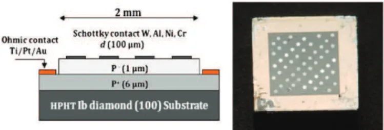
p+and p−-type boron doped homoepitaxial diamond layers have
been grown on 3 × 3 mm2HPHT Ib(100) diamond substrate. To
pre-pare the substrate's surface prior to growth, a H2/O2plasma etching
pre-treatment has been performed[5]. Since the use of high micro-wave power densities strongly limits boron incorporation[6], medi-um microwave power (1500 W) and a pressure of 80 mbar have been used to deposit the 6 μm-thick heavily boron doped diamond layer (p+) at a B/C ratio in the gas phase of 2000 ppm. The 1
μm-thick p−
‐layer was then deposited at a microwave power of 3000 W
☆ Presented at the Diamond 2011, 22nd European Conference on Diamond, Diamond‐Like Materials, Carbon Nanotubes, and Nitrides, Budapest.
⁎ Corresponding author at: CNRS, LAAS, 7 avenue du Colonel Roche, F-31077 Toulouse, France. Tel.: +33 5 61 33 69 96.
E-mail address:[email protected](H. Schneider).
and a pressure of 100 mbar and a B/C ratio reduced down to a few ppm. The resulting film was free of non-epitaxial crystals and SIMS measurements indicate a boron doping of 4 · 1020cm− 3 and
3 · 1017cm− 3respectively in p+and p−-layers (Fig. 1).
By selective RIE etching, a 2 × 2 mm2p−-drift layer was insulated
in the center of the substrate. Then, Ti/Pt/Au ohmic contact was de-posed around the p−-layer on the etched out area (p+
-layer) and annealed at 500 °C under nitrogen flow for 1 h. Finally, circular Schottky contact metallizations W, Al, Ni, and Cr of 100 μm diameter were evaporated on the top of lightly B-doped layer by a same photo-lithography process (lift-off technique). Prior to each photolithogra-phy process, the p−-area sustained a chemical cleaning consisting
in acetone, trichloroethylene and oxygen O2plasma treatment after
water rinsing. Such cleaning process is effective to remove any organ-ic contamination. Deposition of various Schottky metals on a same sample is very demanding technologically, but this solution provides the advantage to overcome reproducibility problems of diamond layers obtained by chemical vapor deposition (dislocations density, doping, thickness…). Thus, the characteristics obtained can be more easily correlated to metals.Fig. 2shows the cross section and photography of the carried out structure with W (15 SBD devices), Al (12 SBD de-vices), Ni (12 SBD devices) and Cr (13 SBD devices) on the top of the p−central area.
3. Results and discussion
3.1. Current–voltage characteristics from 300 K to 625 K
The current–voltage characteristics of Schottky devices were per-formed with an Agilent HP4142B analyzer from RT to 625 K. About half of the devices showed linear characteristics or excessively high reverse currents depending on their location on the p−-area mostly
due to bulk defects (dislocations) which induce leakage paths in ma-terial[7,8]and near surface homogeneously distributed defects across the Schottky contact area which act electrically as highly doped and low barrier height regions[9]. Here we present the best results that were achieved for each type of contact metallization (Fig. 3).
Very high current densities in the range of 1600 A/cm2
–3200 A/cm2 are found for Ni/diamond Schottky device at 5 V bias voltage in
Fig. 3a. The changes in current–voltage (I–V) characteristics with tem-perature increase can be discussed in two separate phases depending on the competition between dopants activation process and thermal fall of carrier mobility. In the first step from RT to 525 K, the gradual thermal ionization of dopants outweighs the carrier mobility drop with temperature increase. Thus, the current density increases up to 3.2 kA/cm2at 525 K corresponding to the point of complete ionization
of dopants.
In the second step (beyond 525 K), all dopants are ionized, the level of current output is then governed by the carrier mobility drop with temperature. Here, the current density goes down to 2.9 kA/cm2at
625 K. As far as the reverse operation is concerned, the Ni/diamond Schottky device shows very low reverse leakage current levels and no significant change can be noted in their thermal activation in the inves-tigated temperature range.
For W/diamond Schottky device inFig. 3b, an increase in current density from 550 A/cm2to 1000 A/cm2at 5 V bias voltage is revealed.
In such contact metallization, a high resistivity to the current flow through most devices could be clearly observed compared to Ni/diamond devices. However, all of them yielded very low reverse leakage cur-rent levels as well as Ni contacts.
OnFig. 3c, high current densities from 600 A/cm2to 1300 A/cm2 are highlighted at 5 V bias voltage in Al/diamond devices and very low reverse leakage currents are displayed up to 575 K where one can see the reverse current increases in ×3 orders of magnitude. This be-havior has been also observed in other Al devices. Such sudden degra-dation of reverse leakage current, due to a hard break of the Schottky barrier height, could be explained by the formation of a carbide layer at the Al/diamond interface. Indeed, Al is one of the well-known metals reacting easily with diamond at temperature and forming a carbide layer (aluminum carbide Al4C3). Few tens of nanometers of such layer
are generally enough to change the carrier transport of Schottky barrier diodes[10].
As shown inFig. 3d, the Cr/diamond device provides high current densities ranging from 1400 A/cm2to 3800 A/cm2at 525 K. But, these
devices mostly displayed a chaotic evolution in (I–V) characteristics with an increase of temperature and high leakage current levels com-pared to other contact metallizations.
3.2. Devices series resistance as function of temperature
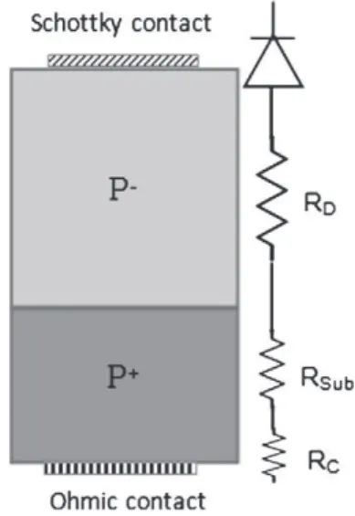
Another important property of a diode is its on-state series resis-tance RonS responsible for voltage drop across the device when forward
biased. It should be as low as possible.Fig. 4shows the electrical model of a Schottky barrier diode. The on-state voltage drop VFacross the
de-vice is the sum of the voltage drop due to the Schottky contact rectifying effect and voltage drops due to the low doped drift area (p−-layer)
re-sistance RD, the substrate (p+-layer) resistance Rsuband the ohmic
con-tact resistance RC.
The on‐state voltage drop VFacross the device is given by:
VF¼ kT q ⋅ ln JF JS ! þ Rð Dþ Rsubþ RCÞ⋅JF ð1Þ
where JF and JSare the forward current and the saturation current
densities respectively.
The heavily doped p+-layer is known as a very low resistive area.
Moreover, the Au/Pt/Ti/diamond ohmic contact resistance is typically in the range of 10− 6Ω.cm2.
Therefore, the on-state series resistance RonS across the device can
be considered as mainly due the low doped drift area resistance RD. It
is measured here as a function of temperature from the dynamic
Fig. 1. SIMS profile in the lightly and the heavily B-doped diamond layers.
Fig. 2. Cross section and photography of the fabricated SBD device structure with W, Al, Ni, and Cr Schottky contacts on the top of the p−central area.
resistance extracted from the slope of (I–V) characteristics for each kind of Schottky metallizations.Fig. 5shows each experimental data plotted as a function of temperature.
As one can note, the on-state resistance RonS decreases with an
in-crease of temperature for all devices. Due to the deep boron acceptor level in diamond with an activation energy of 0.37 eV for boron con-centrations well below the metal–insulator transition, only a small fraction of dopants is ionized at room temperature, making semicon-ductor diamond a poor electrical consemicon-ductor at low temperature. The dopants ionization rate depending on the temperature, the more the temperature increases, the more the series resistance RonS decreases.
Otherwise, the series resistance differs depending on the Schottky metallization. This difference is probably related to the inhomogene-ity of the active region (doping, dislocations, thickness…) and/or the difference in experimental SBH. It is therefore difficult to draw con-clusions related to the type of metallization even when the nickel Ni de-vice yields the lowest on-state series resistance RonS while the tungsten
W is the most resistive.
3.3. Thermal stability of contacts metallizations on diamond
For high temperature applications, the thermal stability of metal/ semiconductor interfaces is the main requirement for power electron-ic develectron-ices. The thermal stability has been investigated in the range of 300 K–625 K for each Schottky metallization regarding the Schottky barrier height (SBH) and the ideality factor (n) extracted from the current–voltage characteristics.
Fig. 3. Current–voltage (I–V) characteristics in the range of RT–625 K for Ni/diamond, W/diamond, Al/diamond and Cr/diamond SBD devices.
Fig. 4. Electrical modeling of Schottky barrier diode.
The current transport mechanism in a Schottky barrier diode is governed by the thermionic emission (TE). The corresponding current– voltage (I–V) curve can be described by:
J ¼ Js exp qV nkT ! −1 " # Js¼ AT2S exp −qΦΒ kT ! ð2Þ
where Jsis the saturation current density, n is the ideality factor, A* is the
Richardson constant (96 A/cm2.K2
), qΦBis the Schottky barrier height
(SBH) and S is the Schottky contact area.
For each temperature, the Schottky barrier height (SBH) was cal-culated from the saturation current density Jsdetermined by
extrap-olating the semilog forward (I–V) curve in the linear region at zero bias (V = 0) and the ideality factor (n) from the slope (a) of the ex-panded (I–V) curve according to Eqs.(3) and (4).
n ¼ q kT⋅ 1 a ð3Þ ΦΒ¼ kT q ⋅ ln AT2 JS ! ð4Þ
Fig. 6shows experimental data plotted as functions of tempera-ture for each kind of Schottky metallization.
As the ideality factor is far above one (n ≫1) in Al and Cr Schottky contacts, other carrier transport mechanisms interfere at the metal/ diamond interface in addition to the thermionic emission. Indeed,
tunneling and generation-recombination processes can occur through a Schottky contact in the case of extended defects and recombination centers in the space charge region respectively. These parasitic phe-nomena combine with interface traps density[11,12]are mainly re-sponsible for barrier loss in Schottky rectifiers. Evidently in our case of study, a large gap occurs between the experimental and the theoretical SBH expected for Al and Cr contacts. The decrease of the ideality factor with increasing temperature is known as carrier transport process tran-sition to thermionic emission exclusively, feature current transport mechanism in Schottky contacts[13].
In contrast, the ideality factor is extremely close to unity (n ≈1) for W and Ni contacts and almost insensitive to temperature increase. This means that the current transport mechanism in these contacts is basically thermionic emission process. Moreover, the SBH stability indicates an insignificant chemical reactivity of W and Ni contacts to diamond. Thus, these contact metallizations can be considered as thermally stable in the range of 300 K–625 K.
3.4. Reverse bias voltage measurements
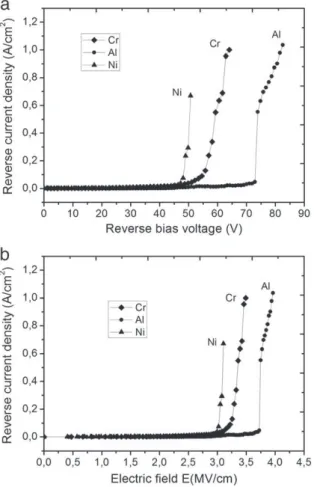
Current–voltage measurements at reverse bias have been per-formed immersing the sample in an insulating liquid (fluorine FC40). The insulating liquid avoids any electric field crowding at Schottky con-tact edges causing premature breakdown of the device. The results inFig. 7attest a maximum breakdown voltage VBRnear 50 V, 55 V and
70 V for Ni, Cr and Al contacts respectively. There is no correlation be-tween the type of metallization and the SBD devices reverse operation limit given the uncertainty on the active layer homogeneity (thickness, doping and dislocations density).
Fig. 6. The ideality factor (a) and the SBH (b) for W, Al, Cr and Ni Schottky contact to diamond as functions of temperature.
Fig. 7. Diamond SBD devices reverse operation limit as a function of: a) voltage, b) electric field.
Considering a triangular field distribution within the uniformly doped P−-layer, the breakdown voltage (V
BR) and the corresponding
electric field (Emax) for unipolar power devices can be related by[14]:
VBR≈ εs⋅E2max
2qNA ð5Þ
where εsis the dielectric constant (F/cm− 2), Emaxis the maximum
electric breakdown field (V/cm), q is the elementary charge (C), and NAis the doping of p−-layer.
From Eq.(5), a maximum breakdown electric field of 3.75 MV/cm was calculated for the Al/diamond SBD device. This performance indi-cates that our diamond crystalline grade is in good agreement with the current state-of-the-art in CVD growth of single crystal diamond. Indeed, the growth of high quality single crystal CVD diamond meet-ing power electronic devices applications requirements still remains an important challenge. Consequently, practical performances of dia-mond based electronic devices are well below the theory. In the case of single crystal diamond SBDs in the literature, high reverse current levels are frequently observed and the maximum electric breakdown field does not exceed 4 MV/cm[15,16].
3.5. Schottky contacts adhesion on diamond
A good mechanical adhesion is also a major property for metal/ semiconductor contacts. It is a key requirement for device bonding process and packaging technologies.
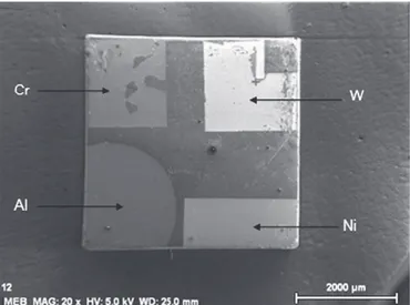
The Schottky contact metallizations studied above were deposited on a diamond sample by the same photolithography process previ-ously described.Fig. 8shows a photography of Cr, W, Ni and Al coat-ings on diamond sample.
The mechanical strength of metal coatings on diamond sample was investigated by nanoscratching technique at the Production Engi-neering Research Laboratory (LGP-Tarbes, France). Nanoscratching test is based on making scratches on the sample surface by moving a Berkovitch tip (indenter) in three successive steps and measuring their depth. This gives an opportunity to evaluate the hardness of coatings qualitatively.
♦ The first run of the indenter with a very low normal force applied (100 μN) determines the metal coating topography.
♦ The second run in which the applied force increases gradually until the maximum force imposed permits to evaluate the hard-ness of the metal coating.
♦ The third run in scratch background with the lowest applied force determines the metal coating spring back after scratching and the topography of the scratch sidewall.
The tests were carried out with a scratch speed of 10 μm/s, an im-posed maximum force of 40 mN and a scratch distance of 200 μm. The indenter penetration curves as functions of scratch distance and the background from scratches are presented respectively inFig. 9a and b for W, Al, Cr and Ni coatings.
Considering the scratch depths' importance inFig. 9a, Al and W coatings seem to be less resilient to scratching. More specifically, tung-sten contact behavior to scratching differs from other contact metalliza-tions inFig. 9b. Indeed, interfacial and structural disintegrations occur into the coating at low applied loads while no disintegration is observed in other coatings.
Furthermore, because of their low hardness, plastic deformations were observed in all coatings during the second run of the indenter as the normal force applied gradually increased.
However, the adhesion on diamond is stronger than the elasticity limit in the case of Ni, Cr and Al coatings. Also, scratch background in-spections indicate that the mechanical dissipation in Cr and W coat-ings seems lower than in the Ni and Al coatcoat-ings. In fact, cracks were observed on scratch sidewalls in the case of Cr and W coatings as shown inFig. 9b.
These observations reveal that Ni and Al contacts exhibit good adhesion on diamond.
Fig. 8. SEM photography of Cr, W, Ni and Al coatings on diamond.
Fig. 9. a) Indenter penetration curves as functions of scratch distance, b) background from scratches.
4. Conclusion
Table 1summarizes experimental data related to contact metalli-zation evaluated in the range of RT–625 K. The best results for each criteria investigated are marked in bold.
Compared with the other contact metallizations, all of the experi-mental data inTable 1indicate that nickel (Ni) is a suitable contact metallization for high power, high temperature and good mechanical strength diamond Schottky barrier diode applications.
In comparison to the state of the art of Schottky contacts on dia-mond, there is no work on mechanical adhesion and, moreover, the thermal stability is rarely investigated.
Thus, the only criteria for comparison that can be pointed here is the experimental Schottky barrier height (SBH).
Fig. 10displays some experimental SBH data from various studies
[7–22]. It is clear that our achievements are in good agreement with the state‐of‐the‐art of Schottky contacts on diamond.
Acknowledgments
This work has been supported by the Aerospace Valley Cluster and the French National Research Agency ANR through project no. Blanc-06-2-134411. The authors acknowledge the collaborative effort of the CNRS-LAAS RTB clean room team.
References
[1] N. Tranchant, M. Nesladek, D. Thomson, Z. Remes, A. Bogdan, P. Bergonzo, Phys. Status Solid 204 (9) (2007) 2827–3200.
[2] T. Teraji, K. Arima, H. Wada, Toshimichi Ito, Appl. Phys. Lett. 96 (10) (2004) 5906–5908.
[3] Y. Chen, M. Ogura, S. Yamasaki, H. Okushi, Semicond. Sci. Technol. 20 (2005) 860–863.
[4] M. Werner, C. Johnston, P.R. Chalker, S. Romani, I.M. Buckley‐Golder, J. Appl. Phys. 79 (1996) 2535.
[5] A. Tallaire, J. Achard, F. Silva, R.S. Sussmann, A. Gicquel, E. Rzepka, Phys. Status Solidi A 201 (2004) 2419.
[6] R. Issaoui, J. Achard, F. Silva, A. Tallaire, A. Tardieu, A. Gicquel, M.A. Pinault, F. Jomard, Appl. Phys. Lett. 97 (18) (2010) 3.
[7] R. Kumaresan, H. Umezawa, N. Tatsumi, K. Ikeda, S. Shikata, Diamond Relat. Mater. 18 (2–3) (February–March 2009) 299–302.
[8] Hitoshi Umezawa, Norio Tokuda, Masahiko Ogura, Sung-Gi Ri, Shin-ichi Shikata, Diamond Relat. Mater. 15 (11–12) (November–December 2006) 1949–1953. [9] A. Vescan, W. Ebert, T. Borst, E. Kohn, Diamond Relat. Mater. 4 (1995) 661–665. [10] M. Wade, P. Muret, F. Omnès, A. Deneuville, Diamond Relat. Mater. 15 (2006) 614. [11] J. Tersoff, W.A. Harrison, Phys. Rev. Lett. 58 (1987) 2367.
[12] W. Mönch, Europhys. Lett. 27 (1994) 479.
[13] Tokuyuki Teraji, Yasuo Koide, Toshimichi Ito, Phys. Status Solidi RRL 3 (2009) 211. [14] L.M. Tolbert, B. Ozpineci, S.K. Islam, M.S. Chinthavali, Power Energy Syst., Proc.,
2003, pp. 317–321.
[15] A. Vescan, I. Dauville, P. Gluche, W. Ebert, E. Kohn, Diamond Relat. Mater. 7 (1998) 581–584.
[16] D.J. Twitchen, A.J. Whitehead, S.E. Coe, J. Isberg, J. Hammersberg, T. Wikström, E. Johansson, IEEE Trans. Electron. Devices 51 (5) (May 2004) 826–828. [17] J. Butler, M.W. Geis, K.E. Krohn, J. Lawless, S. Deneault, Semicond. Sci. Technol. 18
(2003) S67–S71.
[18] Y.G. Chen, M. Ogura, H. Okushi, N. Kobayashi, Diamond Relat. Mater. 12 (2003) 1340–1345.
[19] M. Craciun, Ch. Saby, P. Muret, A. Deneuville, Diamond Relat. Mater. 13 (2) (2004). [20] K. Ikeda, H. Umezawa, K. Ramanujam, S. Shikata, Appl. Phys. Expr. 2 (2009) 011202. [21] D. Takeuchi, S. Yamanaka, H. Okushia, Diamond Relat. Mater. 11 (2002) 355–358. [22] H. Umezawa, S. Shikata, 21st International Symposium on Power Semiconductor
Devices & IC's, ISPSD, 14–18 June 2009, IEEE, 2009, p. 259. Table 1
Experimental data related to Schottky contact metallization on diamond.
Contact metallization W Al Cr Ni
SBH (eV) ΦB 1.67 1.31 0.73 1.57
Threshold voltage (V) Vth 1.5 2.5 1 1.7
Current density range (A/cm2) Forward JF 550– 1000 600–1300 1400– 2800 1600– 3200 Reverse JR 10−7– 10−5 10−7 –10−5 10− 2–1 10−7– 10−5 Rectifying factor JF/JR 109 109 105 1010 Series resistance (mΩ.cm2) RonS 6.1– 3.85 3.54–2.04 2.81– 1.33 1.9– 1.07 Thermal stability Qualitative
analysis Good Good (≤300 °C) Poor Good Adhesion Qualitative analysis
Poor Good Fairly
good Good
Fig. 10. The state of the art of SBH from various metal/diamond Schottky contacts, (■) = literature, ( ) = this work.
![Fig. 10 displays some experimental SBH data from various studies [7–22]. It is clear that our achievements are in good agreement with the state‐of‐the‐art of Schottky contacts on diamond.](https://thumb-eu.123doks.com/thumbv2/123doknet/3604085.105735/7.892.49.427.148.597/displays-experimental-various-achievements-agreement-schottky-contacts-diamond.webp)