Vertical multilayer structures based on Porous
Silicon layers for Mid-InfraRed applications
M
AXIMED
URIS1,
M
OHAMMEDG
UENDOUZ1,
N
ATHALIEL
ORRAIN1,
P
ARASTESHP
IRASTEH1,
L
OÏCB
ODIOU1,
W
ARDAR
AIAH1,2,
Y
ANNICKC
OFFINIER2,
V
INCENTT
HOMY2ANDJ
OËLC
HARRIER1,*1
Univ Rennes 1, CNRS, Institut Foton – UMR 6082, F-22305 Lannion, France
2Institut d’Electronique, de Microélectronique et de Nanotechnologie (IEMN, UMR CNRS 8520),
Avenue Poincaré, BP 60069, 59652 Villeneuve d’Ascq, France.
Abstract: In this work, the fabrication of Porous Silicon Bragg reflector and vertical cavity
on P+ silicon substrate is investigated for applications in spectroscopic sensing in the Mid Infra-Red wavelength range. The complex refractive index of porous silicon layers is measured. Optical vertical devices are then fabricated and characterized by FTIR spectrophotometer. This work demonstrates the use of electrochemically prepared Bragg reflectors with reflectance higher than 95% and vertical cavity based on Porous Silicon layers operating in the Mid-IR spectral region (up to 8 µm). Experimental reflectance spectra of the vertical cavity structures are recorded as a function of air exposure duration after thermal annealing under nitrogen flux (N2)and results demonstrate that these structures could be used
for spectroscopic sensing applications in the Mid-IR field (2-8 µm) by grafting specific biomolecules on the porous silicon internal surface.
© 2018 Optical Society of America under the terms of the OSA Open Access Publishing Agreement 1. Introduction
Highly sensitive optical integrated sensors have received great interest during these last years [1-9]. In particularly, the ability to rapidly detect, identify and monitor chemical or biological species is imperative for environmental monitoring, health monitoring and security applications. The detection of traces of (bio)-chemical molecules requires sample preparation procedures combined with sophisticated analytical tools which can detect, within an acceptable time, disease biomarkers, emerging pollutants, chemical warfare agents or toxic industrial chemicals with high sensitivity to really detect low concentrations with high selectivity not to be affected by other factors in the environment. The sensor should also have a fast response and recovery time whilst being portable, easy to operate and produce data that are easily interpreted. A range of optical, electrochemical, fluorescence, electrical and spectroscopic technologies have been developed for the detection of different kinds of chemical molecules [10]. Although useful information can be obtained and the technologies have progressed significantly, it is recognized that these methods are not adequate in terms of both spatial and temporal resolution. A major challenge is also the need to increase sensing sensitivity and detection reliability.
In recent years, Infra-Red (IR) spectroscopy has been proven to be a simple, reliable, relatively fast and cost-efficient technique for analyzing complex samples and determining their composition. The sensor produces a spectrum which represents the molecular absorption or transmission, creating unique molecular fingerprint of the sample. It is used in several research and industrial areas, from quality control to forensic analysis [11-21]. The IR region of the electromagnetic spectrum can be divided into the near, mid and far IR regions. The
most common wavelength range for detection applications lies in the Mid Infrared (Mid-IR) region and particularly ranges between 2.5 μm and 15 μm (4000 - 670 cm-1). While current spectroscopic systems are based on bulk optical components, the resulting systems are large, expensive and not rugged. Photonic integrated circuits provide a route to small, low-cost and very rugged optical systems and could therefore be a game-changer for IR spectroscopic sensor systems. However, most integration technologies developed up to now are geared toward sub 2µm wavelength operation, which does not include the wavelength range of most interest for spectroscopic sensing, namely the mid-infrared.
The ability to tailor Porous Silicon (PSi) refractive index and layer thickness by controlling porosity and anodization etching time [22-24] makes it especially attractive for optical applications. Optical multilayer devices such as Bragg reflectors or micro-cavities have already been implemented from PSi layers notably for Visible and Near Infra-Red (NIR) wavelength ranges [25-29]. Two constant current densities are used for the High Porosity (HP) and Low Porosity (LP) layers with low and high refractive indices (nHP and nLP)
respectively for the fabrication of these optical devices. The etching times are adjusted to produce an optimized Bragg reflector or cavity with the resonant wavelength in the chosen spectral range.
Moreover, PSi is also biocompatible material and the functionalization of its internal surface by grafting molecules to detect is interesting for surface detection due to its high specific surface that is very important and up to 800 m2/cm3 [21, 22].
The implementation of a Mid-IR silicon photonics transducer with broad Mid-IR transparency (up to 8 µm by taking into account Si transparency) is a challenge that could find applications in spectroscopic sensing and environmental monitoring. This paper demonstrates the fabrication of vertical Porous Silicon multilayer structures on Si substrates and their potential in the Mid-IR wavelength range notably near the cut-off band of Si due to its absorption at 8 µm. That is why the fabrication of Bragg reflector and vertical cavity on P+ silicon substrate is investigated for applications in spectroscopic sensing in the (Mid-IR) wavelength range
2. Experimental conditions
The PSi layers were obtained by electrochemical anodization of p-type doped (100)-oriented silicon wafer (4-6 m.cm) at room temperature. The electrolyte was composed of HF(50%):ethanol: deionized water (2:2:1). The refractive indices and porosities of PSi single layers were studied by reflectometry in the near- and mid-infrared spectral ranges. Scanning electron miscroscopy (SEM) was used to obtain the thickness of PSi layers. The thickness of each porous layer was controlled by the anodization etching time. Current densities of 20 and 90 mA/cm2 were used for the low porosity (LP) and high porosity (HP) respectively. . These current densities were chosen to obtain a high index contrast.
The infrared reflectance spectra were measured by a Perkin Elmer Spectrum 100 FTIR spectrophotometer from 1.5 µm to 15 µm with a resolution of 4 cm-1. The calibration is performed by a measurement using a gold mirror with a calibrated reflection equal to 97.5% between 1.5 and 25 µm. The calibration protocol of the spectrometer takes into account absorption from the environment in particular absorption fringe of CO2, water vapor and
methane. From reflectance spectra, the complex refractive index of the fabricated single layers was deduced by fitting spectral fringes using the effective medium theory (Bruggeman model) [30, 31].
Some samples were annealed under N2 for 1 hour in order to desorb the specific surface of the
porous layers and to remove the contaminants.
From the refractive index and the anodization etching rate knowledge of the two studied PSi layers, the design of vertical optical devices was performed using the transfer matrix method
in order to determine the best combination of parameters for Bragg reflectors and cavities (reflection bandwidth, resonance wavelength and maximum reflectance).
3. Results and discussion
The porosities and associated Mid-IR refractive indices have been determined from reflectivity measurements of two single PSi layers whose fabrication parameters, given above in the experimental part, correspond to those of the multilayer structures. From the thicknesses measured by scanning electron microscopy, porosities and then complex refractive indices were determined by the adjustment of the calculated reflectance spectra of each PSi layer with experimental ones using Bruggemann model [32-34].
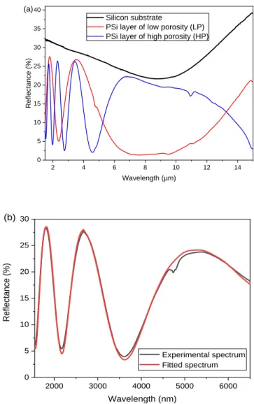
2 4 6 8 10 12 14 0 5 10 15 20 25 30 35 40 Silicon substrate
PSi layer of low porosity (LP) PSi layer of high porosity (HP)
Refle ctan ce ( %) Wavelength (µm) (a) 2000 3000 4000 5000 6000 0 5 10 15 20 25 30 Refle ctan ce ( %) Wavelength (nm) Experimental spectrum Fitted spectrum (b)
Fig. 1. (a) Experimental Mid-IR reflectance spectra of the PSi layer of high and low porosities and of the Si substrate. (b) Experimental and fitted reflectance spectra of the high porosity PSi
The experimental reflectance spectra are shown in Figure 1 (a) for the two PSi single layers obtained with the current densities of 20 and 90 mA/cm2. The experimental fringes are well visible until 8 µm before the silicon absorption in the Mid-IR range. The adjustment of the experimental spectra was carried out for wavelengths ranging from 2 to 8 µm. A good fit between experimental and theoretical spectra was obtained as illustrated in Figure 1 (b). The complex refractive indices and the extinction coefficients for the two PSi porosities are reported in Figures 2 (a) and (b), respectively.
1000 2000 3000 4000 5000 6000 7000 8000 9000 1,0 1,2 1,4 1,6 1,8 2,0 2,2 2,4
PSi layer of high porosity (HP) PSi layer of low porosity (LP)
Refr active ind ex Wavelength (nm) (a) 1000 2000 3000 4000 5000 6000 7000 8000 9000 10-4 10-3 10-2 10-1
PSi layer of high porosity (HP) PSi layer of low porosity (LP)
Extin ction Co efficien t Wavelength (nm) (b) Fig. 2. Variation of (a) PSi refractive index and (b) PSi extinction coefficient as a function of the
wavelength for the high and low porosity layers.
It should be noted that the extinction coefficient of porous layers is low in 1550 - 8000 nm spectral region as expected. The real refractive index contrast between the HP and LP films was found to be 0.88 at 1550 nm and 0.62 at 7 µm. The porosity values are respectively for the low and high porosities equal to 33 and 61 % and the extinction coefficient k is higher for the layer of lower porosity as indicated in Table 1 due to the contribution, of the Si absorption that is more important for this low porosity value.
Table 1. Physical parameters of the lower and higher PSi layers
Refractive index and
extinction coef. @ 1550 nm @ 7 µm Name of layer Value of porosity (%) n k n k LP 33 ± 6 2.35 ± 0.05 0.035 ± 0.004 2.07 ± 0.05 0.027 ± 0.004 HP 61 ± 4 1.47 ± 0.03 0.01 ± 0.002 1.45 ± 0.03 0.008 ± 0.002
In order to avoid the need for thick films in the multilayers devoted to mid-IR applications, a large index contrast was targeted between the layers forming the pattern. These values are therefore very promising for targeted applications considering the low absorption of the PSi layers.
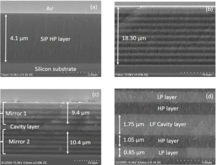
Fig. 3. SEM micrographs (cross sections) of (a) monolayer of PSi, (b) Bragg reflector structure and (c,d) vertical microcavity at some different scales.
Some examples of SEM micrographs of single layers (Figure 3(a)) and prepared multilayered structures such as Bragg mirror (Figure 3(b)) or vertical cavity (Figures 3(c) and figure 3(d)) are presented in Figures 3. The columnar structure of the porous layers is well observable in Figures 3(a) and (d). This morphology is characteristic of mesoporous layers that are fabricated from P+ Si substrate [21, 22]. The interfaces between individual layers as well as the surfaces of the multilayered structures were found to be smooth without any defect during the fabrication of thin film stacks (Figures 3(b), (c) and (d)).
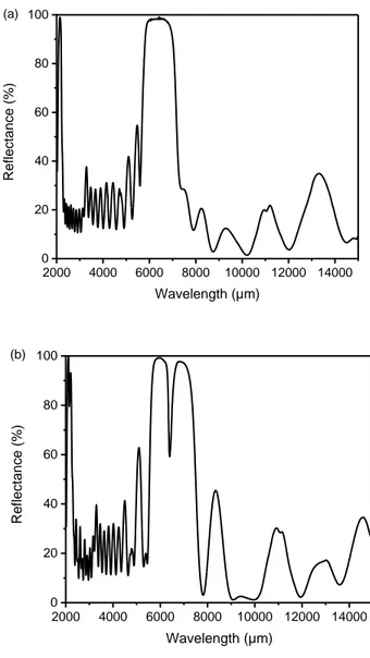
2000 4000 6000 8000 10000 12000 14000 0 20 40 60 80 100 Re flectance (%) Wavelength (µm) (a) 2000 4000 6000 8000 10000 12000 14000 0 20 40 60 80 100 Re flectance (%) Wavelength (µm) (b)
Fig. 4. Experimental reflectance spectra of (a) Bragg reflector and (b) vertical caviy structures.
The achieved reflectivity is determined by the number of layer pairs N and by the refractive index contrast n between the layers. The Bragg reflector is characterized by its central wavelength 0 (at normal incidence) and by the reflection bandwidth which is
determined mainly by the index contrast. These two parameters are defined respectively by the relationships (1) and (2).
nLPtLPnLHtLH
2 0 (1) n n 2 0 (2)with 2 n n n n n n HP LP HP LP
Where nHP(LP) and tHP(LP) are the refractive index and thickness of high (low) porosity
layers.
The thicknesses of pattern were fixed to obtain Bragg reflector and cavity structures centered at 6.5 µm. The experimental responses of the Bragg reflector is reported in Figure 4(a). The spectrum is centered close to 6560 nm. The experimental wavelength bandwidth is about 120 nm and the maximal reflectance is around 97%. The experimental spectrum is in close agreement with the theoretical spectrum taking the absolute errors into account. The absolute errors of measured refractive index and thickness of layers are 0.005 and 50 nm respectively.
This work demonstrates that it is possible to fabricate a Bragg reflector with good optical qualities in the Mid-IR range from P+ silicon substrates.
With the same pattern, a vertical cavity was fabricated with a resonance wavelength equal to 6550 nm. The experimental reflectance spectrum of the cavity is illustrated in figure 4(b). The resonance peak is close to the target value. Moreover, the reflectance value of the device of the bandwidth is as high as 97%.
Another merit factor is the quality factor of the structure. In order to study this parameter, we can use the Fabry-Perot classical model [35]. The quality factor is given by the following relationship:
L
R L R L n Q exp 1 2 exp 2 0 0 0 (3)where n0 is the refractive index of the defect layer that separates the two Bragg mirrors
(n0= 2.07), L its thickness 1.75 µm), 0 the expected resonant wavelength equal to 6560
nm, its absorption coefficient (2.3 cm-1) [36] and R the reflectance value equal to
97%by assuming that the two Bragg mirrors are similar.
For the elaborated microcavity, the theoretical quality factor is equal to 112 and from the experimental spectrum, the quality factor was estimated at around 60.
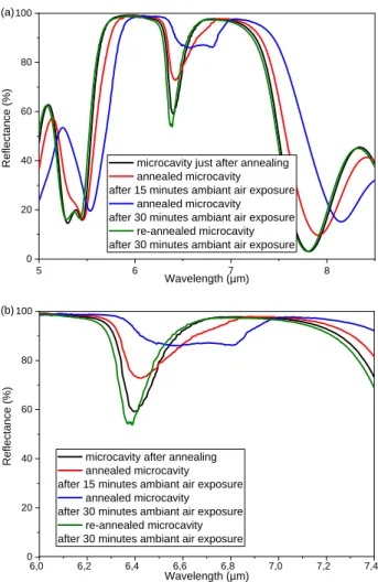
However, we noted a degradation of the quality factor as a function of time when the sample was exposed to air as shown in figures 5 . After thermal annealing under N2 at 300 °C for one
hour, the spectrum of initial experimental reflectance has been restored due to the desorption of the specific surface of the sample.
5 6 7 8 0 20 40 60 80 100 Refle ctan ce ( %) Wavelength (µm) microcavity just after annealing annealed microcavity after 15 minutes ambiant air exposure
annealed microcavity after 30 minutes ambiant air exposure
re-annealed microcavity after 30 minutes ambiant air exposure (a) 6,0 6,2 6,4 6,6 6,8 7,0 7,2 7,4 0 20 40 60 80 100 Refle ctan ce ( %) Wavelength (µm) microcavity after annealing annealed microcavity after 15 minutes ambiant air exposure
annealed microcavity after 30 minutes ambiant air exposure
re-annealed microcavity after 30 minutes ambiant air exposure (b)
Fig. 5. (a) Evolution of the experimental reflectance spectra of the same microcavity structure as a function of
exposure duration to air after annealing at 300°C of the structure under N2. (b) Evolution of the resonance
wavelength of the same microcavity structure as a function of exposure duration to air after annealing of the structure
under N2.
Several experimental reflectance spectra were recorded as a function of exposure duration to air after thermal annealing at 300°C under N2. These spectra are reported in Figure 5 (a).
We note a degradation of the cavity quality factor that is all the greater the longer the exposure of the micro-cavity to the ambient air. After a new heat treatment under N2 of the
cavity exposed to air for 30 minutes, the quality factor is again improved.
This quality factor reduction is better illustrated in Figure 5 (b) by showing the spectra near the resonance wavelength to emphasize the resonance FWHM and reflectance value increase.
The degradation of the quality factor is due to the adsorption on PSi internal surface of molecules contained in the ambient air. Indeed, molecules such as water vapor or methane have absorption lines in the studied wavelength range, around of 6550 nm.
A red shift is noted for the resonance peak and the width of the peak increases strongly due to the molecule adsorption with air exposure time. The initial reflectance is almost obtained after a new annealing under N2 of the 30 minutes – air exposed cavity (green curve
in figure 5 (b)). The difference between the two spectra (just annealing and new annealing after 30 minutes exposure) is due to the difference time between the FTIR measurement and the sample exit from the oven. Reflectance spectrum overlaps absorption bands of air
molecules and their detection is enhanced by the cavity [26-29]. So by a specific functionalization of porous silicon [24], these vertical optical structures could be used as transducers to detect low concentrations of target molecules by choosing the good resonance wavelength, in the Mid-IR range, and relative to its absorption band. However, such microcavities should be encapsulated in a neutral atmosphere so that a microfluidic system only interacts with a fluid containing molecules to be detected.
4. Conclusions
In conclusion, vertical multilayer stackings based on PSi layers were fabricated for Mid-IR wavelength range. From the experimental reflectance spectra of PSi thick layers, real and imaginary parts of the refractive index of these films of different porosities were obtained in the Mid-IR wavelength range. Bragg mirror and vertical cavity were then fabricated for notably near the cut-off band of Si due to its absorption at 8 µm. Multilayer structures based on PSi layers made from P+ Si substrates were then implemented. Maximal reflectance around 95% and a quality factor equal to 50 were obtained respectively for Bragg mirror and vertical microcavity. These optical devices could be used as highly sensitive transducers thanks to the PSi layers opened pores and wide internal surfaces. The first results obtained from these PSi multilayer structures can now serve as functionalized transducers by grafting biomolecules to develop spectroscopic sensing applications in the Mid-IR field (2-8 µm).
5. Funding and acknowledgments
Funding
This work was supported by the French national research agency under MID-VOC ANR project (ANR-17-CE09-0028-01). Equipments funding of Institut Foton were partly provided by the CPER Sophie.
Acknowledgments
Scanning Electron Microscopy imaging and porous silicon fabrication were performed in the CCLO - Renatech clean room facilities of Institut Foton.
References
1. K. Zinoviev,L.G. Carrascosa, J. Sánchez del Río, B. Sepúlveda, C. Domínguez and L.M. Lechuga, ”Silicon
photonic biosensors for lab-on-a-chip applications,” Adv. in Optical Technologies, 2008, 1-6 (2008).
2. R. Soref, ”The past, present, and future of silicon photonics,” J. of Selected Topics in Quantum Electronics
12, 1678–1687759 (2006)
3. W. Bogaerts, P. De Heyn, T. Van Vaerenbergh, K. De Vos, S. Kumar Selvaraja, T. Claes, P. Dumon, P.
Bienstman, D. Van Thourhout and R. Baets, ”Silicon microring resonators,” Laser & Photonics Reviews 6, 47–73 (2012)
4. X. Fan, I.M. White, S.I. Shopova, H. Zhu, J.D. Suter andY. Sun, ”Sensitive optical biosensors for
unlabeled targets: A,” Anal chim acta 620, 8–26 (2008)
5. A. Densmore, D.X. Xu, S. Janz, P. Waldron, T. Mischki, G. Lopinski, A. Delâge, J. Lapointe, P. Cheben,
B. Lamontagne and J.H Schmid, ”Spiral-path high-sensitivity silicon photonic wire molecular sensor with temperature-independent response,” Opt. let. 33(6), 596–598 (2008)
6. K. De Vos, I. Bartolozzi, E. Schacht, P. Bienstman and R. Baets, ”Silicon-on-Insulator microring resonator
for sensitive and label-free biosensing,” Opt. Express 15(12), 7610–7615 (2007).
7. S. TalebiFard, S. Schmidt, W. Shi, W. Wu, N.A. Jaeger, E. Kwok, D.M. Ratner and L. Chrostowski,
”Optimized sensitivity of Silicon-on-Insulator (SOI) strip waveguide resonator sensor,” Bio.Optics Express 8(2), 500–511 (2017).
8. A.M. Armani, R.P. Kulkarni, S.E. Fraser, R.C. Flagan and K.J. Vahala, ”Label-free, single-molecule
detection with optical microcavities,” Science 317(5837), 783–787 (2007)
9. S.M. Grist, S.A. Schmidt, J. Flueckiger, V. Donzella, W. Shi, S.T. Fard, J.T. Kirk, D.M. Ratner, K.C.
Cheung and L. Chrostowski, ”Silicon photonic micro-disk resonators for label-free biosensing,” Opt. Express 21(7), 7994–8006 (2013)
10. K-H Kim, S. Ara Jahan and E. Kabir, ”A review of breath analysis for diagnosis of human health,” Trends in Analytical Chemistry 33, 1-8 (2012)
11. B. Mizaikoff, ”Waveguide-enhanced mid-infrared chem/bio sensors,” Chem. Society Reviews 42, 8683-8699 (2013)
12. M. Sieger and B. Mizaikoff, ”Toward On-Chip Mid-Infrared Sensors,” Anal. Chem. 88(11), 5562–5573 (2016)
13. C.T. Zheng, W.L. Ye, N.P. Sanchez, C.G. Li, L. Dong, Y.D. Wang, R.J. Griffin and F.K. Tittel, ”Development and field deployment of a mid-infrared methane sensor without pressure control using interband cascade laser absorption spectroscopy,” Sens. Actuators B: Chem. 244, 365–372 (2017) 14. B. Li, C.T. Zheng, H.F. Liu, Q.X. He, W.L. Ye, Y. Zhang, J.Q. Pan and Y.D. Wang, ”Development and
measurement of a near-infrared CH4 detection system using 1.654 μm wavelength-modulated diode laser
and open reflective gas sensing probe,” Sens. Actuators B: Chem. 225, 188–198 (2016)
15. F. Song, C.T. Zheng, W.H. Yan, W.L. Ye, Y.D. Wang and F.K. Tittel, ”Interband cascade laser based mid-infrared methane sensor system using a novel electrical-domainself-adaptive direct laser absorption spectroscopy (SA-DLAS) ,” Opt. Express 25(25), 31876–31888 (2017)
16. M. Dong, C.T. Zheng, D. Yao, G.Q. Zhong, S.Z. Miao, W.L. Ye, Y.D. Wang and F.K. Tittel, ”Double-range near-infrared acetylene detection using a dual spot-ring Herriott cell(DSR-HC) ,” Opt. Express 26(9), 12081–12091 (2018)
17. R.R. Gattass, D. Rhonehouse, D. Gibson, C.C. McClain, R. Thapa, V.Q. Nguyen, S.S. Bayya, R.J. Weiblen, C.R. Menyuk, L.B. Shaw and J.S. Sanghera, ”Infrared glass-based negative-curvature anti-resonant fibers fabricated through extrusion, ” Opt. Express 24(22), 25697–25703 (2016)
18. D. Rodrigo, O. Limaj, D. Janner, D. Etezadi, F.J.G. Abajo, V. Pruneri and H. Altug, ”Mid-Infrared Plasmonic Biosensing with Graphene, ” Science 349, 165–168 (2015)
19. N. Singh, A. Casas-Bedoya, D.D. Hudson, A. Read, E. Mägi and B. Eggleton, ”Mid-IR absorption sensing of heavy water using a silicon-on-sapphire waveguide, ” Opt. Letters 41(24), 5776–5779 (2016)
20. A. Lochbaum, Y. Fedoryshyn, A. Dorodnyy, U. Koch, C. Hafner and J. Leuthold, ”On-Chip Narrowband Thermal Emitter for Mid-IR Optical Gas Sensing, ” ACS Photonics 4(6), 1371–1380 (2017)
21. B. Kumari, A. Barh, R.K. Varshney and B.P. Pal, ”Silicon-on-nitride slot waveguide: A promising platform as mid-IR trace gas sensor, ” Sens. Actuators B: Chem 236, 759–764 2016
22. L. Canham, ”Handbook of porous silicon, ” 1st ed.; Springer:Switzerland, (2014) 23. L. Canham, ”Handbook of porous silicon, ” 2nd ed.; Springer:Switzerland, (2018)
24. S. Arshavsky-Graham, N. Massad-Ivanir, E. Segal, and S. Weiss, ”Analytical Chemistry Porous Silicon-Based Photonic Biosensors,” Current Status and Emerging Applications 91(1), 441-467 (2019)
25. J. Wang, G.Y. Lee, R. Kennard, G. Barillaro, R.H. Bisiewicz, N.A. Cortez Lemus, X.C. Cao, E.J. Anglin, J.S. Park, A. Potocny, D. Bernhard, J. Li and M. Sailor, ”Engineering the Properties of Polymer Photonic Crystals with Mesoporous Silicon Templates, ”, Chem. Mater. 29, 1263–1272(2017)
26. M. Martin, C. Taleb Bendiab, L. Massif, G. Palestino, V. Agarwal, F. Cuisinier and C. Gergely, ”Matrix metalloproteinase sensing via porous silicon microcavity devices functionalized with human antibodies, ” Physica status solidi C 8(6), 1888−1892 (2011)
27. S. Chan, P. M. Fauchet, Y. Li, L. J. Rothberg, and B. L. Miller, “Porous silicon microcavities for biosensing applications,” Phys. Stat. Sol. A. 182, 541-546 (2000).
28. S. Chan, S. R. Horner, P. M. Fauchet, and B. L. Miller, “Identification of gram negative bacteria using nanoscale silicon microcavities,” J. Am. Chem. Soc. 123, 11797-11798 (2001).
29. H. Ouyang, M. Christophersen, R. Viard, B. L. Miller and P. M. Fauchet, “Macroporous silicon microcavity for macromolecule detection,” Adv. Funct. Mater. 15, 1851-1859 (2005).
30. Y W. Theiss, ”Optical properties of porous silicon, ” Surf. Science Reports, 29(3-4), 91-192 (1997) 31. D. E. Aspnes, ”Optical properties of thin films, ” Thin Solid Films, 89(3), 249-262 (1982) 32. J. Charrier, P.Pirasteh, Y.G. Boucher and M. Gadonna, ”Bragg reflector formed on oxidized porous
silicon,” Micro & Nano Letters 7, 105-108 (2012)
33. A. Najar, J. Charrier, P. Pirasteh and R. Sougrat, ”Ultra-Low Reflection Porous Silicon Nanowires for Solar Cell Applications,” Opt. Express, 20(15), 16861-16870 (2012),
34. N. Lorrain, M. Hiraoui, M. Guendouz and L. Haji, ”Functionalization control of porous silicon optical structures using reflectance spectra modeling for bio sensing applications,” Mat. Science and Engineering B 176, 1047-1053 (2011)
35. J. Charrier and M. Dribek, “Merit factor theoretical study of optical biosensors based on porous silicon,” J. of Applied Physics, 107 (4), 44905-1, 44905-10 (2010)
36. P. Pirasteh, J. Charrier, Y. Dumeige, S. Haesaert and P. Joubert, ”Optical loss studies of porous silicon and oxidized porous silicon planar waveguides,” J. of Applied Physics 101 (7), 083110-1 083110-6 (2007)