HAL Id: hal-01714840
https://hal.archives-ouvertes.fr/hal-01714840
Submitted on 6 Jul 2018
HAL is a multi-disciplinary open access
archive for the deposit and dissemination of
sci-entific research documents, whether they are
pub-lished or not. The documents may come from
teaching and research institutions in France or
abroad, or from public or private research centers.
L’archive ouverte pluridisciplinaire HAL, est
destinée au dépôt et à la diffusion de documents
scientifiques de niveau recherche, publiés ou non,
émanant des établissements d’enseignement et de
recherche français ou étrangers, des laboratoires
publics ou privés.
Lingling Mao, Weijun Ke, Laurent Pedesseau, Yilei Wu, Claudine Katan,
Jacky Even, Michael Wasielewski, Constantinos Stoumpos, Mercouri
Kanatzidis
To cite this version:
Lingling Mao, Weijun Ke, Laurent Pedesseau, Yilei Wu, Claudine Katan, et al.. Hybrid Dion-Jacobson
2D Lead Iodide Perovskites. Journal of the American Chemical Society, American Chemical Society,
2018, 140 (10), pp.3775-3783. �10.1021/jacs.8b00542�. �hal-01714840�
Hybrid Dion-Jacobson 2D Lead Iodide Perovskites
Lingling Mao
1, Weijun Ke
1, Laurent Pedesseau
3, Yilei Wu
1, Claudine Katan
4, Jacky Even
3, Michael R.
Wasielewski
1,2, Constantinos C. Stoumpos*
1and Mercouri G. Kanatzidis*
1,21 Department of Chemistry and 2Argonne-Northwestern Solar Energy Research (ANSER) Center, Northwestern University, Evanston, Illinois 60208, United States
3 Univ Rennes, INSA Rennes, CNRS, Institut FOTON – UMR 6082, F-35000, Rennes, France
4 Univ Rennes, ENSCR, INSA Rennes, CNRS, ISCR (Institut des Sciences Chimiques de Rennes) – UMR 6226, F-35000 Rennes, France
ABSTRACT: The three-dimensional hybrid organic-inorganic perovskites have shown huge potential for use in solar cells and other optoelectronic devices. Although these materials are under intense investigation, derivative materials with lower dimen-sionality are emerging offering higher tunability of physical properties and new capabilities. Here we present two new series of hybrid two-dimensional (2D) perovskites that adopt the Dion-Jacobson (DJ) structure-type, which are the first complete
homol-ogous series reported in halide perovskite chemistry. Lead iodide DJ perovskites adopt a general formula A′An-1PbnI3n+1 (A’ =
3-(aminomethyl)piperidinium (3AMP) or 4-3-(aminomethyl)piperidinium (4AMP), A = methylammonium (MA)). These materials have layered structures where the stacking of inorganic layers is unique as they lay exactly on top of another. With a slightly different position of the functional group in the templating cation 3AMP and 4AMP, the as-formed DJ perovskites show different optical properties, with the 3AMP series having smaller band gaps than the 4AMP series. Analysis on the crystal structures and Density functional theory (DFT) calculations suggest that the origin of the systematic band gap shift is the strong but indirect influence of the organic cation on the inorganic framework. Fabrication of photovoltaic devices utilizing these materials as light
absorbers reveal that (3AMP)(MA)3Pb4I13 has the best power conversion efficiency (PCE) of 7.32%, which is much higher than
corresponding (4AMP)(MA)3Pb4I13.
Introduction
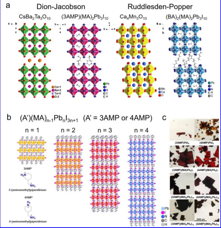
Hybrid organic-inorganic halide perovskites materials with three-dimensional (3D) AMX3 structures enable solar cells with power conversion efficiency (PCE) over 22%.1-7 With impres-sive structural diversity and great potential in optoelectronic ap-plications, two-dimensional (2D) hybrid organic-inorganic hal-ide perovskites are evolving into an important class of high-per-formance semiconductors.8-22 2D halide perovskites, A’
2A n-1MnX3n+1 or A’An-1MnX3n+1, (A’ = 1+ or 2+, A = 1+ cation, M = Pb2+, Sn2+, Ge2+, Cu2+, Cd2+ etc., X = Cl-, Br- and I-), are classi-fied depending on the stacking orientation of the inorganic lay-ers ((100), (110) or (111) with respect to the ideal cubic perov-skite), but also on the number of the inorganic layers (n = 1, 2, 3 etc, in the chemical formula).10, 23 The single-layered 2D per-ovskites (n = 1) which have a general formula of A2MX4 or AMX4 (have been extensively explored and there is a large number of structural types reported to date, differing in the na-ture of the organic spacers and the configuration of the inor-ganic layers.10, 24-25 For the higher number of layers (n ≥ 2), how-ever, there are only few crystallographically characterized ex-amples: (PEA)2(MA)n-1PbnI3n+1 (n = 2, 3)14, 26 (PEA = phenyle-thylammonium, MA = methylammonium), (BA)2(MA) n-1PbnI3n+1 (n = 2 - 5) (BA = butylammonium),27-28 (GA)(MA)nPbnI3n+1 (GA = guanidinium, n = 2 - 3),29 (BA)2(MA)n-1SnnI3n+1 (n = 2 - 3),23, 30 (CH3C6H4CH2NH3)2 (MA)Pb2I7,31 (HO2C(CH2)3NH3)2(MA)Pb2I7,32 (C4H3SCH2NH3)2 (MA)Pb2I7,33 (EA)4Pb3X1034 (X = Cl, Br) (EA = ethylammonium), (BA)(MA)PbBr 35 and
Cs2[C(NH2)3]Pb2Br7.36 The layered structures, historically, can be divided into several categories, based on the nomenclature of oxide perovskites:37 a) Ruddlesden-Popper (RP) phases,27, 38 b) Dion-Jacobson (DJ)39-40 (Figure 1a), the oxide perovskite specific c) Aurivilius (AV) phases41 and the halide perovskite specific d) alternating cation in the interlayer space (ACI) type.29 The differences between these categories are shown in the relative stacking of the layers. The halide perovskites are dominated by the RP archetypes which are characterized by two offset layers per unit cell (Figure 1a). having pairs of interdigi-tated interlayer spacers (1+). The DJ perovskites feature diva-lent (2+) interlayer spacers, requiring only one cation per for-mula unit,42-45 and tend to adopt the RbAlF
4 structure-type.46 Because of this, DJ perovskites have a rich configurational ste-reochemistry with the layers being able to stack in a perfect (0,0 displacement, as reported here) or imperfect (0, ½ or ½, ½ dis-placements) arrangement according to the steric demands of the interlayer cations, as derived from oxide chemistry.47 The oxide DJ perovskites have been studied extensively due to their inter-esting ion-exchange48-49 and intercalation50 properties. In halide perovskites, beyond the single-layer perovskites (n = 1) very little is known regarding the higher n-members in the perovskite hierarchy.
1
2
3
4
5
6
7
8
9
10
11
12
13
14
15
16
17
18
19
20
21
22
23
24
25
26
27
28
29
30
31
32
33
34
35
36
37
38
39
40
41
42
43
44
45
46
47
48
49
50
51
52
53
54
55
56
57
58
Here we report the first examples of hybrid DJ hybrid 2D lead iodide perovskites which consist of thick perovskite slabs (n>1) with layer number (n) ranging from 1 to 4. We describe two new DJ perovskite series based on bivalent (+2) organic cations deriving from a piperidinium (C5NH12) organic back-bone (Figure 1b). The new DJ perovskites are built from 3AMP (3AMP = 3-(aminomethyl)piperidinium) and 4AMP (4AMP = 4-(aminomethyl)piperidinium) cations between the layers (“spacers”) and methylammonium (MA) cations inside the 2D layers (“perovskitizers”) to form (A’) (MA)n-1PbnI3n+1 (A’ = 3AMP or 4AMP, n = 1-4) homologous series.51 With the excep-tion of the n = 1 members, the 3AMP and 4AMP series with a
representative crystal structure sequence shown in Figure 1b. We find that the difference in the position of the-CH2NH3+ group on the piperidine chair (3- and 4- position with respect to the piperidine nitrogen) influence the crystal structure through different hydrogen bonding modes, which is further reflected on the distortion of the inorganic layers. This difference has a ma-jor impact on the optical and electronic properties, which see a narrowing of the bandgap and an enhanced charge transport per-formance for the least distorted structure (3AMP). Density functional theory calculations (DFT)
Figure 1. a, Comparison between Dion-Jacobson phases and Ruddlesden-Popper phases for both oxide and halide perovskite. Crystal struc-ture of CsBa2Ta3O10, Ca4Mn3O10 and (BA)2(MA)2Pb3I10 are adopted from reference 41, 38 and 27. b, General crystal structure of the two
series of DJ perovskite reported here, from n = 1 to 4. Structures of the cation 3AMP and 4AMP are listed in the lower left corner. c, Optical images of the 3AMP and 4AMP crystals. Scale bar on the bottom right applies to all.
1
2
3
4
5
6
7
8
9
10
11
12
13
14
15
16
17
18
19
20
21
22
23
24
25
26
27
28
29
30
31
32
33
34
35
36
37
38
39
40
41
42
43
44
45
46
47
48
49
50
51
52
53
54
55
56
57
Table. 1 Crystal data and structure refinement for A′MAn-1PbnI3n+1 (A’ = 3AMP or 4AMP).
Compound (3AMP)PbI4 (3AMP) (MA)Pb2I7 (3AMP) (MA)2Pb3I10 (3AMP) (MA)3Pb4I13 Empirical
formula C6N2H16PbI4 (C6N2H16)(CH3NH3)Pb2I7 (C6N2H16)(CH3NH3)2Pb3I10 (C6N2H16)(CH3NH3)3Pb4I13
Crystal system Monoclinic
Space group P2 1/c Ia Pa Ia Unit cell dimensions a = 8.6732(6) Å, b = 18.4268(9) Å, c = 20.4522(14) Å, β = 99.306(6) ° a = 8.8581(11) Å, b = 8.8607(4) Å, c = 33.4749(5) Å, β = 90° a = 8.8616(3) Å, b = 8.8624(3) Å, c = 23.0316(7) Å, β = 90° a = 8.8627(18) Å, b = 8.8689(18) Å, c = 58.842(12) Å, β = 90° Volume (Å3) 3225.67(35) 2627.4(3) 1808.79(10) 4625.1(16) Z 8 4 2 4 Density (g/cm3) 3.4224 3.6681 3.8024 3.8645 Indepd. refl. [R 5033 int = 0.1102] 4422 [R int = 0.0202] 8035 [Rint = 0.0361] 5893 [R int = 0.0405] Data / restraints / param. 5033 / 32 / 145 4422 / 17 / 115 8035 / 28 / 163 5893 / 19 / 201 Final R indi-ces [I>2σ(I)] R obs = 0.0869, wR obs = 0.1622 R obs = 0.0323, wR obs = 0.0922 Robs = 0.0395, wRobs = 0.1063 R obs = 0.0901, wR obs = 0.2062 R indices [all data] Rall = 0.1471, wRall = 0.1686 Rall = 0.0365, wRall = 0.0941 Rall = 0.0612, wRall = 0.1296 Rall = 0.1136, wRall = 0.2138 Largest diff.
peak and hole 3.97 and -4.88 e·Å -3
1.44 and -1.23 e·Å-3 2.014 and -1.382 e·Å-3 11.07 and -5.34 e·Å-3 Compound (4AMP)PbI
4 (4AMP) (MA)Pb2I7 (4AMP) (MA)2Pb3I10 (4AMP) (MA)3Pb4I13 Empirical
for-mula
C6N2H16PbI4 (C6N2H16)(CH3NH3)Pb2I7 (C6N2H16)(CH3NH3)2Pb3I10 (C6N2H16)(CH3NH3)3Pb4I13
Crystal system Monoclinic
Space group Pc Ia Pc Ia
Unit cell di-mensions a = 10.4999(13) Å, b = 12.5429(9) Å, c = 12.5289(13) Å, β = 89.984(9)° a = 8.8412(11) Å, b = 8.8436(4) Å, c = 33.6045(5) Å, β = 90° a = 23.1333(7) Å, b = 8.8365(3) Å, c = 8.8354(3) Å, β = 90° a = 8.8587(18) Å, b = 8.8571(18) Å, c = 58.915(12) Å, β = 90° Volume (Å3) 1650.05(43) 2627.5(4) 1806.11(10) 4622.6(16) Z 4 4 2 4 Density (g/cm3) 3.3441 3.6681 3.8081 3.8666 Indepd. refl. 4646 [Rint = 0.1198] 4558 [Rint = 0.028] 7954 [Rint = 0.0291] 8002 [Rint = 0.1339] Data / restraints / param. 4646 / 36 / 141 4558 / 17 / 116 7954 / 18 / 158 8002 / 19 / 202 Final R
indi-ces [I>2σ(I)] wRRobs = 0.0797, obs = 0.1093 Robs = 0.0330, wRobs = 0.0915 Robs = 0.0351, wRobs = 0.0889 Robs = 0.0585, wRobs = 0.0839 R indices [all data] Rall = 0.1618, wR all = 0.1275 Rall = 0.0410, wR all = 0.0949 Rall = 0.0559, wRall = 0.0970 Rall = 0.1700, wRall = 0.1000 Largest diff.
peak and hole 4.48 and -4.31 e·Å 3
1.69 and -1.20 e·Å-3 1.80 and -1.39 e·Å-3 4.23 and -2.94 e·Å-3 R = Σ||Fo|-|Fc|| / Σ|Fo|, wR = {Σ[w(|Fo|2 - |Fc|2)2] / Σ[w(|Fo|4)]}1/2 and w=1/(σ2(I)+0.0004I2)
1
2
3
4
5
6
7
8
9
10
11
12
13
14
15
16
17
18
19
20
21
22
23
24
25
26
27
28
29
30
31
32
33
34
35
36
37
38
39
40
41
42
43
44
45
46
47
48
49
50
51
52
53
54
55
56
57
58
calculations are in good agreement with the observed trends. We further demonstrate the superior optoelectronic properties of these materials on photovoltaic (PV) devices. Owing to the less distorted crystal structure the 3AMP series shows a supe-rior performance (~7% champion efficiency for n = 4) to the 4AMP series (~5% champion efficiency for n = 4). These two series of examples showcase the power of utilizing different
templating organic cations to influence the semiconducting properties of the inorganic part of the perovskites, which broaden the horizons of 2D perovskites for achieving new solar cells and other optoelectronic devices with better characteris-tics.
Results and discussion
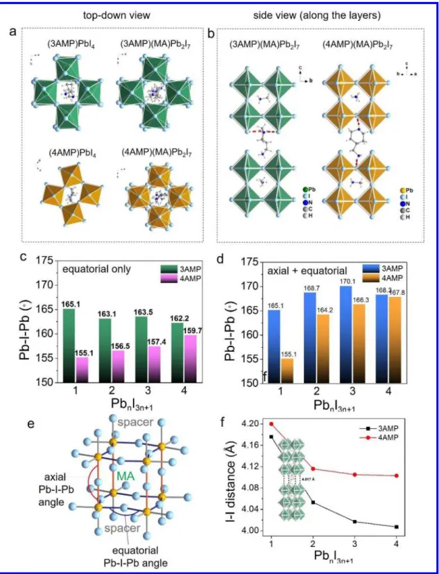
Figure 2. a, Top-view of (3AMP)PbI4, (4AM)PPbI4, (3AMP)(MA)Pb2I7 and (4AMP)(MA)Pb2I7. b, Side-view of (3AMP)(MA)Pb2I7 and
(4AMP)(MA)Pb2I7, hydrogen bonding is marked in red. c, Average equatorial Pb-I-Pb angles for 3AMP and 4AMP series from n = 1 to 4. d, Average axial and equatorial angles for 3AMP and 4AMP. e, Definition of axial and equatorial Pb-I-Pb angles. f, I∙∙∙I distance trend in
3AMP and 4AMP, where the 3AMP series has closer distance.
1
2
3
4
5
6
7
8
9
10
11
12
13
14
15
16
17
18
19
20
21
22
23
24
25
26
27
28
29
30
31
32
33
34
35
36
37
38
39
40
41
42
43
44
45
46
47
48
49
50
51
52
53
54
55
56
57
The structural differences between RP and DJ halide perov-skites are mainly caused by the inter-layer cations (spacers), where RP phases have two sheets of interdigitating cations (1+) while the DJ phases only have one sheet of inter-layer cations (2+) between the inorganic slabs.The influence of the spacers on inorganic slabs is exerted in many levels, depending on the cation size and shape (steric effect), charge (electrostatic attrac-tion) and the position of the functional groups (H-bonding and dispersion forces). This difference between RP and DJ perov-skites is also reflected on the general formula, where RP phase has a general formula of A’2An-1MnX3n+1 and DJ phase has a general formula of A’An-1MnX3n+1 (A’ = inter-layer cation). In hybrid DJ phases, the inter-layer organic cations are 2+, having less degrees of freedom, making the layers closer to each other. In RP phases, the organic cations are 1+, which results in more flexible layer stacking.
The Dion-Jacobson series of layered perovskites, (A’)(MA) n-1PbnI3n+1 (A’ = 3AMP or 4AMP, n = 1- 4), produce uniform, square plate-like crystals, except 3-AMPPbI4, which is an elon-gated plate as seen in Figure 1c. For the 3AMP series, the color of the crystal gets progressively darker from n = 1 (red) to n = 4 (black). The 4AMP has a similar trend, but it starts from lighter colors than the 3AMP for the n = 1 (orange) and n = 2 (red) members. The bulk crystals exhibit good stability in am-bient environment and can be handled without any protection during characterizations.
Both (A’)(MA)n-1PbnI3n+1 series form isostructural analogues for n>1. Detailed crystallographic data and structural refine-ments for all eight compounds reported here are listed in Table 1. They consist of n layers (~6.3 Å is the thickness of one octa-hedron) of corner-sharing [PbI6]4- octahedra with xAMP2+ (x = 3, 4) separating the perovskite slabs and MA+ filling in the per-ovskite voids (Figure 1b). The difference between the two DJ perovskite families is highlighted in Figure 2a and 2b, where specific crystallographic characteristics are stressed. The n = 1 and n = 2 members of each AMP series are selected as repre-sentative examples. For n = 1, the layers stack almost exactly on top of one another from the top-down viewing direction. (3AMP)PbI4 is somewhat mismatched due to an out-of-plane tilting. (4AMP)PbI4 matches perfectly as it displays exclusively large in-plane tilting. The 3AMP and 4AMP behave alike when it comes to n = 2, where the difference only lies in the Pb-I-Pb angle. The trend continues for the higher numbers (n = 3 and 4). Viewing along the inorganic layers (Figure 2b), the hydrogen bonding networks for 3AMP and 4AMP are drastically differ-ent. In (3AMP)(MA)Pb2I7, the 3AMP cation forms weak H-bonds (highlighted in red) with the terminal I-. Bonding with the terminal I- has a small effect on the in-plane Pb-I-Pb angles as the terminal I- does not contribute to the in-plane distortion di-rectly. On the contrary, in (4AMP)(MA)Pb2I7, the H-bonds are formed with the bridging I- anions deeper inside the layers as seen in Figure 2b, which amplify the in-plane distortion.
The differences in hydrogen bonding have an impact on the Pb-I-Pb angles, which are directly related to the optical and electrical these materials (see below). To illustrate this point, we classify the Pb-I-Pb angles into two categories, the axial (along the longest crystallographic axis) and the equatorial (along the inorganic plane) as shown in Figure 2e. In these systems, the axial Pb-I-Pb angles are very close to 180°, as they are much less affected by the inter-action (e.g. hydrogen bonding) with the spacing cations. On the
other hand, the equatorial Pb-I-Pb angles are much more distorted since they are directly exposed to the spacing cations, especially for the case of n = 1 and n = 2. The evolution of the Pb-I-Pb angles is summarized in Figure 2c and 2d, where Figure 2c shows only the averaged equatorial angles and Figure 2d shows the averaged (both axial and equatorial) Pb-I-Pb angles. From Figure 2c, it is clear the gap between the average of the equatorial angles of the 3AMP and 4AMP gradually closes as the layer thickness increases from n = 1 to 4. For 3AMP, the averaged equatorial Pb-I-Pb decreases from 165.1 ̊ to 162.2 ̊ while for 4AMP it increases from 155.1 ̊ to 159.7 ̊. This indicates that the effect of organic cation on the inorganic slabs is gradually diminished as they get thicker (increasing n num-ber). As the axial Pb-I-Pb angles in both series are close to 180 ̊, when they are averaged with the equatorial angles as shown in Fig-ure 2d, the average is increased for both series up to n = 4.
Another interesting structural feature is that the I···I distance
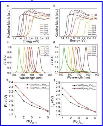
be-tween the inorganic layers is very short. Since the layers lay exactly Figure 3. Optical properties of the 3AMP and 4AMP series.
a,b, Optical absorption spectra of 3AMP and 4AMP series. c,d, Steady-state photoluminescence (PL) spectra of 3AMP
and 4AMP series. e,f, Summary of absorption and PL in en-ergy from n = 1 to 5.
Figure 4. Comparison of the a. optical absorption spectra and
b. PL spectra between (3AMP)(MA)2Pb3I10,
(4AMP)(MA)2Pb3I10, (GA)(MA)3Pb3I10 and
(BA)2(MA)2Pb3I10. 600 650 700 750 0.0 0.2 0.4 0.6 0.8 1.0 3AMP 4AMP GA BA I / a.u. Wavelength (nm) n = 3 1.4 1.6 1.8 2.0 2.2 2.4 3AMP 4AMP GA BA Kubelka-Mu nk (a.u.) Energy (eV) n = 3 a b
1
2
3
4
5
6
7
8
9
10
11
12
13
14
15
16
17
18
19
20
21
22
23
24
25
26
27
28
29
30
31
32
33
34
35
36
37
38
39
40
41
42
43
44
45
46
47
48
49
50
51
52
53
54
55
56
57
58
on top of each other (eclipsed configuration), the I···I distance es-sentially defines the closest interlayer distance. The 3AMP series has generally smaller I···I distance than 4AMP (Figure 2d), while for both series the I···I distance gradually decreases slightly as the layer gets thicker. This is possibly a result of increased stacking fault formation in the perovskite layers as n increases, expressed indirectly in the determined average crystallographic structure. The close I···I interlayer distance (~ 4.0 Å) is one of the shortest among reported 2D lead iodide perovskites and plays a crucial role in affecting the electronic band structure of these materials which will be discussed below.
The optical band gaps of both 3AMP and 4AMP series follow a general trend that has the energy gap (Eg) decreasing as the layer
number (n) increases (Table 2). From n = 1 to n = ∞ (MAPbI3), the
band gap decreases from 2.23 eV to 1.52 eV for the 3AMP series, while for the 4AMP the range is much wider (2.38 eV to 1.52 eV) (Figures 3a, 3b). The spectra of both series show clear excitonic features similarly to other 2D perovskites,13, 18, 28, 51-52 which
be-come less prominent as the n number increases and finally disap-pear for n = ∞. The steady-state photoluminescence (PL) spectra of these materials, shown in Figures 3c, d, exhibit an analogous trend with the band gaps. The 3AMP series demonstrates con-stantly lower PL emission energy than the 4AMP, until n = 5 when they become equal. Though the evolution of the band gap of both series matches the PL trend, from n = 3 and above, the difference between the two series is negligible (Figures 3e, f). The lifetimes of both AMP series (Figure S6) are comparable to the previously
reported 2D layered perovskite PEA (PEA = phenylethylamine) se-ries, for which the lifetimes lie in the 0.1 – 0.2 ns range.53 Overall
the 3AMP series has longer lifetime than the 4AMP (except n = 1), which indicates slower carrier combination, more ideal for the PV devices.
The optical properties of the DJ iodide perovskites are quite dif-ferent from those observed in RP perovskites.51 Relative to the
cor-responding RP perovskites (Figure 4), the emission energy ob-served in PL is characteristically red shifted by ~ 0.1 eV in the case of 3AMP (1.90 eV) and 0.03 eV in the case of 4AMP (1.97 eV) with respect to the BA analogue (2.00 eV), taking n = 3 as the ref-erence example.51 The absorption edges of the compounds
con-taining AMPs (1.70 eV) are also 0.1 eV lower than the BA ana-logue. The recently reported structural type ACI perovskite GAMA3Pb3I10 falls in between the RP and DJ perovskites, with a
Eg of 1.73 eV and PL emission peak at 1.96 eV. 29
The optical properties of these materials correlate very well with their structural characteristics. As discussed above, the Pb-I-Pb an-gles for 3AMP are systematically larger than the 4AMP. The larger Pb-I-Pb bond angles (closer to 180 ̊), the more the Pb s and I p or-bitals overlap.54-56 The strong anti-bonding interaction pushes up
the valence band maximum (VBM), resulting in a reduced band gap. Thus, the systematically narrower band gap observed for 3AMP vs 4AMP can be attributed to the more linear Pb-I-Pb angles (i.e. smaller octahedral tilting (Figure S7))for the former.
Table 2. Optical properties and color of the (A’)(MA)n-1PbnI3n+1 (A’ = 3AMP or 4AMP, n = 1- 4) DJ perovskites.
Compound Eg (eV) PL (eV) Color Compound Eg (eV) PL (eV) Color
n = 1 (3AMP)PbI4 2.23 2.22 red (4AMP)PbI4 2.38 2.33 orange
n = 2 (3AMP)(MA)Pb2I7 2.02 2.00 dark red (4AMP)(MA)Pb2I7 2.17 2.13 red
n = 3 (3AMP)(MA)2Pb3I10 1.92 1.90 black (4AMP)(MA)2Pb3I10 1.99 1.97 black
n = 4 (3AMP)(MA)3Pb4I13 1.87 1.84 black (4AMP)(MA)3Pb4I13 1.89 1.88 black
a b c d
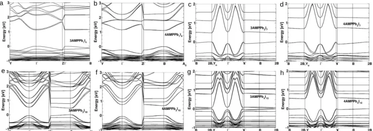
e f g h
Figure 5. a-g, DFT calculations of band structures for the 3AMP and 4AMP series with SOC. The calculated gaps are 1.13 eV for (3AMP)PbI4(at Ґ), 1.14 eV for (4AMP)PbI4 (at B), 0.48 eV for (3AMP)(MA)Pb2I7 (at Yo), 0.70 eV for (4AMP)(MA)Pb2I7 (at Yo), 0.47
eV for (3AMP)(MA)2Pb3I10 (at Z), 0.74 eV for (4AMP)(MA)2Pb3I10 (at Z), 0.07eV for (3AMP)(MA)3Pb4I13 (at Yo), 0.54 eV for
(4AMP)(MA)3Pb4I13 (at Yo)
1
2
3
4
5
6
7
8
9
10
11
12
13
14
15
16
17
18
19
20
21
22
23
24
25
26
27
28
29
30
31
32
33
34
35
36
37
38
39
40
41
42
43
44
45
46
47
48
49
50
51
52
53
54
55
56
57
The results of Density Functional Theory (DFT) electronic struc-ture calculations are shown in Figure 5a-g. The calculated band gap for (3AMP)PbI4 is determined at the Ґ point (1.13 eV) (Figure
5a), whereas the band gap of (4AMP)PbI4 is determined at the BZ
edge (1.14 eV) (Figure 5b). The calculated band gaps for the higher numbers between the 3AMP and 4AMP series have larger differ-ences, where Eg is 0.48 eV for n = 2, 3AMP, and 0.70 eV for n = 2,
4AMP (Figure 5c- d). For n = 3, the band gaps at Z point for 3AMP and 4AMP are 0.47 eV and 0.74 eV, respectively (Figure 5e -f). The calculated gap for 3AMP (n = 4) is very small (0.07 eV), much lower than 0.54 eV for n = 4, 4AMP as seen in Figure 5g -h. The DFT computed band gaps do not include many-body interactions needed to properly assess optical response, which is why calculated values are systematic underestimated without GW corrections.57
The band gaps of 3AMP series DJ are systematically smaller than those computed for 4AMP series as shown in Figure 5h, in agree-ment with experiagree-mental findings. The stacking of perovskite sheets in the DJ structure type, which aligns the perovskite layers, allows for a better interlayer electronic coupling through van der Waals I…I interactions. These I…I contacts participate in anti-bonding in-teractions that further destabilize the VBM (Figure S9), contrib-uting to the reduction of the band gap as compared to RP phases with respect to the same n-value, as discussed above.
Based on the attractive properties of the new 2D DJ perovskites, in a preliminary study we investigated the higher layer numbers (n = 3 and 4) as light absorbers for solar cells. A planar solar cell struc-ture was adopted for device fabrication (Figure 6a), consisting of a fluorine doped tin oxide (FTO) substrate, a poly(3,4-ethylenediox-ythiophene) polystyrene sulfonate (PEDOT:PSS) hole transport layer (HTL), a 2D perovskite light absorber, a C60/BCP electron
transport layer (ETL) and a Ag electrode. The devices were fabri-cated using a modified solvent engineering method (see Methods). The photocurrent density-voltage (J-V) curves of the solar cells us-ing the 2D DJ perovskites are in Figure 6b, (measured usus-ing a re-verse voltage scan). The thickness of the perovskite films was ~250 nm. Among the n = 3 and 4 for 3AMP and 4AMP, (3AMP)(MA)3Pb4I13 achieved the highest power conversion
effi-ciency (PCE) of 7.32% with a short-circuit current density (Jsc) of
10.17 mA∙cm-2, an open-circuit voltage (V
oc) of 1.06 V, and a fill
factor (FF) of 67.60%. This value is significantly higher that the corresponding n = 3 and n = 4 RP perovskites prepared using a regular mesoporous TiO2 device structure.
The remarkable performance of (3AMP)(MA)3Pb4I13 can be
mainly attributed to the reduced band gap and the improved mobil-ity originating from the increased band dispersion (see above). While the device based on (3AMP)(MA)2Pb3I10 has the lowest PCE
of 2.02% with a Jsc of 3.05 mA∙cm-2, a Voc of 0.99 V, and a FF of
66.54%, attributed to the largest band gap and the intense presence of a secondary phase, identified as the n = 2 member (2θ = ~11° and ~16°). (4AMP)(MA)2Pb3I10 and (4AMP)(MA)3Pb4I13 have
PCE below 5%, mainly due to the much lower Jsc relative to the
3AMP. The average photovoltaic parameters of the devices using the various absorbers are summarized in Table S6. The Jsc
inte-grated from the external quantum efficiency (EQE) curves (Figure 6c) of the devices based for (3AMP)(MA)2Pb3I10,
(3AMP)(MA)3Pb4I13, (4AMP)(MA)2Pb3I10 and
(4AMP)(MA)3Pb4I13 are 2.92, 10.16, 5.83, and 7.08 mA∙cm-2,
re-spectively, which are in good agreement with the trend of the Jsc
obtained from the J-V curves. In Figure 6d, powder x-ray diffrac-tion (PXRD) of the (3AMP)(MA)3Pb4I13, (4AMP)(MA)2Pb3I10 and
(4AMP)(MA)3Pb4I13 films show preferred orientation in the
“per-pendicular” direction judging from the strongest hkl (110) and (220) at ~14° and ~28°, which facilitates the carriers to travel through
the layers.8, 13 Further results of the fabrication of higher quality
films and higher efficiency solar cells will be reported in the future. PL emission properties of the films (Figure 6e) are quite different (red shifted) from the bulk materials, which can be attributed to the so-called “edge effect”.52 The edge effect is observed in single
crystals of both 3AMPPbI4 and (3AMP)(MA)2Pb3I10 as seen in
Fig-ure S11. The second PL emission at lower energy were observed when excited the sample through “the edge”, which is parallel to the layers. The results show larger separation of the higher (2.21 eV from bulk) and lower energy emission (1.64 eV edge) of the n = 1 than for n = 3 (1.91 eV and 1.68 eV) for 3AMP. The lower energy emission (1.68 eV) is very close to the emission of the thin film (1.66 eV). This result is similar to the previously reported (BA)2(MA)2Pb3I10 example, where the higher energy emission is
2.00 eV and lower energy emission is 1.70 eV.52 Attempts for
measuring edge states of the other layered number crystals such as n = 2 and 4 were not successful owing to the thin crystal morphol-ogy which has caused handing difficulty.
The absorption edges of the films have the same trend as in the EQE spectra, though multiple slopes appear, indicating the
for-mation of some lower layer numbers (Figure 6f). Even though these 2D DJ perovskite devices are not completely optimized, the initial results show great promise as they compare well with the corre-sponding 2D RP perovskites which lead the 2D perovskite solar cells field.8, 15, 58
Conclusions
We have shown that a new crystal motif based on the DJ class of perovskites forms 2D hybrid lead iodide perovskites. The
Figure 6. Solar cell architecture for the higher layer numbers (n = 3 and 4) of 3AMP and 4AMP.a, Scheme of the adopted inverted
device structure. b, J-V curves of the 2D perovskite solar cell de-vices. c, External quantum efficiency (EQE) spectra. d, PXRD of the thin-films. e, steady-state PL spectra, where the emission peaks: 746 nm, 1.66 eV(3AMPPb3I10), 764 nm, 1.62 eV
(3AMPPb4I13), 752 nm, 1.65 eV (4AMPPb3I10 and 4AMPPb4I13). f, Absorption spectra for the thin-films.
0.0 0.3 0.6 0.9 1.2 0 2 4 6 8 10 12 Current denisty (mA cm -2) Voltage (V) 3AMPPb3 3AMPPb4 4AMPPb3 4AMPPb4 400 600 800 0 20 40 60 EQE (%) Wavelength (nm) 3AMPPb3 3AMPPb4 4AMPPb3 4AMPPb4 FTO PEDOT:PSS 2D perovskite C60 BCP Ag 700 750 800 850 PL (a.u.) Wavelength (nm) 3AMPPb3 3AMPPb4 4AMPPb3 4AMPPb4 10 20 30 40 50 * * * * * * * * ** * * FTO (400) (220) (200) Inten sity (a.u.) 4AMPPb4 4AMPPb3 3AMPPb4 3AMPPb3 2 () (110) * * a b d e f c 400 600 800 0.0 0.2 0.4 0.6 0.8 1.0 Abso rbance (a.u.) Wavelength (nm) 3AMPPb3 3AMPPb4 4AMPPb3 4AMPPb4
1
2
3
4
5
6
7
8
9
10
11
12
13
14
15
16
17
18
19
20
21
22
23
24
25
26
27
28
29
30
31
32
33
34
35
36
37
38
39
40
41
42
43
44
45
46
47
48
49
50
51
52
53
54
55
56
57
58
special spacer cations used 3AMP and 4AMP have strong fluence on the overall properties. Detailed crystallographic in-vestigations on all eight compounds (n = 1 to 4, for 3AMP and 4AMP), have provided the structural insights for understanding the structure-property relationships. In particular, by under-standing the angular distortion (Pb-I-Pb angle) within the sys-tem, we manage to show the subtle difference in the cations causes large differences in the optical properties by affecting the Pb-I-Pb angles, where the 3AMP series has systematically larger angles and smaller band gaps than the 4AMP series. Compared to the most common 2D RP perovskites, namely the BA series, the 3AMP and 4AMP series possess lower band gaps because of a less distorted inorganic framework and closer I···I interlayer distances. Our analysis suggests more superior opto-electronic properties of the 3AMP over the 4AMP series, which as demonstrated in the actual device fabrication, where the pre-liminary result shows the champion device has PCE over 7%. The strong correlation between the materials and their applica-tions’ performance validates the importance of understanding structure-property relationships and discovering new materials in the halide perovskite systems.
Methods
Materials. PbO (99.9%), 3-(aminomethyl)piperidine (AldrichCPR),
4-(aminomethyl)piperidine (96%), hydroiodic acid (57 wt. % in H2O, distilled, stabilized, 99.95%) and hypophosphorous acid
so-lution (50 wt. % in H2O) were purchased from Sigma-Aldrich and
used as received. Methylammonium iodide (>99.5%) was pur-chased from Luminescence Technology Corp. and used as re-ceived.
Synthesis of (3AMP)(MA)n-1PbnI3n+1. For n = 1, an amount of 669
mg (3 mmol) 99.9% PbO powder was dissolved in 6 ml of hy-droiodic acid and 1 ml hypophosphorous acid solution by heating under stirring for 5-10 min at ~130°C until the solution turned to clear bright yellow. 0.5 ml hydroiodic acid was added to 342 mg (3 mmol) 3-(aminomethyl)piperidine (3AMP) in a separate vial under stirring. The protonated 3AMP solution was added into the previ-ous solution under heating and stirring for 5 min. Red plate-like crystals precipitate during slow cooling to room temperature. Yield 963 mg (38.6% based on total Pb content). For n = 2, an amount of 669 mg (3 mmol) 99.9% PbO powder was dissolved in 6 ml of hydroiodic acid and 1 ml hypophosphorous acid solution by heat-ing under stirrheat-ing for 5-10 min at 130°C until the solution turned to clear bright yellow. 318 mg (2 mmol) of methylammonium iodide (MAI) was added directly to the above solution under heating. 0.5 ml hydroiodic acid was added to 57 mg (0.5 mmol) 3AMP in a separate vial under stirring. The protonated 3AMP solution was added into the previous solution under heating and stirring for 5 min. Dark red plate-like crystals precipitated (Figure 1c) during slow cooling to room temperature. Yield 487 mg (22.4% based on total Pb content). For the synthesis of higher numbers, they follow the same route except the ratio were change to 37.6 mg (0.33 mmol) 3AMP, 477 mg (3 mmol) MAI, 669 mg (3 mmol) PbO for n = 3, yield 252 mg (12.2% based on total Pb content) and 34.2 mg (0.3 mmol) 3AMP, 636 mg (4 mmol) MAI, 892 mg (4 mmol) PbO for
n = 4, yield 301 mg (11.2% based on total Pb content).
Synthesis of (4AMP)(MA)n-1PbnI3n+1. Similar synthetic
proce-dures were used to synthesize the 4AMP series. However, the amount of 4AMP was reduced as the 4AMP series precipitate faster than the 3AMP. The experimental ratios (4AMP: MAI: PbO) (in mmol) of the 4AMP are 3:0:3 for n = 1, 0.5:2:3 for n = 2, 0.33:3:3 for n = 3 and 0.27:4:4 for n = 4. Yield 1155 mg (46.3%), 684 mg
(31.5%), 531 mg (25.6%) and 477 mg (17.7% based on total Pb content), respectively.
Powder X-ray Diffraction. PXRD analysis was performed using a
Rigaku Miniflex600 powder X-ray diffractometer (Cu Kα graphite, λ = 1.5406 Å) operating at 40 kV/15 mA with a Kβ foil filter.
Single Crystal X-ray Diffraction. Full sphere data were collected
after screening for a few frames using either a STOE IPDS 2 or IPDS 2T diffractometer with graphite-monochromatized Mo Kα radiation (λ = 0.71073 Å) (50 kV/40 mA) under N2 at 293 K
(3AMPPbI4, 4AMPPbI4 and (3AMP)(MA)3Pb4I13). The collected
data was integrated and applied with numerical absorption correc-tions using the STOE X-AREA programs. The rest of the com-pounds were collected using a Bruker Molly instrument with MoKα IμS microfocus source (λ = 0.71073 Å) with MX Optics at 250 K. The collected data was integrated and applied with numeri-cal absorption corrections using the APEX3 software. Crystal structures were solved by charge flipping and refined by full-matrix least squares on F2 with the Jana2006 package.
Optical Absorption Spectroscopy. Optical diffuse reflectance
measurements were performed using a Shimadzu 3600 UV-VIS-NIR spectrometer operating in the 200 – 1000 nm region using BaSO4 as the reference of 100% reflectance. The band gap of the
material was estimated by converting reflectance to absorption ac-cording to the Kubelka–Munk equation: α/S = (1–R)2(2R)−1,
where R is the reflectance and α and S are the absorption and scat-tering coefficients, respectively.
Steady State and Time-resolved Photoluminescence. Steady-state PL spectra were collected using HORIBA LabRAM HR Evolution Confocal RAMAN microscope. 473 nm laser (0.1% power) was used to excite all samples at 50× magnification. Time-resolved photoluminescence (TRPL) spectra were acquired using HORIBA Fluorolog-3 equipped with a 450-W xenon lamp and a TCSPC module (diode laser excitation at λ = 375 nm) and an integrating sphere (Horiba Quanta–φ) for absolute photoluminescence quan-tum yield determination. The spectra were corrected for the monochromator wavelength dependence and photomultiplier response functions provided by the manufacturer.
Electronic Structure Calculations. First-principles calculations are
based on density functional theory (DFT) as implemented in the VASP package.59-61 All calculations are carried out on the
experi-mentally determined crystal structures. We used the GGA func-tional in the PBE form, the projector augmented wave (PAW) method62-63 with the PAW data set supplied in the VASP package
with the following valence orbitals: Pb [5d106s26p2], I [5s25p5], N
[2s22p3], H [1s1] and C [2s22p2]. In addition, the wavefunctions are
expanded using a plane-wave basis set with an energy cut-off of 500 eV. Spin-orbit coupling is systematically taken into account. For band structures, the reciprocal space integration is performed over a 4×4×1 Monkhorst-Pack grid for compounds with n=1 and n=3, and over a 4x4x4 grid for compounds with n=2 and n=4 in their primitive cells.64-65
Device fabrications. FTO glass substrates were coated with
PEDOT:PSS by spin-coating at 4000 rpm for 30s, and then an-nealed at 150 °C for 30 min in air. The 2D perovskite precursors with a molar concentration of 0.6 M were prepared by dissolving the 2D perovskite crystal powders in a mixed solvent of DMF and DMSO with a volume ratio of 4:1. After the crystal powders dis-solved, adding 0.8 vol% HI into the perovskite precursors. Then the precursors were coated on the substrates with a spin rate of 4000 rpm for 60s in a N2-filled glove box. During the spin-coating, 0.7 mL diethyl ether was dropped on the rotating substrates at 20 s.
1
2
3
4
5
6
7
8
9
10
11
12
13
14
15
16
17
18
19
20
21
22
23
24
25
26
27
28
29
30
31
32
33
34
35
36
37
38
39
40
41
42
43
44
45
46
47
48
49
50
51
52
53
54
55
56
57
After spin-coating, the films were annealed at 100 °C for 10 min in the glove box. To complete the devices, C60 (20 nm)/BCP (5 nm)/Ag (100 nm) were sequentially thermally evaporated on top of the perovskites. The active area of the solar cells was 0.09 cm2. Characterizations. J-V curves were measured by a Keithley model
2400 instrument under AM1.5G simulated irradiation with a stand-ard solar simulator (Abet Technologies). The light intensity of the solar simulator was calibrated by a National Renewable Energy La-boratory-certified monocrystalline silicon solar cell. EQE curves were measured by an Oriel model QE-PV-SI instrument equipped with a National Institute of Standards and Technology-certified Si diode.
ASSOCIATED CONTENT
Additional crystallographic details (CIF), thermal analysis (DSC, TGA and DTA), calculation and device data (PDF). This material is available free of charge via the Internet at http://pubs.acs.org.
*Email: [email protected] *[email protected]
This work was supported by the Department of Energy, Office of Science, Basic Energy Sciences, under Grant SC0012541 (synthesis and structural characterization of materials MGK). The device assembly and PL lifetime measurements were sup-ported by the ANSER Center, an Energy Frontier Research Center funded by the U.S. Department of Energy, Office of Sci-ence, and Office of Basic Energy Sciences under Award DE-SC0001059 (WK, MRW). The work at FOTON was performed using HPC resources from GENCI-TGCC/CINES (Grant 2017- 096724). Y.W. thanks the Fulbright Scholars Program for a Graduate Research Fellowship and gratefully acknowledges support of a Ryan Fellowship from the NU International Insti-tute for Nanotechnology (IIN). This work made use of the IMSERC at Northwestern University, which has received sup-port from the Soft and Hybrid Nanotechnology Experimental (SHyNE) Resource (NSF ECCS-1542205); the State of Illinois and International Institute for Nanotechnology (IIN).
1. Kojima, A.; Teshima, K.; Shirai, Y.; Miyasaka, T., J. Am.
Chem. Soc. 2009, 131, 6050-6051.
2. Yang, W. S.; Park, B.-W.; Jung, E. H.; Jeon, N. J.; Kim, Y. C.; Lee, D. U.; Shin, S. S.; Seo, J.; Kim, E. K.; Noh, J. H.; Seok, S. I., Science 2017, 356, 1376-1379.
3. Jeon, N. J.; Noh, J. H.; Kim, Y. C.; Yang, W. S.; Ryu, S.; Seok, S. I., Nat. Mater. 2014, 13, 897-903.
4. Mei, A.; Li, X.; Liu, L.; Ku, Z.; Liu, T.; Rong, Y.; Xu, M.; Hu, M.; Chen, J.; Yang, Y.; Grätzel, M.; Han, H., Science 2014,
345, 295-298.
5. Lee, M. M.; Teuscher, J.; Miyasaka, T.; Murakami, T. N.; Snaith, H. J., Science 2012, 338, 643-647.
6. Green, M. A.; Ho-Baillie, A.; Snaith, H. J., Nat. Photon.
2014, 8, 506-514.
7. Li, X.; Ibrahim Dar, M.; Yi, C.; Luo, J.; Tschumi, M.; Zakeeruddin, S. M.; Nazeeruddin, M. K.; Han, H.; Grätzel, M., Nat.
Chem. 2015, 7, 703-711.
8. Tsai, H.; Nie, W.; Blancon, J.-C.; Stoumpos, C. C.; Asadpour, R.; Harutyunyan, B.; Neukirch, A. J.; Verduzco, R.; Crochet, J. J.; Tretiak, S.; Pedesseau, L.; Even, J.; Alam, M. A.; Gupta, G.; Lou, J.; Ajayan, P. M.; Bedzyk, M. J.; Kanatzidis, M. G.; Mohite, A. D., Nature 2016, 536, 312-316.
9. Yuan, M.; Quan, L. N.; Comin, R.; Walters, G.; Sabatini, R.; Voznyy, O.; Hoogland, S.; Zhao, Y.; Beauregard, E. M.; Kanjanaboos, P.; Lu, Z.; Kim, D. H.; Sargent, E. H., Nat.
Nanotechnol. 2016, 11, 872-877.
10. Saparov, B.; Mitzi, D. B., Chem. Rev. 2016, 116, 4558-4596.
11. Stoumpos, C. C.; Kanatzidis, M. G., Acc. Chem. Res.
2015, 48, 2791-802.
12. Pedesseau, L.; Sapori, D.; Traore, B.; Robles, R.; Fang, H.-H.; Loi, M. A.; Tsai, H.; Nie, W.; Blancon, J.-C.; Neukirch, A.; Tretiak, S.; Mohite, A. D.; Katan, C.; Even, J.; Kepenekian, M.,
ACS Nano 2016, 10, 9776-9786.
13. Cao, D. H.; Stoumpos, C. C.; Farha, O. K.; Hupp, J. T.; Kanatzidis, M. G., J. Am. Chem. Soc. 2015, 137, 7843-50. 14. Smith, I. C.; Hoke, E. T.; Solis-Ibarra, D.; McGehee, M. D.; Karunadasa, H. I., Angew. Chem. Int. Ed. 2014, 53, 11232-11235.
15. Quan, L. N.; Yuan, M.; Comin, R.; Voznyy, O.; Beauregard, E. M.; Hoogland, S.; Buin, A.; Kirmani, A. R.; Zhao, K.; Amassian, A.; Kim, D. H.; Sargent, E. H., J. Am. Chem. Soc.
2016, 138, 2649–2655.
16. Liao, Y.; Liu, H.; Zhou, W.; Yang, D.; Shang, Y.; Shi, Z.; Li, B.; Jiang, X.; Zhang, L.; Quan, L. N.; Quintero-Bermudez, R.; Sutherland, B. R.; Mi, Q.; Sargent, E. H.; Ning, Z., J. Am. Chem.
Soc. 2017, 139, 6693-6699.
17. Mao, L.; Tsai, H.; Nie, W.; Ma, L.; Im, J.; Stoumpos, C. C.; Malliakas, C. D.; Hao, F.; Wasielewski, M. R.; Mohite, A. D.; Kanatzidis, M. G., Chem. Mater. 2016, 28, 7781-7792.
18. Dohner, E. R.; Jaffe, A.; Bradshaw, L. R.; Karunadasa, H. I., J. Am. Chem. Soc. 2014, 136, 13154-13157.
19. Mao, L.; Wu, Y.; Stoumpos, C. C.; Wasielewski, M. R.; Kanatzidis, M. G., J. Am. Chem. Soc. 2017, 139, 5210–5215. 20. Congreve, D. N.; Weidman, M. C.; Seitz, M.; Paritmongkol, W.; Dahod, N. S.; Tisdale, W. A., ACS Photonics
2017, 4, 476-481.
21. Lanzetta, L.; Marin-Beloqui, J. M.; Sanchez-Molina, I.; Ding, D.; Haque, S. A., ACS Energy Lett. 2017, 2, 1662-1668. 22. Tsai, H.; Nie, W.; Blancon, J. C.; Stoumpos, C. C.; Soe, C. M. M.; Yoo, J.; Crochet, J.; Tretiak, S.; Even, J.; Sadhanala, A.,
Adv. Mater. 2018, 30, 1704217.
23. Stoumpos, C. C.; Mao, L.; Malliakas, C. D.; Kanatzidis, M. G., Inorg. Chem. 2017, 56, 56-73.
24. Du, K.-z.; Tu, Q.; Zhang, X.; Han, Q.; Liu, J.; Zauscher, S.; Mitzi, D. B., Inorg. Chem. 2017, 56, 9291-9302.
25. Hautzinger, M. P.; Dai, J.; Ji, Y.; Fu, Y.; Chen, J.; Guzei, I. A.; Wright, J. C.; Li, Y.; Jin, S., Inorg. Chem. 2017, 56, 14991-14998.
26. Calabrese, J.; Jones, N. L.; Harlow, R. L.; Herron, N.; Thorn, D. L.; Wang, Y., J. Am. Chem. Soc. 1991, 113, 2328-2330. 27. Stoumpos, C. C.; Cao, D. H.; Clark, D. J.; Young, J.; Rondinelli, J. M.; Jang, J. I.; Hupp, J. T.; Kanatzidis, M. G., Chem.
Mater. 2016, 28, 2852-2867.
28. Stoumpos, C. C.; Soe, C. M. M.; Tsai, H.; Nie, W.; Blancon, J.-C.; Cao, D. H.; Liu, F.; Traoré, B.; Katan, C.; Even, J.; Mohite, A. D.; Kanatzidis, M. G., Chem 2017, 2, 427-440. 29. Soe, C. M. M.; Stoumpos, C. C.; Kepenekian, M.; Traoré, B.; Tsai, H.; Nie, W.; Wang, B.; Katan, C.; Seshadri, R.; Mohite, A. D.; Even, J.; Marks, T. J.; Kanatzidis, M. G., J. Am. Chem. Soc.
2017, 139, 16297-16309.
30. Mitzi, D. B.; Feild, C. A.; Harrison, W. T. A.; Guloy, A. M., Nature 1994, 369, 467-469.
1
2
3
4
5
6
7
8
9
10
11
12
13
14
15
16
17
18
19
20
21
22
23
24
25
26
27
28
29
30
31
32
33
34
35
36
37
38
39
40
41
42
43
44
45
46
47
48
49
50
51
52
53
54
55
56
57
58
31. Papavassiliou, G. C.; Mousdis, G. A.; Raptopoulou, C.; Terzis, A., Z. Naturforsch. B Chem. Sci. 2000, 55, 536-540. 32. Mercier, N., CrystEngComm 2005, 7, 429-432.
33. Zhu, X.-H.; Mercier, N.; Riou, A.; Blanchard, P.; Frère, P., Chem. Commun. 2002, 2160-2161.
34. Mao, L.; Wu, Y.; Stoumpos, C. C.; Traore, B.; Katan, C.; Even, J.; Wasielewski, M. R.; Kanatzidis, M. G., J. Am. Chem. Soc.
2017, 139, 11956-11963.
35. Luo, J.; Li, L.; Sun, Z.; Wang, P.; Hu, W.; Wang, S.; Ji, C.; Hong, M., Angew. Chem. Int. Ed. 2017, 129, 12318–12322. 36. Nazarenko, O.; Kotyrba, M. R.; Wörle, M.; Cuervo-Reyes, E.; Yakunin, S.; Kovalenko, M. V., Inorg. Chem. 2017, 56, 11552-11564.
37. Schaak, R. E.; Mallouk, T. E., Chem. Mater. 2002, 14, 1455-1471.
38. Battle, P. D.; Green, M. A.; Lago, J.; Millburn, J. E.; Rosseinsky, M. J.; Vente, J. F., Chem. Mater. 1998, 10, 658-664. 39. Dion, M.; Ganne, M.; Tournoux, M., Mater. Res. Bull.
1981, 16, 1429-1435.
40. Hojamberdiev, M.; Bekheet, M. F.; Zahedi, E.; Wagata, H.; Kamei, Y.; Yubuta, K.; Gurlo, A.; Matsushita, N.; Domen, K.; Teshima, K., Cryst. Growth Des. 2016, 16, 2302-2308.
41. Kendall, K. R.; Navas, C.; Thomas, J. K.; zur Loye, H.-C., Chem. Mater. 1996, 8, 642-649.
42. Mousdis, G. A.; Papavassiliou, G. C.; Raptopoulou, C.; Terzis, A., J. Mater. Chem. 2000, 10, 515-518.
43. Rayner, M. K.; Billing, D. G., Acta Cryst. E 2010, 66, m660-m660.
44. Tang, Z.; Guan, J.; Guloy, A. M., J. Mater. Chem. 2001,
11, 479-482.
45. Lemmerer, A.; Billing, D. G., CrystEngComm. 2012, 14, 1954-1966.
46. Bulou, A.; Nouet, J., J. Phys. C Solid State Phys. 1982,
15, 183.
47. Tilley, R. J., Perovskites: Structure-Property Relationships. John Wiley & Sons: 2016; p 123-155.
48. Jacobson, A. J.; Lewandowski, J. T.; Johnson, J. W.,
Mater. Res. Bull. 1990, 25, 679-686.
49. Gopalakrishnan, J.; Bhat, V., Inorg. Chem. 1987, 26, 4299-4301.
50. Jacobson, A. J.; Johnson, J. W.; Lewandowski, J. T.,
Inorg. Chem. 1985, 24, 3727-3729.
51. Stoumpos, C. C.; Cao, D. H.; Clark, D. J.; Young, J.; Rondinelli, J. M.; Jang, J. I.; Hupp, J. T.; Kanatzidis, M. G., Chem.
Mater. 2016, 28, 2852-2867.
52. Blancon, J.-C.; Tsai, H.; Nie, W.; Stoumpos, C. C.; Pedesseau, L.; Katan, C.; Kepenekian, M.; Soe, C. M. M.; Appavoo, K.; Sfeir, M. Y.; Tretiak, S.; Ajayan, P. M.; Kanatzidis, M. G.; Even, J.; Crochet, J. J.; Mohite, A. D., Science 2017, 355, 1288-1292.
53. Peng, W.; Yin, J.; Ho, K.-T.; Ouellette, O.; De Bastiani, M.; Murali, B.; El Tall, O.; Shen, C.; Miao, X.; Pan, J., Nano lett.
2017, 17, 4759-4767.
54. Knutson, J. L.; Martin, J. D.; Mitzi, D. B., Inorg. Chem.
2005, 44, 4699-4705.
55. Katan, C.; Pedesseau, L.; Kepenekian, M.; Rolland, A.; Even, J., J. Mater. Chem. A 2015, 3, 9232-9240.
56. Liu, G.; Kong, L.; Guo, P.; Stoumpos, C. C.; Hu, Q.; Liu, Z.; Cai, Z.; Gosztola, D. J.; Mao, H.-k.; Kanatzidis, M. G.; Schaller, R. D., ACS Energy Lett. 2017, 2518-2524.
57. Even, J.; Pedesseau, L.; Dupertuis, M.-A.; Jancu, J.-M.; Katan, C., Phys. Rev. B 2012, 86, 205301.
58. Zhou, N.; Shen, Y.; Li, L.; Tan, S.; Liu, N.; Zheng, G.; Chen, Q.; Zhou, H., J. Am. Chem. Soc. 2017, 140, 459-465. 59. Kresse, G.; Furthmüller, J., Phys. Rev. B 1996, 54, 11169. 60. Kresse, G.; Furthmüller, J., Comput. Mater. Sci. 1996, 6, 15-50.
61. Shishkin, M.; Kresse, G., Phys. Rev. B 2006, 74, 035101. 62. Blöchl, P. E., Phys. Rev. B 1994, 50, 17953.
63. Kresse, G.; Joubert, D., Phys. Rev. B 1999, 59, 1758. 64. Monkhorst, H. J.; Pack, J. D., Phys. Rev. B 1976, 13, 5188.
65. Pack, J. D.; Monkhorst, H. J., Phys. Rev. B 1977, 16, 1748.