HAL Id: pastel-00001909
https://pastel.archives-ouvertes.fr/pastel-00001909
Submitted on 12 Dec 2011
HAL is a multi-disciplinary open access
archive for the deposit and dissemination of sci-entific research documents, whether they are pub-lished or not. The documents may come from teaching and research institutions in France or abroad, or from public or private research centers.
L’archive ouverte pluridisciplinaire HAL, est destinée au dépôt et à la diffusion de documents scientifiques de niveau recherche, publiés ou non, émanant des établissements d’enseignement et de recherche français ou étrangers, des laboratoires publics ou privés.
Physico-Chimie des plasmas de silane pour la formation
de nacocristaux de silicium a tempétature ambiante :
application à des dispositifs.
Veinardi Suendo
To cite this version:
Veinardi Suendo. Physico-Chimie des plasmas de silane pour la formation de nacocristaux de silicium a tempétature ambiante : application à des dispositifs.. Physique [physics]. Ecole Polytechnique X, 2005. Français. �pastel-00001909�
ECOLE POLYTECHNIQUE
Thèse présentée pour obtenir le grade de
DOCTEUR DE L’ECOLE POLYTECHNIQUE
Spécialité : Science des Matériaux
Par
Veinardi Suendo
Sujet
Low temperature plasma synthesis of silicon
nanocrystals for photonic applications
Soutenue le 25 novembre 2005 devant le jury composé de:
I.
Solomon
Président
L.
Boufendi
Rapporteur
A.
Halimaoui
Rapporteur
P. Roca i Cabarrocas
Directeur de thèse
A.
Gicquel
Examinateur
V.
Paillard
Examinateur
Laboratoire de Physique des Interfaces et des Couches Minces
UMR 7647 du CNRS, Ecole Polytechnique
Remerciements
Ce travail de thèse, financé par la direction des relations extérieurs de l’Ecole Polytechnique (DRE) puis par le Laboratoire de Physique des Interface et des Couches Minces (PICM) de l’Ecole Polytechnique a été effectué au PICM de novembre 2001 à novembre 2005. Pendant ces 4 années, j’ai eu la chance de profiter de l’atmosphère chaleureuse et de haut niveau scientifique dans ce laboratoire. Comme tout travail expérimental, cette thèse est bien sur le résultat d’un travail d’équipe. Je tiens donc à remercier collectivement tous les membres du laboratoire.
Je remercie tout particulièrement mon directeur de thèse Monsieur Pere Roca i Cabarrocas, Directeur de Recherches au CNRS, qui a suivi attentivement la progression de ce travail avec beaucoup des discussions constructives et courageuses.
Je dois remercier Monsieur Roland Sénéor et Madame Cynthia Radiman qui ont commencé la collaboration entre l’Ecole Polytechnique et l’Institut Teknologi Bandung en Indonésie où j’ai eu l’occasion de recevoir une bourse pour continuer mes études dans le cadre du programme doctoral à l’Ecole Polytechnique. Je dois remercier également Monsieur Bernard Drévillon directeur du laboratoire PICM qui m’a introduit à mon directeur de thèse et m’a permis de travailler dans ce laboratoire.
J’exprime toute ma gratitude à Monsieur Ionel Solomon, Directeur de Recherches émérite au CNRS du Laboratoire de Physique de la Matière Condensée à l’Ecole Polytechnique de l’honneur qu’il m’a fait de présider le jury de ma thèse. C’etait toujours un grand plaisir de discuter de science avec lui. J’ai appris beaucoup de lui, en particulièr : « comment faire la physique bon marché ».
Je remercie très vivement Monsieur Laifa Boufendi, Professeur à l’Université d’Orléans qui m’a encouragé pendant ma thèse avec beaucoup d’aides expérimentales, des discussions et aussi pour avoir accepté d’être rapporteur de ce travail.
Je remercie Monsieur Aomar Halimaoui de ST Microélectronique qui a bien voulu s’intéresser à ce travail pour avoir accepté d’être rapporteur de ma thèse.
Je remercie Monsieur Vincent Paillard, Professeur à l’Université de Toulouse qui a bien voulu s’intéresser à ce travail pour des mesures Raman et des discussions, et aussi pour avoir accepté d’être une partie de mon jury de thèse.
Je remercie Madame Alix Gicquel, Professeur à l’Université Paris 13 et Directrice Scientifique au INRETS qui a bien voulu faire partie de mon jury de thèse.
Je remercie Monsieur Ganjar Kurnia et toutes les membres de l’ambassade d’Indonésie en France pour leur aide et leurs encouragements.
Mes remerciements vont à Gilles Patriarche, Carlos Barthou, Andriy V. Kharchenko, Jacques Jolly, Gérard Jaskierowicz, Isabelle Sagnes, Georges Adamopoulos, Satyendra Kumar, Andrei Kosarev, Sarah Lebib, Christian Godet, Jean-Eric Bourrée, Pavel Bulkin, Dmitri Daineka, Shunri Oda, et Holger Vach pour leur aide, le partage de leurs connaissances et des discussions pendant la thèse.
Je remercie Debajyoti Das, Kim Geun-Bom, Anna Fontcuberta i Morral, Yves Poissant, Sandesh Jadkar, Tatiana Novikova, Yvan Bonnassieux, Marc Chatelet, Alexei Abramov, Cyril Jadaud, Gary-Kitchner Rose, Dominique Conne, Dominique Clément, Frédéric Liège, Costel Cojocaru, Jean-Luc Moncel, Didier Pribat, Enric Garcia Caurel, Céline Bernon, Razvigor Ossikovski, Chantal Geneste, Josiane Mabred, Marie-Jo Surmont, Laurence Corbel, et Chisato Niikura pour leur aide et leur amitié pendant quatre années au PICM.
Je remercie mes camarades, thésards, postdocs et stagiaires qui ont partagé les joies d’un tel travail: Fatiha Kail, Jérôme Damon-Lacoste, Muriel Matheron, Billel Kalache, Samir Kasouit, Nihed Chaâbane, Svetoslav Tchakarov, Takashi Katsuno, Marie-Estelle Gueunier-Farret, Kim Doh-Hyung, Quentin Brulin, Nguyen Tran-Thuat, Bui Van-Diep, Nguyen Quang, Dao Thien-Hai, Samira Fellah, Yassine Djeridane, Daniel Soujon, Julie Fargin, Matthieu Thomas, Marie Jouanny, Maxime Mikikian, Marjorie Cavarroc, Pae C. Wu, Rao Rui, Razvan Negru, Nihan Kosku, Céline Baron.
Je remercie ma famille et aussi des amis : Wim Effendi K. S., Tjie Soei Lan, Sparisoma Viridi, Missionnaire Amir, Yohanes Handoyo, Oei Ho Tin, Mauw Wen Liang, Hartoto Halim, Nyi Boen, Andy Surya Rikin, Andy Santoso, Ng Suk Fung, Alwen F. Tiu, Bowie Brotosumpeno, Edy Wijaya, Jeffry Christiandy, Alfred Iskandar, Rofikohrokhim, Pascaline Truc, Leandro Jose Raniero, Shinji et Sayoko Kimura, Bungo Kubota, Akihiko Tanioka, Mie Minagawa, Toshihisa Osaki, Ikuyoshi Tomita, Hidetoshi Matsumoto, Eriko Suzuki, Mariko Kinoshita, Damien Farret, Petr Fojtik, Pavla, Fredy, Diene, Javier, Simona et Luo Wei pour leur amitié, leurs prières, et leurs encouragements pendant mon séjour en France.
Table of contents
1. Introduction ………... 1
References ………... 6
2. Experimental ………. 9
2.1. Plasma Enhanced Chemical Vapor Deposition (PECVD) ………... 9
2.2. Optical Emission Spectroscopy (OES) ……….. 14
2.3. Plasma Impedance Analysis ……….. 17
2.4. Phase Modulated UV-Visible Spectroscopic Ellipsometry (SE) ……….. 19
2.5. Raman Spectroscopy ………. 25
2.6. Infrared Spectroscopy ……… 27
2.7. Photoluminescence (PL) Spectroscopy ………. 30
2.8. Electroluminescence Measurements ………. 37
2.9. High Resolution Transmission Electron Microscopy (HRTEM) ………. 38
2.10. X-ray Energy Dispersive Spectroscopy (XEDS) ……… 39
2.11. Dark Conductivity Measurements ………... 41
2.12. J-V Characteristic Measurements ……… 42
References ………. 42
3. Deposition of hydrogenated polymorphous silicon ……….………. 45
3.1. Introduction ………..………….. 45
3.2. The effects of RF excitation frequency ……….. 48
3.3. Effects of dopants on the dynamics of powder formation and film properties …….. 52
3.4. Photonic applications ………...……….. 57
4. Deposition of hydrogenated polymorphous silicon carbon alloys ……….. 63
4.1. Introduction ……… 63
4.2. Deposition hydrogenated polymorphous silicon carbon alloys ………. 66
4.3. Monitoring particle growth by the evolution of plasma electrical parameters …….. 73
4.4. study of reactive species by optical emission spectroscopy ……….…….… 80
4.5. Chemical analysis of thin films ………. 93
4.6. Structure and morphology of thin films ……… 97
4.7. Summary and conclusions ………... 108
References ………... 109
5. Optoelectronic properties of pm-Si1-xCx:H A material for photonic applications ……….. 113
5.1. Introduction ………. 113
5.2. Optical properties of polymorphous silicon carbon alloys ………. 114
5.3. Photoluminescence of polymorphous silicon carbon alloys ………... 132
5.4. Surface effects ………. 155
5.5. Summary and conclusions ………... 164
References ……….. 167
6. Conclusions and Perspectives ………. 171
Appendix A: Introduction to silicon nanocrystal based photonics …………..……….. 175
Appendix B: From material to devices ………. 193
Chapter 1
Introduction
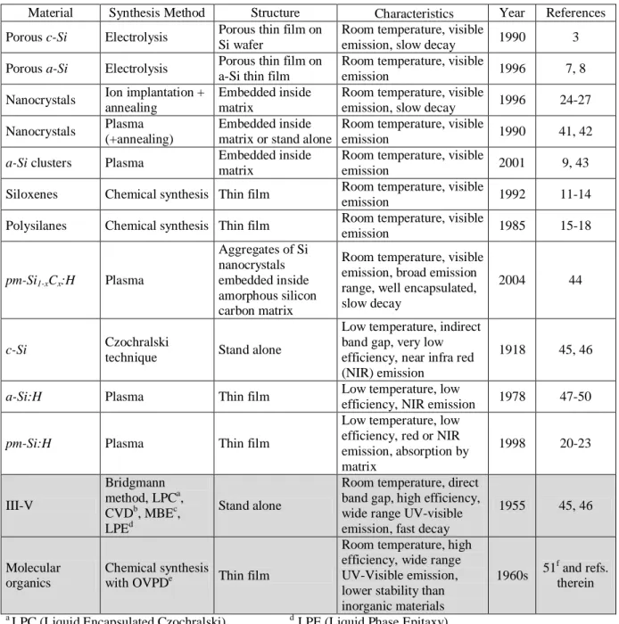
Information technology has grown rapidly in the last few decades and is becoming one of the basic needs of humankind. As this technology grows, the demand for new materials to develop it also increases. So far, silicon is the main semiconductor material for electronic applications, while III-V semiconductors are the main materials for photonic applications. We readily find silicon integrated circuits (ICs) around us: in our cellular phones, personal computers, cars, home appliances, etc. For the further development of this technology, a material compatible with silicon microelectronics and suitable optoelectronic properties would play an important role. In particular, research should focus on a material which could be used for the next generation of photon emitters and could be integrated directly into an IC. Indeed, it is well-known that due to its indirect band-gap structure, bulk silicon is an extremely inefficient photon emitter. Therefore, scientists have turned their interests to other more complex and expensive semiconductor materials such as GaAs (gallium arsenide), InP (indium phosphide), GaP (gallium phosphide), etc. Even though these materials have allowed the realization of laser diodes, they cannot be easily associated with silicon integrated circuits. They are incompatible because the two materials have different crystal lattice constants, a so-called lattice mismatch. Another type of materials, which also give good luminescent efficiency are organic materials. In this case, one does not encounter the lattice mismatch problem due to their amorphous structure, but their processing into devices is not always compatible with microelectronics industry standards. Moreover, the stability of these materials is quite low compared to their inorganic counterparts. As a short summary, silicon related light emitting materials and their references are listed in Table 1.1.
To simplify these problems and to develop optoelectronic devices, it would be better if silicon itself could emit light. The discovery of luminescence from porous silicon and nanosized silicon structures gave new hope for the development of an all-silicon laser [1, 2]. Hitherto, many approaches have been carried out to produce these nanostructures such as the synthesis of porous silicon, silicon nanocrystals, and silicon nanoclusters using various methods [3-5]. The idea behind these approaches is quantum confinement and the breakdown of the k-conservation rule in the silicon nanostructures, which facilitates the radiative recombination in these materials [6]. Moreover, the discovery of luminescence from various
silicon related materials such as porous amorphous silicon [7, 8], amorphous silicon nanoclusters [9,10], siloxenes [11-14], and polysilanes [15-18] has given a strong encouragement to research in this field.
Polymorphous silicon
Another important issue in this research is the synthesis of the material itself, where the growth method is preferably simple, scaleable, and compatible with typical microelectronics industry processes. The formation of silicon particles in the plasma phase using PECVD (plasma enhanced chemical vapor deposition) appears to be an interesting alternative to optimize PL and device fabrication. The discovery of a new material in the field of solar cells and large area electronics, namely hydrogenated polymorphous silicon (pm-Si:H), which consists of silicon nanocrystals (formed in the plasma phase) embedded in an amorphous matrix [19], has given a new perspective on the formation of silicon nanostructures using the PECVD technique.
Hydrogenated polymorphous silicon (pm-Si:H) has a unique structure (more ordered amorphous matrix, embedded nanocrystals, etc.) [20], good electronic properties (low defect density, stability against light soaking, etc.) and a simple preparation method (standard RF-PECVD at low temperature), which makes it a good alternative to a-Si:H for large area electronic devices and optoelectronic applications [21, 22]. Pm-Si:H films are deposited from silane (SiH4) highly diluted in hydrogen (H2) at high pressure and RF power, close to the regime of powder formation. The deposition regime of polymorphous silicon is indicated by the drastic increase of the deposition rate (α-γ’ transition) as a function of the total pressure, due to the contribution of clusters and/or agglomerates to deposition [23].
Hydrogenated polymorphous silicon-carbon alloys (pm-Si1-xCx:H)
Here we introduce hydrogenated polymorphous silicon-carbon alloys (pm-Si1-xCx:H)
aiming to obtain a material with a higher band-gap than pm-Si:H for optoelectronic applications. Their deposition is based on modifying plasma conditions developed for
pm-Si:H, by adding CH4 (methane) to the silane-hydrogen mixture at high pressure and RF
power. As it is deposited in pm-Si:H conditions, the clusters and/or agglomerates should contribute to the deposition. The ideas behind the synthesis of this material are:
i) to deposit thin films with silicon nanocrystals embedded in the amorphous matrix as an inheritance from pm-Si:H.
ii) to increase the band-gap of the amorphous matrix so it becomes more transparent in the visible region, thus reducing the absorption of luminescence emitted light.
iii) to confine the nanoclusters with a matrix that can provide a high surface passivation, thus decreasing the probability of non-radiative recombination on the surface of nanocrystals. iv) to enhance the quantum confinement effect due to the higher band-gap shell.
This approach resembles the idea of growing Si nanocrystals embedded in SiO2 [4, 24-28] and Si3N4[9, 28] matrices. However, in the case of pm-Si1-xCx:H, as opposed to SiO2, amorphous
silicon-carbon alloys (a-Si1-xCx:H) are deposited as a matrix to confine the nanocrystals. For
many applications, including electroluminescent (EL) devices, the a-Si1-xCx:H matrix gives
several advantages compared to SiO2 due to its semiconductor and alloy properties such as the possibility to inject charge carriers into the embedded nanocrystals and the possibility to tune its band-gap by varying the concentration of carbon and hydrogen in the film.
pm-Si1-xCx:H as a luminescent material
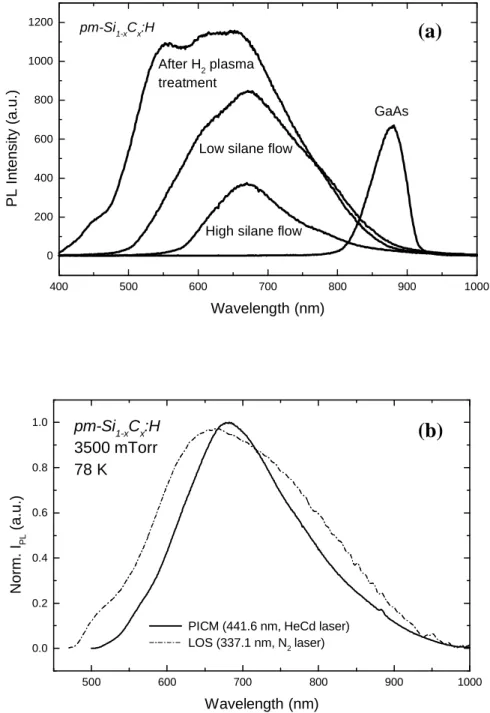
Among amorphous semiconductor materials, hydrogenated silicon-carbon alloys have been widely studied for the development of electroluminescent devices. The challenge of pm-Si1-xCx:H synthesis is to discover a feasible fabrication route that allows the growth of
improved luminescence materials that can be applied in optoelectronic and large area electronic devices. Indeed as shown in Fig. 1.1., pm-Si1-xCx:H films show quite impressive
luminescence properties, where the photoluminescence (PL) signal can be easily observed at Fig. 1.1. Red light emission of a pm-Si1-xCx:H film excited by a 4 mW HeCd laser at 325 nm.
room temperature with the naked eye. Electroluminescent device fabrication is another challenging task to accomplish, considering the carrier injection problem at the p/i or n/i interfaces and the low conductivity of the amorphous matrix in the intrinsic layer.
To determine the origin of the luminescence in polymorphous silicon carbon is one of the challenges of this thesis. Silicon nanocrystals and silicon nanoclusters are the main candidates for the luminescence source. Besides these sources, molecular luminescence sources such as siloxenes and polysilanes have also to be considered due to the existence of oxygen in the films and the high deposition pressure during fabrication. The contribution of the a-Si1-xCx:H
matrix, which is known to give luminescence [29-34], should also be considered. Moreover, if we recall the existence of defect states in the band tails as usually observed in amorphous materials, the luminescence can still be accepted as the process that might occur in the matrix even if there is an important difference between luminescence energy and optical band-gap energy (~0.5 eV). Furthermore, because the strong luminescent signal is observed at room temperature, the quantum confinement effect also becomes an important factor that should be evaluated as the origin of the luminescence.
Moreover, we have also observed a strong influence on the PL intensity of pm-Si1-xCx:H
by immersing the samples in liquid nitrogen. The difference between PL at 300 K in air and at 77 K in liquid N2 varies between one and three orders of magnitude. This cannot be explained by the change of temperature or by a change in the dielectric constant of the medium but is probably due to the passivation of defects. This effect describes well the potential of this material to be improved for many applications.
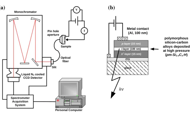
Electroluminescent devices
Electroluminescent devices based on amorphous silicon carbon alloys have been developed for more than 20 years. Towards that purpose, metal-insulator-semiconductor (MIS) structures [35], p-i-n structures [36, 37] and p-i-n structures with hot-carrier tunneling injection layers [38] have been studied. The realization of electroluminescent devices using pm-Si1-xCx:H as the active layer is a challenging task to accomplish, especially if we consider
the heterogeneous structure of this material, where the luminescence centers are the nanometer size crystallites inside the amorphous matrix. In this case, we have to take into account several problems related to the injection of carriers from the doped layers to the intrinsic layer and into the luminescence centers. The efficiency of the injection might be improved using known methods as described elsewhere [38-40], but the injection of carriers into the nanocrystals embedded in an amorphous matrix is still an open field. The surface
passivation of the nanocrystals, the difference in band-gap energy between the matrix and the nanoclusters, and the electric conductivity of the matrix, are important parameters to take into account to improve electroluminescent devices based on this material.
Table 1.1. Summary of silicon based light emitting materials. The characteristics of III-V and organic materials are also given as a comparison
Material Synthesis Method Structure Characteristics Year References
Porous c-Si Electrolysis Porous thin film on Si wafer
Room temperature, visible
emission, slow decay 1990 3
Porous a-Si Electrolysis Porous thin film on a-Si thin film
Room temperature, visible
emission 1996 7, 8
Nanocrystals Ion implantation + annealing
Embedded inside matrix
Room temperature, visible
emission, slow decay 1996 24-27
Nanocrystals Plasma (+annealing)
Embedded inside matrix or stand alone
Room temperature, visible
emission 1990 41, 42
a-Si clusters Plasma Embedded inside matrix
Room temperature, visible
emission 2001 9, 43
Siloxenes Chemical synthesis Thin film Room temperature, visible
emission 1992 11-14
Polysilanes Chemical synthesis Thin film Room temperature, visible
emission 1985 15-18 pm-Si1-xCx:H Plasma Aggregates of Si nanocrystals embedded inside amorphous silicon carbon matrix
Room temperature, visible emission, broad emission range, well encapsulated, slow decay
2004 44
c-Si Czochralski
technique Stand alone
Low temperature, indirect band gap, very low efficiency, near infra red (NIR) emission
1918 45, 46
a-Si:H Plasma Thin film Low temperature, low
efficiency, NIR emission 1978 47-50
pm-Si:H Plasma Thin film
Low temperature, low efficiency, red or NIR emission, absorption by matrix 1998 20-23 III-V Bridgmann method, LPCa, CVDb, MBEc, LPEd Stand alone
Room temperature, direct band gap, high efficiency, wide range UV-visible emission, fast decay
1955 45, 46
Molecular organics
Chemical synthesis
with OVPDe Thin film
Room temperature, high efficiency, wide range UV-Visible emission, lower stability than inorganic materials 1960s 51 f and refs. therein a
LPC (Liquid Encapsulated Czochralski) d LPE (Liquid Phase Epitaxy). b
CVD (Chemical Vapor Deposition). eOVPD (Organic Vapor Phase Deposition). c
MBE (Molecular Beam Epitaxy). fRecent review on the progress of molecular organic materials for electroluminescent applications.
References
[1] L. Canham, Nature 408, 411 (2000). [2] P. Ball, Nature 409, 974 (2001).
[3] L. T. Canham, Appl. Phys. Lett. 57, 1046 (1990). [4] Y. Kanemitsu, J. Lumin. 70, 333 (1996).
[5] L. Patrone, D. Nelson, V. I. Safarov, M. Sentis, W. Marine, S. Giorgio, J. Appl. Phys. 87, 3829 (2000).
[6] D. Kovalev, H. Heckler , M. Ben-Chorin, G. Polisski, M. Schwartzkopff, F. Koch, Phys. Rev. Lett. 81, 2803 (1998).
[7] R. B. Wehrspohn, J.-N. Chazalviel, F. Ozanam, I., Solomon, Phys. Rev. Lett. 77, 1885 (1996).
[8] R. B. Wehrspohn, J.-N. Chazalviel, F. Ozanam, I., Solomon, Thin Solid Films 297, 5 (1997).
[9] N. M. Park, C. J. Choi, T. Y. Seong, S. J. Park, Phys. Rev. Lett. 86, 1355 (2001). [10] K. Nishio, J. Koga, T. Yamaguchi, F. Yonezawa, Phys. Rev. B 67, 195304 (2003). [11] P. Deak, M. Rosenbauer, M. Stutzmann, J. Weber, M. S. Brandt, Phys. Rev. Lett. 69,
2531 (1992).
[12] H. D. Fuchs, M. Stutzmann, M. S. Brandt, M. Rosenbauer, J. Weber, A. Breitschwerdt, P. Deak, M. Cardona, Phys. Rev. B 48, 8172 (1993).
[13] M. Stutzmann, M. S. Brandt, M. Rosenbauer, J. Weber, H. D. Fuchs, Phys. Rev. B 47, 4806 (1993).
[14] R. F. Pinizzotto, H. Yang, J. M. Perez, J. L. Coffer, J. Appl. Phys. 75, 4486 (1994). [15] S. Furukawa, N. Matsumoto, Phys. Rev. B 31, 2114 (1985).
[16] R. D. Miller, J. Michl, Chem. Rev. 89, 1359 (1989).
[17] Y. Kanemitsu, K. Suzuki, Y. Nakayoshi, Y. Masumoto, Phys. Rev. B 46, 3916 (1992). [18] A. Kobayashi, H. Naito, Y. Matsuura, K. Matsukawa, H. Inoue, Y. Kanemitsu, Jpn. J.
Appl. Phys. 41, L1467 (2002).
[19] P. Roca i Cabarrocas, J. Non-Cryst. Solids 266-269, 31 (2000).
[20] A. Fontcuberta i Morral, H. Hofmeister, P. Roca i Cabarrocas, J. Non-Cryst. Solids 299-302, 284 (2002).
[21] S. Tchakarov, P. Roca i Cabarrocas, U. Dutta, P. Chatterjee, and B. Equer. J. Appl. Phys. 94, 7317 (2003).
[22] J. P. Kleider, C. Longeaud, M. Gauthier, M. Meaudre, R. Meaudre, R. Butté, S. Vignoli, P. Roca i Cabarrocas, J. Appl. Phys. 75, 3351 (1999).
[23] V. Suendo, A. V. Kharchenko, P. Roca i Cabarrocas, Thin Solid Films 451-452, 259 (2004).
[24] K. S. Min, K. V. Shcheglov, C. M. Yang, H. A. Atwater, M. L. Brongersma, A. Polman, Appl. Phys. Lett. 69, 2033 (1996).
[25] J. Linnros, A. Galeckas, N. Lalic, V. Grivickas, Thin Solid Fims 297, 167 (1997).
[26] M. L. Brongersma, A. Polman, K. S. Min, E. Boer, T. Tambo, H. A. Atwater, Appl. Phys. Lett. 72, 2577 (1998).
[27] M. L. Brongersma, P. G. Kik, A. Polman, K. S. Min, H. A. Atwater, Appl. Phys. Lett. 76, 351 (2000).
[28] L. Torrison, J. Tolle, D. J. Smith, C. Poweleit, J. Menendez, M. M. Mitan, T. L. Alford, J. Kouvetakis, J. Appl. Phys. 92, 7475 (2002).
[29] D. Engemann, R. Fischer, J. Knecht, Appl. Phys. Lett. 32, 567 (1978).
[30] W. Siebert, R. Carius, W. Fuhs, K. Jahn, Phys. Stat. Sol. (b) 140, 311 (1987).
[31] V. A. Vasil’ev, A. S. Volkov, E. Musabekov, E. I. Terukov, V. E. Chelnokov, S. V. Chernyshov, Yu. M. Shernyakov, Sov. Phys. Semicond. 24, 445 (1990).
[32] S. V. Chernyshov, E. I. Terukov, V. A. Vassilyev, A. S. Volkov, J. Non-Cryst. Solids 134, 218 (1991).
[33] C. Palsule, S. Gangopadhyay, D. Cronauer, B. Schröder, Phys. Rev. B 48, 10804 (1993). [34] L. R. Tessler, I. Solomon, Phys. Rev. B 52, 10962 (1995).
[35] H. Munekata, H. Kukimoto, Appl. Phys. Lett. 42, 432 (1983).
[36] D. Kruangam, T. Endo, G. Wei, H. Okamoto, Y. Hamakawa, Jpn. J. Appl. Phys. 24, L806 (1985).
[37] D. Kruangam, M. Deguchi, T. Toyama, H. Okamoto, Y. Hamakawa, IEEE Trans. Electron Devices 35, 957 (1988).
[38] S. A. Paasche, T. Toyama, H. Okamoto, Y. Hamakawa, IEEE Trans. Electron Devices 36, 2895 (1989).
[39] T. S. Jen, J. W. Pan, N. F. Shin, W. C. Tsay, J. W. Hong, C. Y. Chang, Jpn. J. Appl. Phys. 33, 827 (1994).
[40] J. W. Lee, K. S. Lim, Jpn. J. Appl. Phys. 35, L1111 (1996).
[41] H. Takagi, H. Ogawa, Y. Yamazaki, A. Ishizaki, T. Nakagiri, Appl. Phys. Lett. 56, 2379 (1990).
[42] H. Hofmeister, J. Dutta, H. Hofmann, Phys. Rev. B 54, 2856 (1996).
[43] H.-S. Kwack, Y. Sun, Y.-H. Cho, N.-M. Park, S.-J. Park, Appl. Phys. Lett. 83, 2901 (2003).
[44] V. Suendo, P. Roca i Cabarrocas, G. Patriarche, Optical Materials 27, 953 (2005).
[45] P. P. Yu, M. Cardona, Fundamentals of Semiconductors: Physics and Materials Properties, Springer-Verlag, Berlin, 1996.
[46] P. Bhattacharya, Semiconductor Optoelectronic Devices, Prentice-Hall, Inc., New Jersey, 1994.
[47] R. A. Street, J. C. Knights, D. K. Biegelsen, Phys. Rev. B 18, 1880 (1978). [48] K. M. Hong, J. Noolandi, R. A. Street, Phys. Rev. B 23, 2967 (1981).
[49] R. A. Street in J. I. Pankove (Ed.), Semiconductor and Semimetals Vol. 21 : Hydrogenated Amorphous Silicon Part B, Academic Press, Inc., Orlando, 1984, p197-244.
[50] H. Oheda, Phys. Rev. B 52, 16530 (1995).
Chapter 2
Experimental
2.1. Plasma Enhanced Chemical Vapor Deposition (PECVD)
Introduction
Plasma-enhanced (or -assisted) chemical vapor deposition (and etching), also called glow discharge because of the light emitted by the excited species, is an important technique for materials processing. It has been applied to the synthesis of new materials for optoelectronic applications including nanostructured materials, the fabrication of electronic devices, and the modification of surface and interface properties of materials. In recent years, plasma processes have become indispensable for manufacturing large area electronic devices, in addition to their crucial role in the processing of very large scale integrated circuits (ICs) for the microelectronics industry. Moreover, plasma processes are also critical in many other industries such as aerospace, automotive, steel, biomedical and toxic waste management [1]. In the case of hydrogenated amorphous silicon and related materials (SiC:H, SiGe:H, a-SiN:H,…) the RF glow discharge technique has become widely used because of its flexibility with respect to other deposition techniques [2].
By definition, a plasma is a ionized gas which remains electrically neutral from a macroscopic point of view [1, 3]. The presence of charged particles (electrons and ions) results in long-range Coulomb force interactions which are responsible for its unique properties. Industrial applications of plasma processes are mainly based on weakly ionized plasma discharges, characterized by the following properties: a) they are electrically driven, b) the collisions between charged particles and neutral gas molecules are important, c) there are boundaries at which surface losses are important, d) ionization of neutrals sustains the plasma in the steady state and e) electrons are not in thermal equilibrium with ions [1]. In the case of PECVD, the plasma processes are usually driven by an ac (alternating current) high frequency power supply, typically above 50 kHz and usually in the range of several megahertz or radio frequency (RF) range [1, 4]. The advantage of using high frequency excitation, compared to direct current plasma, is that a steady-state discharge can be sustained even with insulator coated electrodes, i.e., one can deposit insulating layers. This is possible
as the period of an RF half-cycle is shorter than the time needed for charging the insulator surface. This point is very important for applications where the glow discharge is used to deposit thin films on the surface of insulating materials (glasses, oxides, polymers, ceramics, etc.). Roughly, the electron density in RF discharges is of the order of 1015-1017 m-3 and electron temperatures (Te) in the range of 1- 4 eV, which of course depend on the dissipated power (typically 1-300 W) and on the gas mixture [1, 4].
Plasmas and Sheaths
A typical reactor for plasma process is a flat-bed or planar system in which the discharge is generated between two parallel plate electrodes (Fig. 2.1). In this system, one electrode is connected to the RF generator (RF / powered electrode or cathode) through an impedance matching network, which adapts the impedance of the system to 50 Ω, to ensure an optimal energy transfer to the discharge. The second electrode is usually connected to the ground (grounded electrode or anode). The choice of the electrode on which the substrate is mounted depends on the purpose of the process (deposition or etching), due to the difference in the energy of positive ions reaching the electrodes. The ion energy can be as high as VRF/2 for symmetric systems and as high as VRF at the powered electrode for asymmetric systems [1]. Therefore, the substrate is normally attached to the powered electrode for etching purposes, and to the grounded electrode for deposition.
In RF discharges, because they are electrically driven and weakly ionized, the applied power preferentially heats the mobile electrons with respect to ions. Due to their higher mass, ions efficiently exchange their energy through collision processes with gas molecules. On the other hand, the electrons cannot share the energy gained from the electric field through elastic collisions with heavier ions or neutral species due to their small mass. Hence, the electrons
Fig. 2.1. Schematic diagram of a flat-bed or planar RF discharge reactor.
RF Matching Network Grounded electrode Powered electrode Gas Discharge
reach a much higher average energy than ions (Te >> Ti). The electrons exchange their energy mainly through inelastic collision processes, such as excitation, dissociation and ionization. Therefore, the first step of plasma chemistry in RF discharges, the dissociation of gas molecules into radicals, is an electron driven process.
Sheaths are positively charged regions located between the bulk plasma (quasineutral, ni ne) and the walls. These layers are formed due to the losses of fast-moving electrons to the walls; note that the thermal velocity of electrons is at least 100 times that of ions. Thus, on a very short time scale, the loss of electrons to the walls forms a region with a positive net charge density near the walls. This leads to a potential profile that is positive in the bulk plasma and falls sharply to zero near the walls (see Fig. 2.2). This profile confines the traveling electrons to the bulk plasma and accelerates or pushes out the ions that enter the sheaths. This potential is defined as the plasma potential Vp, which is positive anywhere in the plasma and can be regarded as the reference potential of the system. The potential on the powered electrode is also negative with respect to the plasma potential Vp. This can be explained by the charging effect due the large difference in mobility between electrons and ions in the plasma, that results in a leaky diode I-V characteristic as shown in Fig. 2.3a [5]. An applied RF voltage induces a large electron current towards the powered electrode during one-half of the cycle and a small ion current on the second half of the cycle. As a result, the capacitively coupled RF electrode gets negatively charged up to a certain self-bias VDC, and finally the electron current induced by the positive voltage exceeding Vp on one-half of the
Fig. 2.2. Schematic diagram of average densities, electric field, and potential profiles after formation of the sheaths [1]. Plasma Sheaths n ni ne + + x x V Vp E E RF
cycle becomes equal to the net ion current on the other half of the cycle, when the electrode potential is lower than Vp. Fig. 2.3b shows the spatial distribution of the average potential in a RF discharge reactor, where the sheath potential, Vs, is equal to VDC + Vp on the powered electrode.
If we assume that the RF excitation is a perfectly sinusoidal wave, then we can derive a simple relation between the RF potential (VRF), the plasma potential (Vp) and the self-bias potential (VDC) [6]. Here, Vp is the most positive potential in the discharge by definition, then in the positive part of RF cycle we have
DC RF p
RF V V V
CV + ≥ + (2.1)
while in the negative part we have
0
≥ +
−CVRF Vp (2.2)
If we consider only the equality from equation 2.1 and 2.2, then by elimination we can obtain
(
DC RF)
p V V
V = 21 + (2.3)
Equation 2.3 expresses a simple relation that can be used to estimate the plasma potential from observable potentials, which are easy to measure.
Deposition parameters and PLASMAT reactor
In the RF discharge deposition process we can measure and adjust several parameters which are important for the process control. Some of them are usually recorded as indicators,
Vp VDC Vs + V 0 - V Substrate holder (grounded electrode) RF electrode P o te n ti a l Voltage Plasma I-V Electron current Ion current C u rr e n t RF signal VDC a) b)
Fig. 2.3. Schematic diagram of a) generation of negative self-bias on the powered electrode in contact with RF plasma and b) spatial distribution of average potential in a RF glow discharge flat-bed reactor [6].
such as the self-bias potential (VDC) and the RF potential (VRF). The other parameters can be categorized into i) adjustable parameters such as total pressure, partial pressure, gas flow rates, substrate temperature, RF power, plasma excitation frequency and ii) reactor geometry related parameters (distance between electrodes, electrodes diameter, and surface ratio of powered to grounded electrodes). By changing these parameters, we can optimize the deposition conditions to obtain materials with desired properties.
In this work, we have used a flat-bed PECVD reactor (PLASMAT reactor), equipped with in-situ diagnostics providing information on the process itself: optical emission spectroscopy (OES), plasma impedance monitoring system (PIM), self-bias and RF potential measurements (Fig. 2.4), and on the material properties via a UV-Visible spectroscopic ellipsometer. This reactor preferentially works at a plasma excitation frequency of 13.56 MHz in the pressure range of 30-5000 mTorr. The temperature of each electrode can be independently adjusted in the range of 25-300 °C. The installed feed gases are H2, Ar, He, SiH4, CH4, PH3 diluted in H2 and trimethylboron (TMB) diluted in H2. The self-bias potential is measured using a low-pass filter connected to a voltmeter (multimeter), while the RF potential is measured through a calibrated dividing capacitor [7]. The details of other characterization techniques will be explained in the next sections.
RF Matching Network Personal Computer Light Source Monochromator Spectralink Hot substrate Electrode RF Gas Modulator Analyzer or collimating lens Water or liquid N2 Cold substrate or OES System PIM Multimeter/ oscilloscope Impedance/VPP/VDC probe a) b)
Fig. 2.4. PLASMAT reactor : a) a schematic diagram of installed in-situ diagnostic measurement systems, including a water or liquid nitrogen cooled substrate holder; b) front view of the reactor and the working environment.
Plasma Studies
2.2. Optical Emission Spectroscopy (OES)
Introduction
Optical emission spectroscopy (OES) of gas discharges has been long used for qualitative and quantitative analysis in plasma physics and chemistry. Information on the excited species in the plasma, including their intensity and relative changes with respect to other excited species can be obtained using this technique, which gives a rough idea of species concentration in the plasma. In practice, the excited species responsible for emission are not necessarily the most relevant for the deposition process. Measured OES quantities should therefore be considered as qualitative. To obtain quantitative information one must use more sophisticated methods such as actinometry and laser induced fluorescence, which are beyond the scope of this study.
In the plasma, electrons are responsible for almost all excitation and dissociation processes since they are much lighter than other species, which makes it easier for them to gain energy from the applied power. Moreover, ion bombardment, chemical reactive recombination, and metastable energy transfer can also contribute to the emission processes. Thus, plasma emission can result from following mechanisms:
a) electron impact excitation,
hv A A e A e A + → + → + − − * *
b) electron impact dissociation,
hv A A e B A e AB + → + + → + − − * *
c) ion impact processes,
hv A A M A M e A + → + → + + − + * * ) ( ) (
hv AB AB C AB BC A + → + → + * *
where A, B and C are atoms or molecules, * indicates the excited (emitting) species, e- is an electron and e-(+M) may be a neutral species, a negative ion, an electron plus a third body, or a surface (e.g. electrodes, reactor walls or particles in the plasma) [8].
Experimental setup and data treatment
The experimental setup for this technique is quite simple. It consists of i) a collimating system to collect the emission signal, ii) a optical fiber that brings the collected signal to the monochromator, iii) a high resolution monochromator with an adjustable entrance slit and iv) a photodetector. A detailed setup of this technique is explained elsewhere [5]. In practice, it is installed in our PECVD reactor (see Fig. 2.4a) with detail shown in Fig 2.5.
In this study, we used OES as a semi-quantitative technique to analyze the relative amounts of species in the plasma. Thus, we studied the evolution of the emission intensity of the species of interest, or the ratio of one species relative to another from one plasma condition to another. Each spectrum is baseline corrected with respect to the measurement background. Further, other data treatments are necessary as well, such as numerical integration to analyze the peak surface area (integrated intensity) and peak fitting using
Spectrometer equipped with liquid nitrogen cooled CCD detector 35° Optical window Collimating system Fiber optic RF electrode grounded electrode (substrate holder) sample Plasma
Fig. 2.5. Schematic of the setup for plasma optical emission spectroscopy (OES) measurements in PLASMAT reactor (see fig 4.24a). The optical window, also used for spectroscopic ellipsometry measurements, has a diameter of 0.8 cm and its axis is at 35° from the normal of substrate holder.
Lorentzian function to obtain the full width at half maximum (FWHM) and other fitting parameters of the curves.
SiH4-CH4-H2 glow discharge
Fig. 2.6 shows typical OES spectra from a RF glow discharge in pure hydrogen a) and a SiH4-CH4-H2 mixture b). The emission lines of these systems are summarized in Table 2.1.
Table 2.1. Emission lines in SiH4-CH4-H2 RF glow discharge system.
Line/band Transition Wave length (nm) Note Reference
Balmer Hα n'=3→n=2 656.2 Balmer Hβ n'=4→n=2 486.1 Balmer Hγ n'=5→n=2 434.0 Balmer series:
(
2 2)
1 2 1 n R − = ν n=3, 4, 5,…; R=Rydberg const. 5, 9, 10, 11, 13, 14SiH* A2∆→X2Π 414.2 Analogous to CH (A-X) system 5, 12, 13,
15
C2 Swan d3Πg →a3Πu
516.5 Swan band of C2 11, 14
CH* 2∆→ 2Π
X
A 431.4 CH (A-X) system with Q (0,0)
band head at 431.4 nm 9, 10, 11, 12, 14 H2 Fulcher-α d Πu →a Σg 3 3
570-640 Broad band consists of many
lines centered at 602 nm 5, 10, 11, 14 350 400 450 500 550 600 650 700 750 800 b) SiH 4-CH4-H2 Wave length (nm) a) H 2 Intensity ( a.u.) Balmer Hα H2 Fulcher-α bands CH* SiH*
Fig. 2.6. Typical optical emission spectra of RF discharge plasmas with the emission lines of interest at 1600 mTorr for a) pure hydrogen and b) SiH4-CH4-H2 mixture with an RF power of 10 and 20 W respectively. The temperature of both electrodes was set at 200 °C.
2.3. Plasma Impedance Analysis
Introduction
Plasma impedance analysis is a sensitive and portable analysis method used to detect the present of nanometer size particles in capacitively coupled radio-frequency (RF) discharge at 13.56 MHz [16]. This method is based on the fact that the discharge is non-symmetric and capacitive-like, thus showing a non-linear relation between the RF voltage and the RF current in the sheaths [1]. This non-linearity induces the generation of harmonics in the discharge current that give significant information about the dynamics of ions and electrons in the plasma. When nanometer size particles are present in the plasma, the third harmonic (40.68 MHz) of RF current, J3, has been shown to give the most significant changes as a function of time [16]. The abrupt changes on the amplitude ratio of the third harmonic of the RF current to the fundamental one (J3/J0) are also observed in the so-called α-γ’ transition, which is accompanied by the appearance of particles and powders [13]. These abrupt changes are
observed as a decrease of the amplitude ratio by one order of magnitude as the plasma changes fromα toγ’ mode, while the ratio between the first harmonic to the fundamental one almost does not change. The observed changes are related to the modification of the electron collision frequency in the discharge by the electron-particle collision process, which is proportional to the concentration and the collision cross section of particles. Moreover, the
Fig. 2.7. Time evolution of the amplitudes of the third harmonic of the RF current for a) particle-free argon plasma and b) a powder-forming argon-silane plasma [16].
particles in the plasma act as electron ‘traps’ through the electron attachment process [16, 13]. This process perturbs the electron-energy distribution function and self-sustaining electric field, which is observed as a decrease in the amplitude of J3, related to the increase of plasma resistance. In the following, we use the amplitudes of the third harmonic of RF current as the observable parameter to monitor the presence of particles in the plasma, which we have confirmed by laser light scattering measurements in our reactor [17].
Particle growth monitoring
Fig. 2.7 shows the time evolution of the amplitudes of the third harmonic of the RF current, which represents the particles growth timeline in the plasma [16]. In general, this time evolution can be divided into 3 regions: i) gas decomposition region (t0<t<t1), which starts when the plasma is turned on and reaches a plateau; ii) particle formation and accumulation regime (t1<t<t2); and iii) coagulation regime or powder formation regime (t>t2). In general, the experimental setup for this technique consists of i) an RF voltage probe, ii) an RF current probe, iii) an electronic board to process the measured signals, and iv) a personal computer with controlling applications to monitor and visualize the measured results. This
probing system is installed at the entry of the RF power in a PECVD reactor (between the matching network and the cathode) as shown schematically in Fig.2.4a. Recently, comparative studies between the time evolution of the self bias potential (VDC) and the amplitude of the third harmonic of the RF current (J3) have shown good [18]. Thus, we can use the evolution of VDC instead of J3 to monitor the formation of particles and powder in the
0 1 2 3 4 5 6 0.015 0.020 0.025 0.030 0.035 0.040 1800 mTorr SiH4 + H2 with TMB 50 mTorr with PH3 50 mTorr J3 ( A) t (s) 0 1 2 3 4 5 6 -60 -55 -50 -45 1800 mTorr SiH4 + H2 TMB 50 mTorr PH3 50 mTorr VDC ( V) t (s) a) b)
Fig. 2.8. The comparison between the time evolution of a) the amplitude of the thirdd harmonic of RF current (J3) and b) the self-bias potential (VDC) for a SiH4-H2 mixture plasma in the powder formation regime: 1800 mTorr with temperature of electrode of 200 °C and RF power of 22 W.
plasma. In Fig. 2.8 we compare the evolution of J3 and VDC for SiH4-H2 systems with and without doping gas in the powder formation regime at 1800 mTorr.
Materials Characterizations
2.4. Phase Modulated UV-Visible Spectroscopic Ellipsometry (SE)
Basic principle and experimental setup
Ellipsometry is a powerful technique for determining the thickness and optical properties of thin films [19, 20]. It is based on the principle that a fully polarized light changes its polarization state after reflection from or transmission through a thin film [21]. In general, ellipsometry can be used to measure both the index of refraction and the thickness of either transparent or absorbing materials. By examining the polarization state of the reflected light of known polarization, wavelength, and angle of incidence, we can obtain the information on the optical properties of thin films. Moreover, due to its non-perturbing nature, this technique is also very useful for in-situ studies during deposition.
The polarization state of the reflected light can be represented by the following complex number [21, 22]:
Fig. 2.9. Schematic diagram of incident, reflected and transmitted light on thin slab
i p E i s E t s E t p E r p E r s E t k r k i k φ
( ) ( )
∆ = = i r r s p exp tan ρ (2.4)where ψ and ∆ are the ellipsometric angles. rp and rs are the parallel and perpendicular
reflection coefficients (Fresnel coefficients):
i p r p p E E r = (2.5) i s r s s E E r = (2.6)
where Eyxare the electric field vectors as shown schematically in Fig. 2.9. (x = i for the
incident, x = r for the reflected and x = t for the transmitted waves respectively; y = p for parallel component and y = s for perpendicular component to incident plane).
The experimental setup of the phase-modulated UV-Visible spectroscopic ellipsometer (UVISEL) is represented schematically in Fig. 2.10. In this setup, the white light from the source is first modulated linearly by a polarizer then elliptically by a photo-elastic modulator. In this case the phase shift between component Es and Ep isδ(t), can be expressed as
Fig. 2.10. Phase modulated UV-visible ellipsometer setup Personal Computer 0 θ i s E i p E r p E r s E UV-visible light source Polarizer Modulator photo-elastic Sample Analyzer Spectrometer Photomultiplier tube
( )
t = Asin( )
tδ , where 50kHz
2π = (2.7)
The reflected light is analyzed by a linear polarizer then its intensity is measured at selected wavelengths by a photodetector attached to a monochromator. The measured intensity I is defined as
( )
t I I( )
t I( )
t I J( )
AI t J( )
A I tI λ, = 0 + ssinδ + ccosδ ≅ 0 +2 1 ssinω +2 2 ccos2ω (2.8)
where Ji is the ith order Bessel function. Is and Ic are defined as,
( )
+ = ∆ = * * * Im 2 sin 2 sin p p s s p s s r r r r r r I (2.9)( )
+ = ∆ = * * * Re 2 cos 2 sin p p s s p s c r r r r r r I (2.10)By Fourier analysis of the signal, we can obtain directly the values of Is and Ic, which relate to
the Fresnel coefficients of the sample.
Data treatment and interpretation
In order to analyze quantitatively a spectroscopic ellipsometry measurement, we have to fit the experimental spectrum using an optical model. To obtain the best fit condition, we used the Levenberg-Marquardt algorithm to minimize globally the value of the biased estimator
χ2
(θ). Hereχ2(θ) is a merit function that ensures the best fit of the SE data to the model at its global minimum. The biased estimatorχ2(θ) is defined as
( )
∑
(
)
( )
(
)
( )
= − + − = N k k k mes k sim k k mes k sim Is Ic Ic Is N 1 2 2 2 2 2 , , 2 1 (2.11)In the general case of thin films, an optical model should contain information about: i) experimental parameters (angle of incidence, substrate, dielectric function of ambient), ii) film structure (how many distinguishable layers and their thickness), iii) layer structure (homogeneous, heterogeneous, isotropic, non-isotropic or gradual layer), and iv) dielectric function of each layer. The dielectric function of each layer can be expressed by the dielectric function of a single material or by a mixture of several materials, based on the effective medium theory. In general the effective medium theory can be expressed by the following equation [24]:
(
)
(
)
,( )
1 k 1 − = + + + + = q a b b a h b b a a h b a k f f f f k , 0≤q≤1 (2.12)where q is the screening parameter; ε, εh, εa and εb are the dielectric function of composite
material, host material, component a and component b respectively; fa and fb are the volume
fraction of components a and b respectively. In our case, we use Bruggeman effective medium approximation (BEMA), which is defined using eq. 2.12 withεh =ε and q = 1/3 (or k
= 2). The BEMA represents most likely an aggregate microstructure in which neither component can be viewed as the host material. The dielectric function of a single material can be expressed by a standard based on the experimental data or by a mathematical model whether it is derived theoretically (all involved parameters have physical meaning) or not (empirically, only a mathematical expression that allows to reproduce the experimental results).
In the case of amorphous silicon derived materials, the raw experimental data can be described by a two-layer model (ambient/surface roughness/bulk layer/substrate) as shown schematically in Fig. 2.11. From an optical point of view, the surface roughness (5-30 Å thick) is modeled by a layer with equivalent parallel-plane boundaries whose thickness is
Substrate Bulk layer
Substrate Bulk layer 50 % Void / 50 % Bulk layer
Surface roughness
equal to the characteristic roughness height parameter [21], and whose optical properties are described as a mixture of those of the bulk layer and ambient (void) according to the effective medium theory. In order to reduce the number of fitting parameters, we have kept the composition of the surface roughness constant (50 % void + 50 % bulk layer). Indeed, it has been shown empirically by Fujiwara et al [24] that in some cases we can replace this layer by a mixture of voids and bulk layer a fixed composition ratio of 1:1. The bulk layer is modeled as an homogeneous amorphous layer using the Tauc-Lorentz dispersion law [25]. This model combines Tauc's law for photon absorption above the band edge of amorphous semiconductors [26] and the standard quantum mechanical approach, thus the imaginary part of the dielectric function is expressed by the following equation:
(
)
(
)
g g g E E E E E E C E E E E C AE ≤ = > ⋅ + − − = 0 , , 1 2 2 2 2 0 2 2 0 2TL (2.13)Where A is the amplitude factor proportional to the density matrix of the material and the optical transition matrix elements, E0 is the peak transition energy, C is the broadening
parameter and Eg is the optical band gap. The real part of the dielectric constant is obtained by
Kramers-Kronig integration, given by
( )
(
)
(
)
(
)
+ − + ⋅ − + + − + ⋅ − − + − ⋅ + + + + − ⋅ − − + + + ⋅ + ∞ = 2 2 2 2 2 0 4 0 2 2 4 0 2 2 2 2 4 0 g g 0 atan 4 2 2 0 2 2 0 0 ln 4 1TL 1TL ln 2 ln 2 atan 2 2E -atan 2E atan ln 2 C E E E E E E E E C AE E E E E E E E C AE C E E E AE C C E a A E E E E E E E a AC g g g g g g g g g g g g g g (2.14) where(
)
(
2 2)
0 2 0 2 2 2 2 0 2 ln Eg E E EgC E E 3Eg a = − + − + (2.15)(
)(
2 2)
2 2 0 2 0 2 atan E E E E E C a = − + g + g (2.16)(
)
4 2 2 2 2 2 4 C E − +α = (2.17) 2 2 0 4E −C = α (2.18) 2 / 2 2 0 C E − = γ , (2.19)which adds another free parameter, the high frequency dielectric constant, ε1 ). Fig. 2.12a. shows the real and imaginary parts of the pseudo-dielectric function of a polymorphous silicon carbon alloy deposited on corning glass. The spectra are fitted considering a two-layer model. In this case, the dielectric functions are modeled using the Tauc-Lorentz model for the bulk layer and a 1:1 ratio of bulk material over void with BEMA the surface roughness, as
1,5 2,0 2,5 3,0 3,5 4,0 4,5 5,0 0 2 4 6 8 10 εr εi
ε
r,
ε
iPhoton energy (eV) -8 -4 0 4 8 12 16 εr (exp) εi (exp) εr (fit) εi (fit)
<
ε
r>
,
<
ε
i>
Fig. 2.12. Experimental and modeled real and imaginary parts of the pseudo-dielectric function of a pm-Si1-xCx:H film deposited at 3500 mTorr (200 °C), using a two-layers model with
surface roughness consisting of 50 % of void and 50 % of bulk layer material (a) and extracted bulk layer dielectric function (b). The fitting parameters are: Eg=2.30 eV, ε1 )=1.82, A=127.22 eV, E0=3.86 eV, C=3.57 eV and thickness of bulk layer of 2970 Å.
(a)
described above. The extracted dielectric function for bulk material, free of interference fringes due to multiple reflections and surface roughness effects, is shown in Fig. 2.12b. In this study, the deposition rate was determined from film thickness and deposition time by taking the assumption of an homogeneous constant film growth. For more detail on this technique, a review that covers general information and deeper discussions on in-situ studies of thin film growth can be found in ref. 19.
2.5. Raman Spectroscopy
Introduction
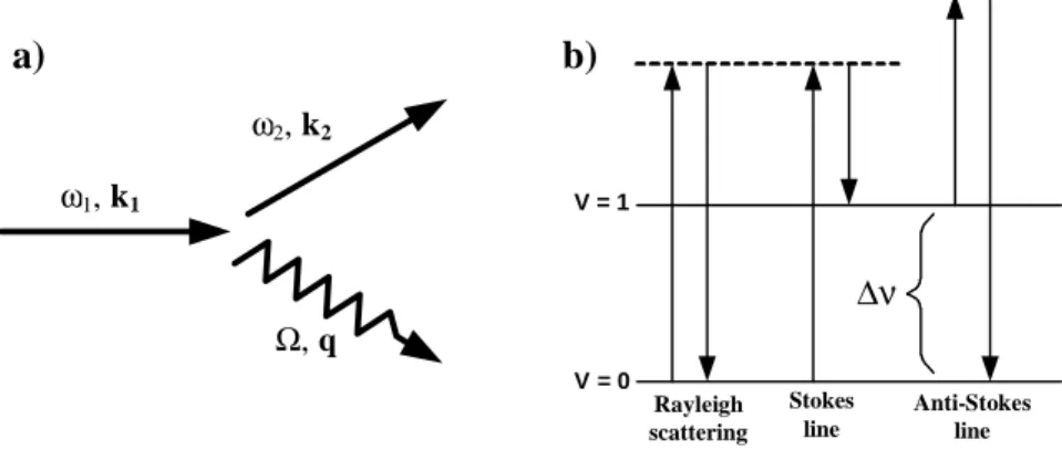
When photons interact with a molecule, they may be absorbed or scattered. Scattering itself is defined as a phenomenon in which photons change their direction and possibly also their energy after interaction with matter. Further, light scattering can be classified into elastic and inelastic processes, which describe the phenomena by which the photons are scattered without and with changes of their energy respectively. The inelastic scattering process is illustrated in Fig. 2.13a, where light incident with angular frequency ω1 and wave vector k1 is scattered as a photon with frequencyω2 and wave vector k2 by an excitation of the medium of
frequency Ω and wave vector q [27]. This type of scattering can be mediated by many
different types of elementary excitations in the matter. However, in the case of Raman
scattering, we will consider only phonon mediated processes, which correspond to the energy difference in the vibrational and rotational energy levels. In this case, there is a similarity between Raman and infrared spectra, even though they are not the same due to the differences in the selection rules and relative band intensities. For a molecular vibration to be Raman
V = 0 V = 1 ∆ν Rayleigh scattering Stokes line Anti-Stokes line ω1, k1 ω2, k2 Ω, q a) b)
active, there must be a change in the induced dipole momentum as a result of a change in the polarizability of the molecule [28]. Therefore, even if there is no change in the dipole momentum or the molecule has no permanent dipole, it still can be Raman active as long as it has a change in the polarizability or in the induced dipole momentum due to vibrations or rotations. In general, the inelastic scattering can be divided in two generic types such: Stokes and anti-Stokes scattering (Fig. 2.13b). Stokes scattering corresponds to the emission of a phonon (scattered photons lose their energy), while anti-Stokes scattering corresponds to phonon absorption (scattered photons gain energy). Thus, with respect to the exciting photon energy, the light is shifted down in energy during a Stokes process and up in an anti-Stokes event.
Experimental setup and data treatment
A schematic diagram of a Raman setup equipped with a microscope for micro-Raman measurements with a HeNe laser (632.8 nm) as the source of excitation is shown in Fig. 2.14a. In this setup, the reflected part of the excitation light is cut off by a notch or edge filter instead of a second monochromator. The experimental spectra of Raman measurements were treated by fitting the data over the range of interest as a deconvolution of several Gaussian functions. From the fitting, we can obtain the area and the full width at half maximum (FWHM) for each peak, which provides information on each mode of vibration. Fig. 2.14b shows a typical Raman spectrum of hydrogenated amorphous silicon. We can observe the
Spectrometer Acquisition System Personal Computer CCD Detector Sample Optical fiber Monochromator Slit
Optical microscope with Long wave pass filter
H e N e L a s e r 0 200 400 600 800 1000 1200 1400 1600 0 5000 10000 15000 20000 25000 2TO Si-H TA LA LO TO Raman Intensi ty (a.u.) Wave number (cm-1)
a)
b)
Fig. 2.14. a) A schematic diagram of a micro-Raman system and b) a typical Raman spectrum of a
principal phonons of amorphous silicon: i) transverse optic (TO) at 480 cm-1, ii) longitudinal optic (LO) at 380 cm-1, iii) longitudinal acoustic (LA) at 310 cm-1, and iv) transverse acoustic (TA) at 150 cm-1 [28]. Moreover, the Si-H vibration mode at 640 cm-1 and the 2nd harmonic of the TO phonon at 960 cm-1 are also shown [29].
2.6. Infrared Spectroscopy
Introduction
The energy of a molecule can be divided into four parts, which are: a) translational energy, b) rotational energy, c) vibrational energy and d) electronic energy [28]. Electronic energy transitions normally are responsible for the absorption or emission in the UV and visible regions, while molecular vibrations give rise to the absorption through out most of the infrared region. When the frequency of a specific vibration is equal to the frequency of the IR radiation, the molecule will absorb the radiation with some selection rules. The simplest representation of a molecular vibration is the oscillation of a diatomic molecule, where its potential energy depends on the intermolecular distance. For a mode of vibration to be infrared active, there must be a change in the dipole moment of the molecule when it vibrates [28, 31]. Therefore, most symmetric stretching vibration modes of symmetric molecules are infrared inactive, while asymmetric modes are infrared active.
In this study, we used a Fourier-transform infrared spectrometer (FTIR), which measures the IR absorption in the range of 500-4000 cm-1 with a resolution of 2 cm-1. This instrument consists of three basic components: a radiation source, an interferometer and a detector. The main difference in the setup between an FT and dispersive spectrometer systems is the replacement of the monochromator by an interferometer. The interferometer divides light into two beams, generates an optical path difference between them, then recombines them to produce repetitive interference signals as a function of optical path difference by a detector. In short, it produces interference signals that contain infrared spectral information generated after passing through the sample. A detailed description of the setup is explained elsewhere [31].
Data treatment and analysis
In order to analyze the data from FTIR measurements, first we have to eliminate the interference fringes from the raw data. In this study, we followed a quantitative method developed by Maley [32]. In this procedure, we fit the interference fringes of the spectra using
an optical model that considers a thin film on a semi-infinite substrate (c-Si) with multiple reflections (Fig. 2.15) as follows:
(
31 34)
13 34 1 R R T T TNA − = (2.20)in the coherent limit, we have
(
)
2 23 21 2 23 12 1 3 13 1 / r r P P t t n n T − = (2.21) 2 23 21 2 23 21 12 2 12 13 1 P r r r t t P r R − + = (2.22) 2 23 21 2 21 23 32 2 32 31 1 P r r r t t P r R − + = (2.23) where for j =i±1 j i i ij N N N t + = 2 (2.24) j i j i ij N N N N r + − = (2.25) 2 ij ij r R = (2.26) 2 ij i j ij t n n T = (2.27)(
πiN dω)
P=exp −2 2 (2.28) Medium 1 (Air) N1= 1 - i0 Medium 2 (Films) N2= n2- ik2 Medium 4 (Air) N4= 1 - i0 Medium 3 (Substrate) N3= n3 i0Fig. 2.15. Schematic diagram of the multiple reflections of an absorbing film on a non absorbing substrate. Here, the multi reflections in the substrate are omitted and the light is shown at non-normal angle of incidence for clarity [29].
i i
i n k
N = − (2.29)
By applying eqs. 2.20-2.29, we can fit the experimental data and obtain the base line with the interference fringes (Fig 2.16a). Here, we applied n3= 3.42 for the c-Si substrate, while n2 of the films are pre-determined through spectroscopic ellipsometry measurement then extrapolated to low energy. These values of n2 are included later on into the fitting parameter to obtain more precise values. Using the baselines obtained here, we can eliminate the interference fringes and obtain an interference-free transmission spectra (Fig. 2.16b).
In order to calculate the absorption coefficient (α) from the interference-free transmittance, we followed the procedure proposed by Brodsky et. al. using the following relations [33]:
(
)
d d e R e R T α α 2 2 2 1 1 − − − − = (2.30)where d is the film thickness and R is an empirically determined interface multiple reflection loss. Here, we determined R by setting T = T0 = 0.54 as the absorption-free transmission of c-Si substrate whenα = 0 [32, 33], which yields
4000 3500 3000 2500 2000 1500 1000 500 0.40 0.42 0.44 0.46 0.48 0.50 0.52 0.54 0.56 (b) Wave number (cm-1) 0.45 0.50 0.55 0.60 0.65 0.70 (a) Baseline Raw data Transmittance
Fig. 2.16. Transmission spectra of pm-Si1-xCx :H deposited at 800 mTorr with an RF power
of 20 W : a) raw spectrum with baseline as fitting result of eq. 2.20 from ref. 29 and b) baseline corrected spectrum.
0 0 1 1 T T R + − = (2.31)
then by substituting eq. 2.31 into eq. 2.30, we can obtain
(
) (
)
d d e T T e T T α α 2 2 0 2 0 2 0 1 1 4 − − − − + = (2.32)which can be used to calculate α from the baseline corrected transmittance. We note that this procedure is still valid for samples with large index mismatch with respect to the c-Si substrate, such as pm-Si1-xCx:H thin films, as long as the interference elimination is applied with the exact equation of non-absorption transmittance as written in eq. 2.20. In principle, Maley’s interference fringes elimination procedure transforms the raw data series which contains an unknown function T0 = f(ω) as T0 = 0.54 (see Fig. 2.16).
Further, using the data of IR absorption coefficient spectra, we can calculate the bond concentration for each type chemical bond in our films. The bond concentration for X-Y chemical bond (NX-Y) is related to the integrated absorption of its peak by
( )
ω ω ω α d A NX−Y =∫
(2.33)where A is the proportionality factor or absorption strength and ω is the frequency or wave number in cm-1[33-36]. The values of A for chemical bonds of interest in pm-Si1-xCx:H films
are considered to be similar to these reported for a-Si1-xCx:H alloys and are tabulated in Table
2.2.
Table 2.2. IR absorption strength of chemical bonds in pm-Si1-xCx:H films.
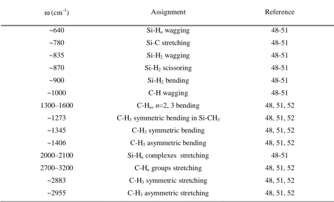
Chemical bond ω (cm-1) A (cm-3) References
Si-C 780-810 2.13 × 10¹⁹ 37, 38
Si-H 2000-2150 1.4 × 10²⁰ 34, 35, 37, 38
C-H 2850-2950 1.35 × 10²¹ 37, 38
2.7. Photoluminescence (PL) Spectroscopy
Basic principle and experimental setup
In order to have a sample that emits photons, it has to be excited by some external source of energy. The method of excitation leads to a classification of the emission process. In the case of semiconductor materials, one possible method is the injection of electrons and