Silicon nitride waveguide optical filter components for access
network applications
by
Saurabh BEDI
THESIS PRESENTED TO ÉCOLE DE TECHNOLOGIE SUPÉRIEURE
IN PARTIAL FULFILLMENT FOR A MASTER’S DEGREE
WITH THESIS IN ELECTRICAL ENGINEERING
M.A.Sc
MONTREAL, OCTOBER 19, 2018
ÉCOLE DE TECHNOLOGIE SUPÉRIEURE
UNIVERSITÉ DU QUÉBEC
This Creative Commons licence allows readers to download this work and share it with others as long as the author is credited. The content of this work can’t be modified in any way or used commercially.
BOARD OF EXAMINERS (THESIS M.A.SC.) THIS THESIS HAS BEEN EVALUATED BY THE FOLLOWING BOARD OF EXAMINERS
Mr. Frédéric Nabki, Thesis Supervisor
Department of Electrical Engineering, École de technologie supérieure
Mr. Michaël Ménard, Thesis Co-supervisor
Computer Science Department, Université du Québec à Montréal
Mr. Ricardo Izquierdo, Chair, Board of Examiners
Department of Electrical Engineering, École de technologie supérieure
Mr. Bora Ung, Evaluator
Department of Electrical Engineering, École de technologie supérieure
THIS THESIS WAS PRENSENTED AND DEFENDED
IN THE PRESENCE OF A BOARD OF EXAMINERS AND PUBLIC SEPTEMBER 28TH, 2018
ACKNOWLEDGMENT
Firstly, I would like to thank my family for their unceasing support, encouragement and faith throughout my period of study. Their unwavering support has helped me throughout my studies since childhood until now. Secondly, I would like to thank few individuals without whom this project would have not been successful. Their constant help and supervision have helped me reshaping my thesis and evolved me as a researcher. I sincerely thank my supervisor Prof. Frederic Nabki (ETS) and my co-supervisor Prof. Michael Menard (UQAM) for their unwavering support, faith and guidance throughout my research project. Their assistance has been profitable from time to time and have been enlightening during the difficult times. Their faith in me have pushed me through my difficult times. Thirdly, I would like to thank Mr. Francois Menard and Mr. Philippe Babin from our industrial partner AEPONYX for believing in me and trusting me with this challenging research work. My research team members from CoFaMic research center, UQAM who have helped me in the fabrication and characterization of my design chips. I would personally like to give a quote of thanks to Dr. Menouer Saidani for helping me out in fabricating my device structures, Dr. Hadi Rabbani Haghighi for his technical guidance and sharing his expertise in the field of optics during the initial period my master thesis, Dr. Mohannad Alsayedfor being the fabrication expert of our group and advising about the fab techniques and constraints. My wife Sakshi Jain whose constant support and love has pushed me this far and has helped me during the challenging time of my research. My colleagues Mr. Suraj Sharma (PhD student) working on MEMS platform for his moral support throughout my research period and Mr. Belaid Tabti (Master student) at UQAM for his support and knowledge exchange during the technical projects and while my initial challenging phase with measurements of the devices. Their consistent support has allowed me to finish my time-bound projects and to achieve my targets within the research timeline. Also, I would like to acknowledge some other personnel’s who have been a healthy part of my journey, in one way or the other, during my master thesis project such as Dr. Michiel Soer (CoFaMic), Mrs. Anubha Gupta Soer (PhD student), Mr. Shivaram Arun (PhD student), Mrs. Devika Padamkumar Nair (PhD student) for their light hearted conversations over coffee and maintaining an incredible research environment.
VI
I gratefully acknowledge the support of the National Sciences and Engineering Research Council (NSERC) of Canada. Also, I would take this opportunity to thank our other research partners such as Regroupement Stratégique en Microsystèmes du Québec (RESMIQ) and Centre d’ Optique, Photonique et Laser (COPL). In the end, I would like to acknowledge CMC Microsystems for the provision of services that facilitated this research and Lumerical Solutions, Inc. for providing the design tools
SILICON NITRDE WAVEGUIDE OPTICAL FILTER COMPONENTS FOR ACCESS NETWORK APPLICATIONS
Saurabh BEDI
ABSTRACT
Silicon nitride (SiN) waveguide based micro ring/racetrack resonators to be used as filters in the Chirp Managed Lasers (CMLs) are modelled and demonstrated over the standard silicon (Si) wafer. The development of these racetrack-resonators, with a narrow free spectral range (FSR) of 100GHz is in correspondence to the international telecommunication union (ITU) recommended channel grid spacing required for the latest next generation passive optical networks (NGPON2) systems. The study of such optical filters, which tend to increase the transmission range of the directly modulated laser (DML) signal, is motivated from the research and development directed towards bringing the CMLs to a reality. Also, a single SiN ring resonator and a silicon waveguide based cascaded 3-ring design, both integrated within the Y-splitter configuration are presented to be used as a reflector in external cavity laser. These ring reflectors are designed to have a broad FSR, which is achieved using the Vernier effect by serially coupling three racetrack resonators. In this thesis, we analyze and optimize the optical response of the above mentioned devices based on SiN waveguides deposited over silicon wafers. The design parameters are optimized based on analytical modelling and simulations are carried out with finite difference time domain (FDTD) solver. The devices are fabricated in different labs and clean room facilities within Montreal in collaboration with our industrial partner AEPONYX. The performance of these fabricated devices is characterized using an optical test setup in university lab facilities. The simulation and the measurement results are in close proximity for a large 4-port add-drop racetrack resonator, giving a FSR close to 100GHz specified for the NGPON2 systems and an extinction ratio (ER) of >15 dB to be useful for modulating the inherent chirp of the directly modulated lasers (DML) and thereby increasing the transmission range of the data signals. For the Si waveguide based cascaded 3rd order ring reflector, a wide FSR of 90.2 nm is achieved numerically and a FSR of around ~6.02 nm is demonstrated for the SiN single ring reflector experimentally which is in close proximity to the theoretical value of 6.2 nm.
Keywords: ring resonator, silicon nitride waveguide, chirp managed laser, Vernier effect,
FILTRES OPTIQUES EN NITRURE DE SILICIUM POUR APPLICATIONS DANS LES RESEAUX D'ACCES
Saurabh BEDI
RÉSUMÉ
Des micro-résonateurs en anneau à base de guide d’onde en nitrure de silicium (SiN) sont modélisés et fabriqués sur une tranche de silicium (Si) afin d’être utilisés comme filtre dans des lasers conçus pour la modulation exaltée par le chirp (CMLs). Le développement de ces résonateurs, avec une plage spectrale libre (FSR) de 100 GHz correspondant à l'espacement des canaux recommandé par l'union internationale des télécommunications (ITU), est envisagé pour la prochaine génération des systèmes de réseaux optiques passifs (NGPON2). L'étude de tels filtres optiques, qui augmente la portée de transmission du signal laser modulé directement (DML), est motivée par la recherche et le développement orientés vers la réalisation des CMLs. De plus, un résonateur en anneau en SiN simple et une autre incluant trois anneaux en cascade à base de guide d'ondes de silicium, tous deux intégrés avec un séparateur en Y, sont présentés pour être utilisés comme réflecteur dans un laser à cavité externe. Ces réflecteurs annulaires sont conçus pour avoir un FSR large, qui est réalisé en utilisant l'effet de Vernier en couplant trois résonateurs de circuit en série. Dans cette thèse, nous analysons et optimisons la réponse optique des dispositifs mentionnés ci-dessus à base de guides d'ondes SiN déposés sur des plaquettes de silicium. Les paramètres de conception sont optimisés à partir d’une modélisation analytique et des simulations sont effectuées avec un algorithme des différences finies dans le domaine temporel (FDTD). Les composants sont fabriqués dans différents laboratoires et salles blanches à Montréal en collaboration avec notre partenaire industriel AEPONYX. La performance de ces dispositifs est caractérisée en utilisant un banc d'essai optique dans les laboratoires universitaires. Une bonne correspondance est observée entre les résultats de simulations et les mesures d'un grand résonateur de circuit à 4 ports, donnant un FSR proche de 100GHz tel que spécifié pour les systèmes NGPON2 et un taux d'extinction (ER) de plus de 15 dB. Cela rend ce composant utile pour moduler le chirp inhérent des lasers modulés directement (DML), augmentant ainsi le ratio d’extinction des signaux de données. Pour le réflecteur annulaire de troisième ordre en cascade à base de guide d'onde en Si, un large FSR de 90,2 nm est atteint numériquement et un FSR d'environ 6,02 nm est démontré expérimentalement pour le réflecteur à un seul anneau en SiN, ce qui est très proche de la valeur théorique de 6,2 nm.
Mots-clés: résonateur en anneau, guide d'onde en nitrure de silicium, chirp géré laser, l'effet
TABLE OF CONTENTS
Page
INTRODUCTION ...1
CHAPTER 1 SILICON PHOTONICS IN OPTICAL COMMUNICATION ...3
1.1 Thesis Objective ... 4
1.2 Methodology ... 5
1.3 Thesis Contributions ... 6
1.4 Thesis Organization ... 7
CHAPTER 2 PASSIVE OPTICAL FILTERS: A LITERATURE REVIEW ...9
2.1 Microring Resonators for Transceiver Applications ... 10
2.2 Microdisk Resonators for Transceiver Applications ... 22
2.3 Silicon nitride waveguide based Microring and Microdisk Resonators ... 25
CHAPTER 3 RING-REFLECTOR FOR TUNABLE LASER APPLICATION ...29
3.1 Design Approach ... 31
3.2 Simulations and Optimization... 33
3.2.1 Simulation of a channel waveguide ... 33
3.2.2 Simulation of a Directional Coupler ... 36
3.2.3 Simulation of a Silicon Nitride Ring Reflector ... 37
3.2.4 Simulation of a Silicon Serially Coupled 3-Ring Reflector: The Vernier Effect ... 41
3.3 Fabrication, Measurements and Analysis ... 48
3.3.1 Mask Layout Description ... 48
3.3.2 Fabrication Process Flow for Si3N4 structures. ... 49
3.3.3 Optical Test Setup ... 50
3.3.4 Measurements and Analysis ... 52
3.4 Summary ... 61
CHAPTER 4 RACETRACK RESONATOR FOR THE CHIRPED MODULATED LASER...63
4.1 Small 4-port add-drop racetrack resonator ... 66
4.1.1 Design, Simulation and Optimization ... 66
4.1.2 Fabrication, Measurements and Analysis ... 74
4.2 Large 4-port add-drop racetrack resonator ... 78
4.2.1 Design, Simulation and Optimization ... 78
4.2.2 Fabrication, Measurements and Analysis ... 84
4.3 Summary ... 87
XII
APPENDIX I Derivation for power equations of racetrack resonator ... 91
APPENDIX II Derivation of 3rd order ring filter ... 95
APPENDIX III Derivation of relation between effective refractive index n(r,ϕ) and field function (ψ) ... 97
APPENDIX IV MATLAB script for computing optical response of ring-resonator ... 99
APPENDIX V MATLAB script for computing of cut-off thickness ... 101
LIST OF TABLES
Page Table 3.1 Parameters of different RRs (based on Si waveguide) integrated
with Y-splitters ... 41
Table 3.2 Attributes obtained for Si waveguide based three different ring reflectors ... 43
Table 3.3 Optimized design parameters for Si waveguide based three different single ring reflectors ... 45
Table 3.4 Performance parameters for the optimized single Si ring reflectors ... 46
Table 3.5 Important attributes illustrating fabricated device performance ... 54
Table 3.6 Cut-off thickness for the waveguide structure ... 59
Table 4.1 Design parameters for two different racetrack-resonators ... 72
LIST OF FIGURES
Page Figure 1.1 Performance of the top 500 supercomputers in the world ... 3 Figure 1.2 Research cycle ... 5 Figure 2.1 Field propagation along a directional coupler. Modes calculated
using the waveguide mode solver and the modes are propagated
using the eigenmode expansion method ... 12 Figure 2.2 Model of a (a) single ring resonator with one waveguide, which
forms a ‘notch filter’ and (b) the basic add-drop ring resonator filter
... 13 Figure 2.3 Model of a serially coupled three-ring add-drop filter showing the
coupling coefficients and the loss coefficients for each ring ... 18 Figure 2.4 A general schematic of an external cavity semiconductor laser ... 20 Figure 2.5 a) Schematic of the ring with integrated DBR. The DBR is realized
by modulating the top half of the ring waveguide. b) SEM image of
the fabricated device prior to top cladding deposition ... 21 Figure 3.1 A general schematic of a wavelength tunable laser
electromechanically tuned using a MEMS actuator ... 29 Figure 3.2 Schematic of the proposed 3-ring reflector filter having
racetrack-resonator serially coupled and integrated with two Y-branch splitters showing propagation of the reflected and the transmitted
light within the filter ... 31 Figure 3.3 (a) Perspective view of Si3N4 channel waveguide with insets
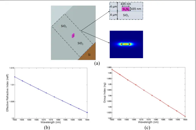
showing the cross-section waveguide geometry and TE mode distribution; (b) Wavelength dependent effective index (c) Wavelength dependent group index ... 34 Figure 3.4 (a) Perspective view of Si channel waveguide with insets showing
the cross-section waveguide geometry and TE mode distribution; (b) Wavelength dependent effective index; (c) Wavelength dependent group index ... 35
XVI
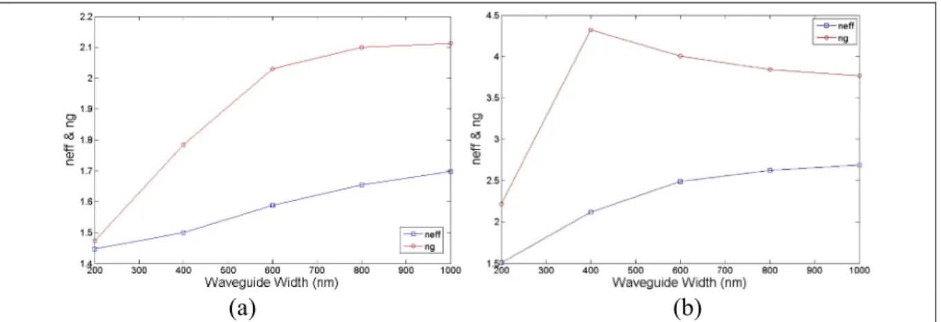
Figure 3.5 The effect of waveguide width variation over neff and ng at 1550 nm for (a) Silicon nitride waveguide (thickness of 435 nm), (b) Silicon
waveguide (thickness of 220 nm) ... 35 Figure 3.6 Symmetric and Antisymmetric modes dependence over the
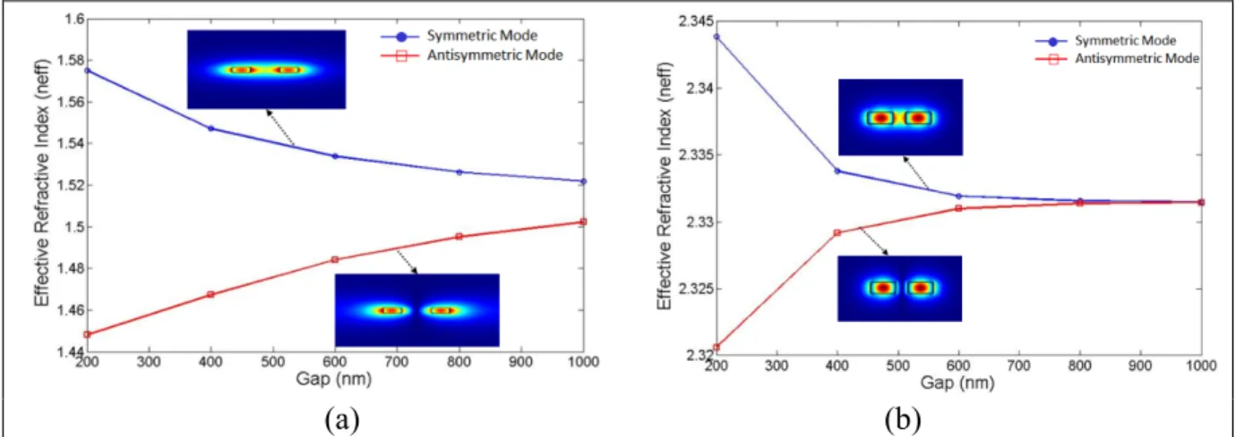
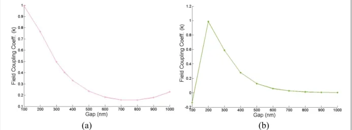
coupling gap at 1550 nm for (a) Si3N4 waveguide (b) Si waveguide;with insets showing supermodes electric field distribution ... 36 Figure 3.7 Field coupling coefficient ‘k’ versus coupling gap at 1550 nm for
(a) Silicon nitride waveguide having dimensions 435 nm x 435 nm (L=20 μm), and (b) Silicon waveguide having dimensions 440 nm
x 220 nm (L=20 μm) ... 36 Figure 3.8 General schematic of a single ring reflector based on Si3N4
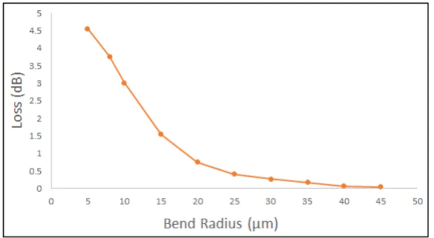
waveguide with dimensions 435 nm x 435 nm ... 38 Figure 3.9 Waveguide bend loss versus radius for 435 nm wide Si3N4
waveguide (in dB scale) ... 38 Figure 3.10 Effect of field coupling coefficient κ on the drop port peak intensity
of an add-drop ring resonator ... 39 Figure 3.11 (a) Simulated spectral response of a silicon nitride single ring
reflector, (b) zoom in of the resonance peak of the reflection/drop
port response ... 40 Figure 3.12 FSRs for three different ring reflectors, each of them showing a
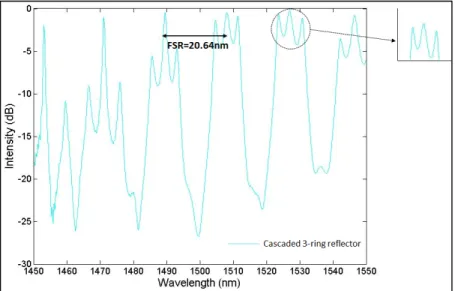
common central wavelength around ~1492 nm ... 42 Figure 3.13 The reflection response of a serially coupled 3-ring reflector in a
2.5D-FDTD showing resonance peak splitting ... 43 Figure 3.14 The effect of the coupling coefficient ‘κ’ on the drop port peak
intensity of Si waveguide based single ring resonator of radius (a)
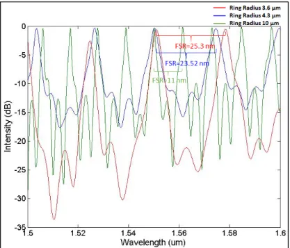
3.6 μm (b) 4.3 μm and (c) 10 μm ... 45 Figure 3.15 Reflection spectra obtained from 2.5D-FDTD for three different Si
ring reflectors showing their corresponding FSRs ... 46 Figure 3.16 Reflection spectra for a serially coupled Si 3-ring filter illustrating
the Vernier effect and showing the dominant resonant peak without
peak splitting ... 47 Figure 3.17 A generalised process flow for the fabrication of the Si3N4
XVII
Figure 3.18 Optical Test Measurement Setup (1) (a) Single mode input fibre (b) Single mode output fibre (2) Device chip (3) Chip holding stage (4) Chip stage controller (5) Three axis stage controller for (a) input
fibre (b) output fibre (6) Polarization rotator (7) Microscope ... 51 Figure 3.19 The through port transmission response for (a) Device 6, (b) Device
8 & (c) Device 9 ... 53 Figure 3.20 Comparison of the through port transmission response for 3 devices
... 55 Figure 3.21 (a) Theoretical vs Experimental through port response for devices
6, 8 and 9 (b) Zoomed in response of plot (a) ... 56 Figure 3.22 SEM image of the (a) fabricated waveguides forming the coupling
region and (b) the cross section of the waveguide ... 57 Figure 3.23 Normalized curve showing theoretical vs experimental response for
varying widths (a) Device 6 (435 nm) (b) Device 8 (445 nm) (c)
Device 9 (455 nm) ... 59 Figure 3.24 The effect on the neff of the fundamental TE and TM mode for the
(a) Fabricated waveguide width (386 μm top x 427 bottom) vs. the varying waveguide thickness and (b) Fabricated waveguide thickness of 453 μm vs. the varying waveguide width ... 60 Figure 4.1 (a) Electrical signal at the input, and a distorted (b) optical signal at
the output, of a DML due to chirp ... 64 Figure 4.2 Change of instantaneous frequency ωinst with time showing blue and
red shift ... 65 Figure 4.3 (a) Perspective view of a Si3N4 channel waveguide with insets
showing the cross-section waveguide geometry and fundamental TE & TM mode distribution; (b) Wavelength dependent effective index for TE mode (c) Wavelength dependent group index for TE mode (d) Wavelength dependent effective index for TM mode (e)
Wavelength dependent group index for TM mode ... 68 Figure 4.4 The fabrication tolerance showing the change in the neff of
fundamental TE and TM mode at 1550 nm due to (a) variation in the width (fixed thickness at 400 nm) (b) variation in the thickness
(fixed width at 400 nm) ... 68 Figure 4.5 Field coupling coefficient ‘κ’ vs gap, λ=1550 nm, coupler length
XVIII
waveguide, calculated using the waveguide mode solver with a 10
nm mesh size ... 69 Figure 4.6 The neff of symmetric and antisymmetric modes versus the coupling
gap, λ= 1550 nm, 400 nm x 400 nm Si3N4 waveguide. ... 70 Figure 4.7 Waveguide bend loss vs. radius for 400 nm wide SiN waveguide (in
dB scale), bend angle of 900 ... 71 Figure 4.8 The schematic design of two different racetrack resonators (a) Type
A, (b) Type B ... 72 Figure 4.9 Simulated optical response for type A racetrack-resonator... 73 Figure 4.10 Simulated optical response for type B racetrack-resonator ... 73 Figure 4.11 The intensity profile of the light propagating inside the racetrack
resonator obtained using 2.5D-FDTD simulations in Lumerical MODE ... 74 Figure 4.12 Transmission spectra for a small ring filter, waveguide 400 nm x
400 nm ... 76 Figure 4.13 SEM image of (a) the fabricated RR and (b) the coupling region of
RR showing variation in the gap and the waveguide widths. ... 77 Figure 4.14 Field coupling coefficient ‘κ’ vs gap, λ=1550 nm, coupler length
L=10 μm, L=15 μm, L=20 μm, L=25, L=30 μm and L=35 μm, 435 nm x 435 nm waveguide, calculated using the waveguide mode
solver with a 10 nm mesh size. ... 79 Figure 4.15 The general schematic design of a large racetrack resonator ... 80 Figure 4.16 Simulated optical spectra of a large racetrack resonator showing
transmission at the drop port and the through port (in dB) ... 81 Figure 4.17 A general schematic of the circuit simulation setup in the Lumerical
Interconnect showing 4 different configurations... 82 Figure 4.18 Plot showing ER (in dB scale) vs. detuning (Δλ) for configuration
(3) ... 83 Figure 4.19 Graph showing pulse amplitude from the laser (red line) and the
comparison of pulse amplitudes after the propagation through ring filter for lower ER (blue dashed line) and higher ER (black dashed
XIX
Figure 4.20 Power spectrum as a function of frequency (THz) showing adiabatic
chirp ... 84 Figure 4.21 Measured spectra showing the transmission at the through and the
drop port for a large racetrack resonator ... 85 Figure 4.22 SEM image of a directional coupler of a fabricated large RR ... 86 Figure 4.23 Normalized transmission spectra (in dB) showing the simulated and
LIST OF ABREVIATIONS AND ACRONYMS
2.5D 2.5 dimensional
2D Two dimensional
3D Three dimensional
BOX Buried oxide
CMC Certified management consultant CML Chirp managed laser
CMOS Complementary metal-oxide semiconductor CMT Coupled mode theory
DBR Distributed Bragg reflector
DC Directional coupler
DCM Dispersion-compensation module
DML Directly modulated laser
DRIE Dry-reactive ion-etching
DWDM Dense wavelength division multiplexing ECL External cavity laser
ECR-CVD Electron cyclotron resonance plasma enhanced chemical vapor deposition EM Electro-magnetic
EME Eigen mode expansion
EML Externally modulated lasers
ER Extinction ratio
XXII
FDE Finite difference element FDTD Finite difference time domain FP Fabrey-Perot FSR Free spectral range
FWHM Full width at half maximum GaInAsP Gallium indium arsenic phosphide Gbps Giga bits per second
GHz Giga Hertz
HMDS Hexamethyldisilazane
ICP Inductively coupled plasma
IME Institute of microelectronics
InP Indium phosphide
INRS National institute of scientific research IR Infra-red
ITU International telecommunication union LiNbO3 Lithium niobate
LPCVD Low pressure chemical vapor deposition LSCVD Liquid source chemical vapor deposition MDM Mode division multiplexing MEMS Micro-electro-mechanical-systems
MRR Micro ring-resonator
MZI Mach-Zhender interferometer
XXIII
OSA Optical spectrum analyser
OSR Optical spectrum reshaper
PDK Process design kit
PECVD Plasma enhanced chemical vapor deposition PMD Physical media dependent
PMMA Polymethyl methacrylate PON Passive optical network
RIE Reactive ion etching
RR Racetrack resonator
RR Ring-resonator
SHREC Silicon photonic hybrid ring-filter external cavity Si Silicon
Si3N4 Silicon nitride
SiN Silicon nitride
SiO2 Silicon dioxide
SiON Silicon oxynitride
SOI Silicon-on-insulator
TE Transverse electric
TM Transverse magnetic
TWDM Time and wavelength division multiplexing TWR Travelling wave resonators
XXIV
varFDTD Variational FDTD
WDM Wavelength division multiplexing
LIST OF SYMBOLS AND UNITS OF MEASUREMENT
kW Kilowatt
Gb/s Gigabit per second Km Kilometers GHz Giga Hertz THz Tera Hertz Λ Grating periods λr Resonant wavelength R Ring radius m Integer number
neff Effective refractive index of the waveguide ng Group index of the waveguide
n effective index of material C Coupling coefficient κ Field coupling coefficient π pi=3.14
n1 effective refractive index of symmetric mode n2 effective refractive index of antisymmetric mode Δn difference between symmetric and antisymmetric mode λ Wavelength
β1 Propagation constant of symmetric mode β2 Propagation constant of antisymmetric mode L Length of directional coupler
XXVI
Po Input optical power
Pcross Power coupled across the directional coupler t Transmission coefficient
Pthrough Power remaining in through waveguide Lx Cross-over length
Lc Coupling length g Gap
Et1 Through port waveguide mode amplitude Et2 Drop port waveguide mode amplitude α Loss coefficient of the ring
|t| Coupling losses of the ring φt Phase of the coupler θ Phase of the ring
Pt1 Modal power coming out of the through waveguide Pt2 Modal power coming out of the drop waveguide Pi2 Circulating power inside the ring
φ Phase difference variation in-between t and κ in both couplers of ring resonator Δλ Distance between the resonance peaks or FSR
2δλ 3-dB bandwidth EIN(z) Input node
ET(Z) Through port node ED(Z) Drop port node
XXVII
H Network function relating an input to an output port
Ti Gain (or transmittance) of the i-th forward path from an input to an output port. n Total number of ports.
Δi Determinant Q Quality factor
λ0 Central resonant wavelength dB Decibel mW Miliwatt oC Degree celcius mm Mili meters nm Nano meters μm Micro meter cm Centi meter dBm Decibel-milliwatts dB/cm Decibels per centimetre dB/m Decibels per meter m Meters
Qc Quality factor of the coupling between the microdisk and bus waveguide. (3 Third order non-linear susceptibility
pm Picometer
ωinst Instantaneous frequency Ith Threshold current
XXVIII
Symbols for Cascaded Ring Reflector
L1 Optical path length of racetrack-resonator 1 L2 Optical path length of racetrack-resonator 2 L3 Optical path length of racetrack-resonator 3
C1 Coupling region formed by bus waveguide and racetrack 1 C2 Coupling region formed by racetrack 1 and 2
C3 Coupling region formed by racetrack 2 and 3
C4 Coupling region formed by bus waveguide and racetrack 4 FSRextended Extended FSR obtained on cascading racetrack resonators m1 Resonant number and co-prime integer of ring 1
m2 Resonant number and co-prime integer of ring 2 m3 Resonant number and co-prime integer of ring 3
INTRODUCTION
With the increasing demand for high data transfer rates, there is a need for high performance networks that can maximise these transfer rates. Various optical components are being used to develop wavelength selective mechanisms for lasers and add-drop multiplexers in dense-wavelength-division-multiplexing (DWDM) optical communication systems. DWDM optical access networks allow the same spectral efficiency in the last mile as found in the core networks (Yoffe, Nguyen, Heanue, & Pezeshki, 2012). In order to achieve such high data transfer systems, the key technology is to implement tunable transceivers including compact, cost-effective and efficient tunable lasers and optical filters. These efficient and compact devices can come to a reality by using optical filters such as microring resonators and microdisk resonators which are already showing an unprecedented reduction in the footprint of optical devices.(Meindl, 2003)
As advancements in the microelectronic industry increases rapidly, complementary-metal-oxide-semiconductor (CMOS) compatible photonics tends to overpower the electronic communication system, since, the data transmission via optical fibres and optical waveguides system enhances the transmission range and the bandwidth of signals. The benefits of signal transmission through an optical waveguide are low power consumption, durability and very low transmission losses in comparison to the traditional electrical transmission lines. With silicon based integrated photonics, the bandwidths of orders of magnitude larger than the electronic networks are achievable. Wavelength-division-multiplexing (WDM) enables a single waveguide to carry multiple data streams. The CMOS compatible photonics allows to create complex optical devices at the chip scale. Ring-resonators are the prime examples of compact and high Q-factor filters being widely used in tunable lasers. With this vision, we present ring-resonator passive optical filters in Chapter 3 to be used as the reflector filters in the external cavity lasers (ECLs). These have a wide free spectral range (FSR) so as to cover the entire spectrum of the gain chip, thus, finding its utility in tunable laser applications.
2
The International Telecommunication Union (ITU) requirements for a passive optical network (PON) systems with a nominal aggregate capacity of 40 Gb/s in the downstream direction and 10 Gb/s in the upstream direction is referred to as the next generation passive optical network stage 2 (NGPON2). The ITU-T G.989.2 recommendation describes a network supporting multiple services with bandwidth requirements running at a downstream rate of 4 x 10 Gb/s. This recommendation based on time and wavelength division multiplexing (TWDM) was proposed to address the increasing bandwidth demand (Kazovsky, Shaw, Gutierrez, Cheng, & Wong, 2007). This advancement in the technology compels the development of novel 10 Gb/s-transmitters which necessitate innovative but also cost-effective and compact solutions providing long transmission range (>60 Km) and high extinction ratio. Chirp managed laser (CML) are systems using an external filter in front of a directly modulated laser (DML) to attenuate the inherent chirp of a laser by aligning the laser wavelength to the transmission edge of the filter. This allows to significantly increase the extinction ratio and the reach of the signals by attenuating the data bits ‘0’ and allowing only data bits ‘1’. Thus, in chapter 4, we discuss and demonstrate a Si3N4 waveguide based compact passive ring resonator, which can be used as an external filter aiding to increase the extinction ratio of tunable lasers. We present a cost-effective method to develop such a filter by using the traditional CMOS compatible fabrication process and its compactness allows the smaller footprint on the chip-scale integration as compared to other bulky etalon filters.
CHAPTER 1
SILICON PHOTONICS IN OPTICAL COMMUNICATIONS
In accordance with the more than Moore principle, several functionalities have been added at the chip scale, making them applicable in the diverse fields. The enormous amount of data storing computers and their associated components deployed within data centres consume large amount of electrical energy thereby increasing the operation cost. The future of computer technology rellies on ultra-fast data transfer rates between and within the microchips (Meindl, 2003). The speed of the top 500 supercomputers has increased exponentially during the last two decades, as shown in Figure 1.1, which is soon expected to reach the Exascale (1018 FLOPs) by year 2020. This increase in the speed is giving rise to huge bandwidth demands, which according to leading companies such as IBM and Intel, can only be met by investing
Figure 1.1 Performance of the top 500 supercomputers in the world
Taken from (https://www.nextplatform.com/2015/07/13/top-500-supercomputer-list-reflects-shifting-state-of-global-hpc-trends/)
4
heavily in the field of silicon photonics to provide much faster data transfer rates. Thus, silicon photonics helps in keeping on track with Moore’s Law.
A data centre with many servers incurs high opearational costs and power consumption due to increase of optical components on a small chip size. Thus, there is a tremendous need for developing highly efficient miniaturized optical components that could bring down the cost of high speed optical interconnects to 1$/Gbps. Resolving these challenges need the development of compact and efficient tunable transcievers which can be used in dense wavelength division multiplexing (DWDM) systems. These DWDM optical communication systems provides high performance networks which are able to meet with the high data transfer rates and provide the same spectral efficiency till the last mile (end users) as it is found in the core networks. High refractive index contrast waveguides, which can be implemented with the CMOS fabrication technology, have allowed the development of photonic circuitry using electronic fabrication facilities. This has made the silicon nitride/silicon photonics one of the most promising optical integration platforms over the last few years leading to the possibility of developing highly efficient miniaturized optical components and tunable lasers that could bring down the cost of optical interconnects.
1.1 Thesis Objective
The main objective of this thesis is to design, fabricate and characterize the silicon nitride (Si3N4) waveguide based integrated optical filter components with potential application for wavelength selective devices. A 3rd order Si3N4 ring filter in a reflector configuration will be designed to have a wide free spectral range (FSR), which can be used to develop a wavelength channel selection mechanism in a tunable external cavity laser (ECL). This small ring reflector will provide an optical feedback mechanism and allow the wavelength tuning of a laser. Also, a Si3N4 ring filter with an aim of developing an optical eye reshaper, will be designed having a large extinction ratio (ER) to be potentially used as a tunable transmitter in the NG-PON2 systems. This external ring filter having a FSR of 100 GHz, will be used in future along with the tunable laser to implement a CML. With this view, the optical components such as
micro-5 ring/racetrack resonators will be designed and optimized leading to the innovative transceivers application.
1.2 Methodology
The devices demonstrated in this thesis were fabricated using a CMOS compatible process. The research methodology is illustrated in Figure 1.2. The research methodology cycle begins with an idea emerging through the literature review, brain storming and workshops/conferences. The design model is based on the standard 8’ Si wafer covered with a 4 μm thick oxide layer. Later, simulations and optimization of basic building blocks such as directional couplers, Y-splitters, and waveguide bends, are done using analytical models, further leading to the design optimization of the final devices such as racetrack resonators with
6
the aid of the numerical tools such as Eigen-mode expansion (EME) and the finite difference time domain (FDTD) solvers. Afterwards, the photolithographic mask used for fabrication is designed. In order to build our devices, we have used the fab facilities of IME*Singapore accessed via CMC Microsystems (strictly following the PDK) and several other lab facilities of universities across Montreal, Canada such as INRS, Polytechnic and McGill. The recipes associated with the microfabrication steps such as dry reactive ion-etching (DRIE), e-beam lithography, low-pressure chemical vapour deposition (LPCVD) and plasma enhanced chemical vapour deposition (PECVD) were modified to obtain an optimized process flow in collaboration with the fellow researchers and the clean room personals. Through the efficient mix and match of the lithographic techniques, a large range of dimensional issues were addressed as and when required. After receiving the fabricated chips from the fabs, optical testing and measurements are performed in the UQAM lab facilities using an advanced alignment setup to investigate the propagation and insertion losses, followed by the transmitted/reflected spectrum analysis using an optical spectrum analyser. After this, the data processing and analysis is done by comparing the simulated and the experimental results, leading to the model verification and improvement. Eventually the results obtained are presented in conference presentation. The above methodology cycle was repeated in order to build each device and some fab-variations were carried out from time-to-time in order to resolve the structural discrepancies and to solve the challenges arising while testing of the optical devices.
1.3 Thesis Contributions
In this thesis, we present ring filters in different configurations, contributing to the field of silicon/silicon nitride photonics as follows:
1) Racetrack resonator filters for CML: We design and demonstrate a Si3N4 racetrack resonator, with a FSR in close proximity to the ITU channel grid, to be used as an external filter along with a tunable laser to implement chirp managed lasers (CML). 2) Ring reflector filter for tunable laser: We designed a 3rd order ring filter in a reflector
L-7 band. Also, we demonstrate a Si3N4 ring reflector, providing a novel approach towards future designing of a high order ring reflector (using Si3N4 waveguide), for the tunable laser application.
1.4 Thesis Organization
This thesis is organized as follows:
In Chapter 2, the state-of-the-art is presented for the silicon (Si)/silicon nitride (SiN) microring resonator and micro-disk resonator optical filters depicting its advantages over other passive filters with applications in optical transceivers. In Chapter 3, we present a novel silicon ring reflector, composed of three racetrack resonators (RRs) coupled in series, in order to have a wide FSR achieved by the Vernier effect. Also, a single ring reflector based on a silicon nitride waveguide is modeled and demonstrated. The design and modelling of a single and a cascaded ring-reflector is carried out using an analytical approach and the obtained simulated results investigate the important parameters such as the FSR, quality factor, bus-resonator coupling, ER and transverse modes. Moreover, the transmission and the reflection properties obtained from the experimental results for a silicon nitride waveguide based single ring reflector validates the characteristics mentioned above and also the structural discrepancy between the fabricated and simulated designs. Chapter 4 demonstrates two designs of the SiN waveguide-based racetrack resonators, to be used in CML. Design 1 is a 4-port add-drop racetrack resonator having an optical path length corresponding to a FSR of 718.75 GHz, whereas, design 2 comprises a large optical path length for a specific application in the next generation passive optical networks (NGPON2) systems. An analytical model, starting from the directional coupler and leading to the design approach of a fully optimized 4-port add-drop ring filter is presented. Important characteristics of RRs such as propagating modes, quality factor, ER, FSR and bus-resonator coupling are investigated in experimental and numerical simulations.
CHAPTER 2
PASSIVE OPTICAL FILTERS: A LITERATURE REVIEW
Complex photonic integrated circuits are usually constructed from various fundamental photonic building blocks or components. Fibre Bragg gratings were used early in wavelength filtering mechanisms because of their flexible filtering capability, low insertion and reflection losses and low cost. Fibre Bragg gratings were first presented by (Kawasaki, Hill, Johnson, & Fujii, 1978). Later Lam and Garside in 1981 showed that the refractive index modification was related to the square of the Argon laser intensity (Lam & Garside, 1981) in the experiments performed by (Kawasaki et al., 1978). The integration of waveguide Bragg gratings in the silicon-on-insulator (SOI) platform (G. Jiang et al., 2011; X. Wang et al., 2012) has been of great interest and its compatibility with the CMOS technology (X. Wang et al., 2012) has made it even more economically viable providing an ease of fabrication. Thus, they have found numerous applications in the area of optical communication (Vargas & Vazquez, 2014), such as WDM filters (Painchaud, Paquet, & Guy, 2007), single channel-extraction filter for dense wavelength division multiplexing (DWDM) applications (Alonso-Ramos et al., 2014), dispersion engineering (Cliche et al., 2007), lasers (Rochette, Guy, LaRochelle, Lauzon, & Trepanier, 1999), optical signal processing (Wang & Yao, 2013), wavelength selection mechanism and dispersion compensation (Giuntoni et al., 2010) and bio-sensing system (Jugessur, Dou, Aitchison, De La Rue, & Gnan, 2009). The issues with using Bragg gratings is that they require a large on-chip area and need an optical circulator to access the reflected Bragg wavelength signal which adds to the loss in power intensity of the signal. Depending upon the application, the number of grating periods (Λ) is selected to have an efficient optical filter. Each grating period has a length of hundreds of nanometres and depending upon application, the number of grating periods are chosen so as to have an optimum Bragg wavelength and the band rejection. This results in a large device footprint in the range of millimetres. When these large size filters have to be used in an active state such as in lasers and phase-shifted modulators, they need to be thermally or electrically tuned thereby increasing power consumption (as the whole grating or corrugated area needs to be actuated)
10
and fabrication cost. Therefore, with an increasing demand for optical filters in telecommunication applications, there is a tremendous need to make compact and economically viable optical devices in addition to maintaining the high quality factor and efficient wavelength filtering mechanism. This is provided by micro-ring resonator (MRR)/microdisk resonators which show a tremendous reduction in the footprint, better flexibility, less losses and minimal cost. Moreover, the wavelength tuning mechanism for the wavelength selection process will be electrostatic actuation which needs low power consumption. Thus, in this chapter, an extensive review of micro ring-resonator and micro-disk resonator filters is presented illustrating its applicability and leading edge over other filters.
2.1 Microring Resonators for Transceiver Applications
Passive silicon waveguide structures have shown an unprecedented reduction in the footprint of wavelength selective devices where microring resonator is a prime and interesting example of this. A microring is a circular waveguide excited by a bus waveguide where a fraction of input power from the bus waveguide couples into the ring. The most common coupling mechanism used is co-directional evanescent coupling between the ring and an adjacent bus waveguide. Resonance occurs within the ring cavity when the optical path length of the resonator is exactly a whole number of the wavelengths i.e. for the light whose phase change after each full trip around the ring is an integer multiple of 2π, which is of course the condition for the light in the ring to be in-phase with the incoming light from the bus and causes constructive interference. Light which does not meet this resonant condition is transmitted through the bus waveguide. The expression for the resonant wavelength is very similar to a Fabry-Perot (FP) cavity and is given by (Bogaerts et al., 2012):
= (2.1)
where, ‘R’ is the ring radius, ‘m’ is an integer and is the effective refractive index of the waveguide. In order to achieve an effective ring-resonator, the design of a proper coupling
11 region is required. In the case of a racetrack resonator, directional couplers (DC) should be studied and designed properly. A DC is the most common device to split and to combine light in a photonic system. A DC consists of two parallel waveguides where the field coupling coefficient ‘κ’ is controlled by the coupler gap i.e. the spacing between the two waveguides and the coupler length. At first, the coupling coefficient ‘C’ is determined using the supermodes analysis method, based on the numerical calculation of the effective indices n1 and
n2, of the first two eigenmodes of the coupled waveguides. These two modes are known as
symmetric and antisymmetric modes, also generally known as supermodes. The Eigen mode expansion method (EME) is an another method which is more accurate than the traditional coupled mode theory (CMT) method (Yariv, 2000) especially for the high-index contrast waveguides where the coupling coefficient is found using the perturbation methods. From these two supermodes, the ‘C’ can be written as (Chrostowski & Hochberg, 2015):
= (2.2)
where Δn is the difference between the effective indices, n1-n2, also known as birefringence.
The two modes propagating inside the waveguides have different propagation constants as given in (Chrostowski & Hochberg, 2015, p. 93):
= (2.3) = (2.4)
Then a fraction of the power coupled from one waveguide to another can be expressed as shown in (Chrostowski & Hochberg, 2015, p. 92):
κ2= = ( . ) (2.5)
where P0 is the input optical power, Pcross is the power coupled across the directional coupler,
12
power in the original ‘through’ waveguide (assuming a lossless coupler i.e. κ2 + t2 = 1) is given
by (Chrostowski & Hochberg, 2015, p. 92):
t2 = = ( . ) (2.6)
As the modes propagate, the field intensity oscillates between two waveguides as shown in Figure 2.1, where if the two modes are in phase then the power is localized in the first waveguide. After a π phase shift difference between the modes, the power becomes localized in the second waveguide which occurs after a distance known as the cross-over length ‘Lx’
which is shown in (Chrostowski & Hochberg, 2015, p. 93):
β1Lx – β2Lx = π
− =
= (2.7)
Figure 2.1 Field propagation along a directional coupler. Modes calculated using the waveguide mode solver and the modes are propagated using the eigenmode
Taken from Chrostowski & Hochberg (2015, p. 95)
The C has a dependence on the distance between the waveguide ‘g’ which follows an exponential behaviour given by (Chrostowski & Hochberg, 2015, p. 94):
13 where A and B are dependent on the geometry of the coupler, optical wavelength, etc. Thus the field coupling coefficient ‘κ’ can be found for a directional coupler of any length or a gap using equation (2.5) as shown in (Chrostowski & Hochberg, 2015, p. 95):
= / = sin . = sin . (2.9)
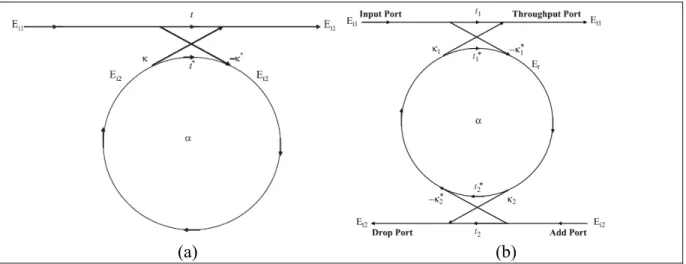
Thus, deciding an optimum value of field coupling coefficient ‘κ’ helps in determining the important parameters such as gap and coupling length for a directional coupler which is key in designing complex passive filters. Two types of ring filter configurations are shown in Figure 2.2, where the basic coupling model of a notch filter (Figure. 2.2(a)) and 4-port add-drop filter (Figure. 2.2(b)) is presented.
(a) (b)
Figure 2.2 Model of a (a) single ring resonator with one waveguide, which forms a ‘notch filter’ and (b) the basic add-drop ring resonator filter
Taken from Rabus (2007, p. 4-7)
For a notch type filter, the coupling between the bus waveguide and the ring is lossless and the various kinds of losses occurring along the propagation of the light in the ring resonator filter are incorporated in the attenuation constant. Then the interaction between the bus-waveguide and the ring can be described by the matrix relation given by (Rabus, 2007):
=
14
The complex mode amplitudes ‘E’ are normalized such that their squared magnitude corresponds to the modal power and the t and k are transmission and field coupling coefficients, respectively. The * denotes the complex conjugate of t and k. The matrix is symmetric since the device under consideration is reciprocal. Therefore,
| |+ | | = 1 (2.11)
and to further simplify the model, is chosen to be equal to 1. Then the round trip mode amplitude is given by (Rabus, 2007, p. 4):
= . (2.12)
where, α is the loss coefficient of the ring and θ = ωL/c (for further explanation, please refer to Appendix I). From (2.10) and (2.12), we obtain the other propagating mode amplitudes which are presented in (Rabus, 2007, p. 5):
= ∗. (2.13) = ∗ ∗ (2.14) = ∗∗ (2.15)
The corresponding circulating modal power inside the ring is then obtained by squaring the complex mode amplitudes (i.e. = | | and = | | ), which are derived in Appendix I. When the loss coefficient α = |t|, then the internal losses are equal to the coupling losses and the transmitted power becomes zero. This condition is known as critical coupling which is caused by destructive interference. When, α > |t| then the ring filter is said to be over-coupled and when α < |t|, it is considered to be under-coupled.
15 Now, when another bus-waveguide is included in the design to make it a 4-port add-drop filter (as shown in Fig. 2.2(b)), then the mode amplitude at the through port is given by (Rabus, 2007, p. 6):
= ∗ ∗∗ (2.16)
Now the mode amplitude has to pass through the second coupler as can be seen from the Fig. 2.2(b) so as to become the new dropped mode amplitude . The relation for the dropped mode amplitude in the second waveguide is given by relation presented in (Rabus, 2007, p. 6):
= ∗ / /
∗ ∗ (2.17)
where, α1/2 and θ1/2 are the half round trip loss and the phase given by α = / and θ = 2θ1/2.
At the resonance, the output power at the drop port is then given by the square of complex mode amplitude | |2 (shown in Appendix I). In the case of racetrack resonators, the coupling distance is approximately the length of the coupling sections. At a point where the curved and the straight waveguides combine, the mode changes adiabatically between the radial mode of the curved waveguide and the normal mode in the straight waveguide. Thus, in order to keep the total optical path length constant, the radius of the curved waveguides should be reduced if the waveguides are extended. It is important to consider the variation of the phase difference φ which occurs in the coupling region in both couplers between t and κ. The phase difference is length dependent and affects the output characteristics, not only in the magnitude but also in the resonant conditions. This phase difference can be introduced in equations 2.16 and 2.17 using the method described in (Lee et al., 2004) and the complete relation for mode amplitudes at the through port is then modified to (Rabus, 2007, p. 17):
= ∗ / ( ∗ ∗ ) ∗ ∗
16
and at the drop port it changes to (Rabus, 2007, p. 17):
= ∗ / /
∗ ∗ (2.19)
The resonant conditions for a racetrack resonator (θ + φt1 + φt2) = 2πm has changed slightly
compared to the ring resonator (θ + φt) = 2πm. The drop port transmission at resonance is no longer independent of t and κ. Thus, leading to a significant performance change and confirming the importance of taking into consideration the phase difference.
One important ring resonator parameter is the distance between the resonance peaks, which is called the free spectral range (FSR) and that can be described by (Rabus, 2007, p. 8):
= Δ = − ≈ (2.20)
If we include the wavelength dependency of the effective refractive index then the group index ng which is defined as = − , can be included in the equation (2.20). Then the
modified version of eqn. (2.20) given in (Rabus, 2007, p. 9) is:
= Δ = (2.21)
which can be used whenever appropriate to avoid the approximation and hence obtain more accurate values. Another important parameter is the width of the resonance which is defined as full width at half maximum (FWHM) or 3-dB bandwidth (2δλ) of the resonance lineshape. It is derived in Appendix I and is presented in (Rabus, 2007, p. 9) as:
17 Another parameter that can be directly calculated from the above relations is the finesse (F) of the ring resonator filter. It is defined as the ratio of the FSR to the width of a resonance for a specific wavelength (FWHM). This relation is given in (Rabus, 2007, p. 10) as follows:
= = = ≈ (2.23)
One more important parameter which is closely associated to the finesse is the quality factor (Q) of a resonator which is the measure of the sharpness of the resonant peak. It is defined as the ratio of the operation wavelength over the resonance width (Rabus, 2007, p. 10) as:
= = = (2.24)
For our design, we have specifically selected three racetrack resonators to be serially coupled in order to have a reflector configuration. The reflectors can only be designed by choosing the odd numbers of ring-resonators (such as n=1,3,5,7,…) such as the propagating light is reflected back to the input port. The coupling of these 3-racetrack resonators will help in achieving a broad FSR. The representation of the important functional parameters such as field coupling coefficient (κ), transmission coefficient (t) and the loss coefficient (α) within the ring can be seen in Figure 2.3. These parameters are kept the same while deriving the transfer equations for the output ports of the cascaded 3-ring filter. The input node is EIN (z), the through port
node is ET (z) and the drop port node is ED (z). Since there are three rings, there are four
coupling regions in the design. On the basis of the Mason’s rule (Mason, 1956), the transfer function or input-output transmittance relationship, having ‘n’ number of nodes (16 nodes depicted in Figure 2.3), from node E1(z) to node En(z) is given by (Chaichuay, Yupapin, & Saeung, 2009):
18
Where H is the network function relating an input to an output port, Ti is the gain (or
transmittance) of the i-th forward path from an input to an output port and n is the total number of forward paths from an input to an output port. Δi is the determinant Δ after all loops which
touch the Ti path at any node have been eliminated.
Figure 2.3 Model of a serially coupled three-ring add-drop filter showing the coupling coefficients and the loss coefficients for each ring
The forward path transmittances and its determinants from EIN to node ET and EIN to node ED
are shown in Appendix II, leading to the transfer function for the through port as follows (Chaichuay et al., 2009):
19
( )
( )= =
−1 −1 ( −1) −1 ( −1) ( −1) ( −1)
−1 −1 −1 ( −1) ( −1) ( −1) ( −1) (2.26)
Similarly, the transfer function for the drop port is given by (Chaichuay et al., 2009):
( )
( )= =
( )/
( ) ( ) ( ) ( ) (2.27)
In early years, before Si photonics became a path-breaking technology for integrated electro-optical systems, researchers mainly focused on III-V semiconductors and other glass materials. The first guided optical ring-resonator was demonstrated by (Weber & Ulrich, 1971) which was used for a laser application where they presented a device consisting of a 5-mm diameter glass rod (n=1.47) coated with a rhodamine 6G doped polyurethane film. This coated glass rod forms a ring like structure, placed in front of the pumping source, providing a positive feedback. The active medium is provided by the spiral resonator which has a circumference of 31.4 mm. The next relevant demonstration of a low-loss channel waveguides in a ring-resonator configuration was done by (Haavisto & Pajer, 1980) using a bus-waveguide made of a doped polymethyl methacrylate (PMMA) film on quartz substrate. Later, the first demonstration of tunable ring resonator on LiNbO3 with Ti diffused waveguides was made by (Tietgen, 1984) where they used two 3-dB couplers forming a waveguide loop instead of a circular ring. This loop has a circumference of 24 mm operating at 790 nm wavelength. The first ever electro-optically tuned GaInAsP-InP microring notch filter was reported by (Grover et al., 2004).
Over the past decades, microring resonators have been widely used for implementing a variety of wavelength-selective reflectors such as reflective notch filters (H. Sun, Chen, & Dalton, 2009) (Shi, Vafaei, Torres, Jaeger, & Chrostowski, 2010) (Chae & Skafidas, 2013) and reflective band-pass filters (Chung, Kim, & Dagli, 2006) (Paloczi, Scheuer, & Yariv, 2005) (Poon, Scheuer, & Yariv, 2004). These filters are very promising for applications such as remote sensing (Shi et al., 2010) (H. Sun et al., 2009), tunable lasers (Sato et al., 2015) (Tao
20
Chu, Fujioka, & Ishizaka, 2009), optical modulators (Xu, Schmidt, Pradhan, & Lipson, 2005), optical switches (Mokhtari & Baghban, 2015) and WDM add-drop filters (Van, 2007) (W. Wang et al., 2012) (De Heyn et al., 2013). Over the past two decades, tunable lasers have been successfully demonstrated on the Si platform since the optical filters made of Si waveguides provides well confined light propagation. These filters provide a feedback to the laser gain chip forming a lasing cavity. A general schematic of an external cavity semiconductor laser for wavelength tuning in telecommunications can be seen in Figure 2.4, where a feedback on one side of the semiconductor gain element is provided by an optical filter (blazed grating here). The DBR laser demonstrated by (Y. Liu et al., 2006) is one such example, which has many attractive performances and is now available for commercial use in optical network systems. However, for advanced multi-level modulation formats they are hard to use because of their wider linewidth resulting from their long cavity length.
Figure 2.4 A general schematic of an external cavity semiconductor laser.
This grating has been replaced by compact ring resonators in different configurations such as a SiON waveguide based serially coupled triple ring-resonator (Matsumoto et al., 2010) in a loop configuration, in a Littman configuration (Jeon et al., 2008), one with a phase shifter inside the cavity (Kita, Nemoto, & Yamada, 2014), another with two ring-resonators in series (R Boeck, Shi, Chrostowski, & Jaeger, 2013) (Ishizaka & Yamazaki, 2006), a polymer waveguide based single ring reflector using Y-splitters (Paloczi et al., 2005) and in a loop configuration with an asymmetric Mach-Zhender Interferometer (MZI) (Kita et al., 2014). Serially coupled two or three ring resonator filters uses the Vernier effect in order to achieve a wide FSR so as to cover the entire communication C-band. In these configuration, the lasing
21 wavelength corresponds to the simultaneously resonant component with the two/three ring resonators and is tuned by shifting the resonant wavelengths either by heating one, both (T Chu, Fujioka, Tokushima, Nakamura, & Ishizaka, 2010) (Ren et al., 2016) or all three ring resonators (Matsumoto et al., 2010). Other research groups have reported interesting configurations such as the combination of a microring with a contra directional-coupler (contra-DCs) (Robert Boeck, Caverley, Chrostowski, & Jaeger, 2015) and integrating a distributed Bragg reflector (DBR) inside the microring (Arbabi, Kang, Lu, Chow, & Goddard, 2011). This integration was done in order to eliminate the FSR so as to achieve low-threshold and narrow linewidth single mode laser diodes. This miniaturized half-ring DBR, shown in Figure 2.5, acts as a narrowband on-chip mirror which is way more attractive than conventional
Figure 2.5 a) Schematic of the ring with integrated DBR. The DBR is realized by modulating the top half of the ring waveguide. b) SEM image of the
fabricated device prior to top cladding deposition Taken from Arbabi et al. (2011)
DBR because of their small sizes and smooth narrowband high reflective peak at a single wavelength. In comparison to these configurations, where they have used a waveguide loop as a reflector within the optical coupling section, we present a novel serially coupled three ring filter in a reflector configuration where the 3rd order ring filter is integrated with the Y-splitters and combiners. Moreover, the tuning mechanism used in above mentioned configurations is thermal (using heaters) which sometimes produces excess heat thereby, degrading the device performance. In addition to this drawback, they have high power consumption due to thermal tuning which can be mitigated by adopting an electro-mechanical tuning. Therefore, with the vision of reducing the power consumption, the ring reflectors presented in this thesis will be tuned electro-mechanically using micro-electro-mechanical-systems (MEMS) in the future.
22
Another challenge with the silicon waveguide optical filters is the large propagation losses that degrade the transmission characteristics of the tunable ring resonators. The waveguide propagation losses reported by (Bogaerts et al., 2012) for silicon waveguides with air cladding in the IMEC foundry (Selvaraja et al., 2009) was around 2.7 dB/cm resulting in a Q-factor for an add-drop resonator of 1.36 x 10⁵ for a total length of 13 mm. This was drastically brought down to around 0.5 dB/cm by (Sato et al., 2015). They reported the best ever output power with more than 100 mW (20 dBm) at 250C for a silicon photonic hybrid ring-filter external cavity (SHREC) wavelength tunable laser. This power was high in comparison to the previous best reported by (Wakaba et al., 2013) of around 90 mW at 700C while achieving a wide tuning range of around 65 nm. The Si3N4 waveguide is less sensitive to fab dimensions and thus show low propagation losses as compared to the Si waveguide. Therefore, in this thesis, we demonstrate Si3N4 waveguide based ring-resonators to be used for different applications. A novel single ring reflector (similar to (Paloczi et al., 2005)) based on a Si3N4 waveguide and a Si 3rd order ring reflector design is presented in Chapter 3 with the goal to achieve a wide FSR with an aid of exploring the Vernier effect such that only a single channel lases within the gain bandwidth region. Thus, microring resonators are promising integrated filter components for developing compact external laser cavity allowing wide wavelength tuning range and high-Q factors at a low-cost for DWDM applications within the telecommunication bandwidth.
2.2 Microdisk Resonators for Transceiver Applications
Microdisk resonator is also a type of ring resonator, also known as travelling wave resonators (TWR), with a smaller internal radius of the inner ring (can be assumed as two concentric rings). The main advantage of TWRs over other optical filters such as Bragg gratings lies in the miniaturization of the devices. For a long time, it has been considered as a key opto-electronic filter with some of its modes giving a very high Q-factor (Levi et al., 1992). These modes, also known as whispering gallery modes (WGM), have light circulating around the circumference of the disk trapped by total internal reflection. In comparison to microrings, microdisks have smaller footprint, higher Q and wider FSRs which was shown by (Soltani, Li, Yegnanarayanan, & Adibi, 2010) by developing ultimate miniaturized microdisks and microdonuts (intermediate design between a disk and a ring shape). Microdisk have unique multi-modal and intrinsic
ultra-23 high Q properties (Soltani, Yegnanarayanan, & Adibi, 2007) due to which, careful coupling optimization is necessary to extract a single mode with the required Qc (quality factor of the coupling between the microdisk resonator and bus waveguide). The energy tail of the WGM of a microdisk decays more rapidly in the radial direction and outside the disk, as compared to a microring of the same radius. This leads to a weaker coupling of the microdisk to an adjacent waveguide, compared to the microring, thereby, making it difficult to achieve a critical coupling. If microdisks have larger radii then achieving the required Qc becomes more challenging, since the energy tail outside the disk approaches zero faster. A 100% energy transfer is possible from a bus waveguide to the resonator by an appropriate design of the waveguide-resonator coupling (Yariv, 2000). A few of the challenges faced when realizing such compact microdisk resonators are: firstly, the sidewall roughness induces scattering and absorption losses which can be reduced by developing improved fabrication techniques. Secondly, optimizing the waveguide-resonator coupling region to achieve critical coupling. These challenges were analysed by (Soltani et al., 2007) where they demonstrated a high Q~3x10⁶ Si microdisk resonator. They developed two device architectures for disk-on-substrate and assessed its integration with active components evidencing the useful role of the substrate for both chip-scale device integration as well as active electronic device integration.
In order to obtain a directional output, the rotational symmetry needs to be broken which can be done either by deforming the boundary which gives very low Q-factor (Gmachl et al., 1998), by inserting a linear defect (Apalkov & Raikh, 2004) or creating a hole (Wiersig & Hentschel, 2006) in a microdisk near the mode propagation region. For a microcavity with a thickness of only a fraction of mode wavelength, modes can be studied using a 2D approximation with the help of the effective refractive index n(x, y) = n(r, ϕ). In this approximation, the coordinate dependence of the EM field in the z-direction is omitted, resulting in the separated fields for the TM modes (Hz=0) and TE modes (Ez =0). For the TM modes the field is given by the relation (Dettmann, Morozov, Sieber, & Waalkens, 2008):
+ + + ( , ) = 0 (2.28)
24
= − (2.29) a) = (2.29) b)
For the TE modes with a new introduced function hz(r,ϕ) = Hz(r,ϕ)/n(r,ϕ), we obtain (Dettmann et al., 2008):
+ + + (r, ϕ)ℎ + ∇( , ) − 2 ( , ) ∇ ℎ = 0 (2.30)
with,
= ( , ) + ( , ) ( , )ℎ (2.31) a) = − ( , ) + ( , ) ( , )ℎ (2.31) b)
The relation for the effective refractive index and the field function (ψ) is derived and showed in Appendix III. Implementation of microdisks on a silicon platform has demonstrated a great potential for integration with other electronic and photonic devices. Among various micro-photonic components, microdisk resonators are being actively pursued for chip-scale silicon photonics (Srinivasan et al., 2005) (Borselli, Johnson, & Painter, 2005) (Johnson, Borselli, & Painter, 2006). Since, it is the most compact wavelength-selective reflector, it allows highly competitive tuning efficiency (in nm/W) for tunable lasers (Tao Chu et al., 2009). Due to their large tuning range and compact size they are promising for other applications such as sensing (Shi et al., 2012), optical routing switches (Emelett & Soref, 2005), stop-band filters (Morand et al., 2006), opto-mechanical oscillators (W. C. Jiang, Lu, Zhang, & Lin, 2012; X. Sun, Zhang, & Tang, 2012), force-gradient-actuated cavity opto-mechanics (X. Jiang, Lin, Rosenberg, Vahala, & Painter, 2009) (G. Li et al., 2015) and optical modulators (Zhou & Poon, 2006). These micro resonators have a very long photon life time and a strong electric field enhancement because of the small mode volumes and a high Q-factor that is achievable at such scale. This makes them a suitable candidate for the enhancement of light-matter interactions (Barclay, Srinivasan, Painter, Lev, & Mabuchi, 2006). These optical interconnects tends to revolutionize the computing technology with a minimal loss and high bandwidths.
25
2.3 Silicon nitride waveguide based Microring and Microdisk Resonators
Over the past decade, we have observed a tremendous development of photonic integrated circuits over silicon-on-insulator (SOI). The merits of using Si-photonics platform are large-area substrates, CMOS compatible high yield fabrication, availability of sophisticated assembly processes and enabling the manufacturing of densely integrated electro-optic components at low costs and high volumes (Soref, 2006) (Baehr-Jones et al., 2012) (Lim et al., 2014). Si-photonics is befitting for large complex photonic circuits, optical interconnect networks and optical switching networks, but, due to the losses, crosstalk and the fabrication tolerance of the conventional Si photonic platforms, its implementation is sometimes limited. Recently, low loss Si3N4 waveguide has been considered as a potential candidate for an integrated photonic platform. Its superior passive optical properties to Si (Henry, Kazarinov, Lee, Orlowsky, & Katz, 1987), a moderate refractive index (in-between oxide and Si) and low propagation losses in comparison to Si makes it a suitable material for realizing optical components for transceiver applications. Si3N4 has other advantages over Si such as it does not suffer from two photons and free carrier absorption over the telecommunication wavelength ranges which are preferred for parametric oscillation applications. Moreover, its third order non-linear susceptibility ( (3)) is about 20 times smaller than that of the silicon (Dinu, Quochi, & Garcia, 2003) (Ikeda, Saperstein, Alic, & Fainman, 2008). The lower index contrast of a silicon nitride (SiN, n≈2) to silica (SiO2, n≈1.45) compared to silicon (Si, n≈3.48) reduces waveguide losses due to sidewall roughness scattering. It is less sensitive to fabrication variations as compared to Si. Photonic components made of Si3N4 are also less temperature sensitive owing to a thermo-optic coefficient that is about five times smaller than that of Si (Amatya et al., 2007) (Cocorullo, Della Corte, & Rendina, 1999). Due to the above mentioned optical properties, many research groups are currently working and have recently demonstrated the integration of Si3N4 waveguides onto the SOI platform (Chen, Doerr, Buhl, Baeyens, & Aroca, 2011) (Jones et al., 2013) (Sodagar, Pourabolghasem, Eftekhar, & Adibi, 2014) and with hybrid III/V silicon platform (Piels, Bauters, Davenport, Heck, & Bowers, 2014), so as to combine active and passive optical functionalities in the Si-based integrated photonics.