HAL Id: hal-03039320
https://hal.archives-ouvertes.fr/hal-03039320
Submitted on 3 Dec 2020HAL is a multi-disciplinary open access
archive for the deposit and dissemination of sci-entific research documents, whether they are pub-lished or not. The documents may come from teaching and research institutions in France or abroad, or from public or private research centers.
L’archive ouverte pluridisciplinaire HAL, est destinée au dépôt et à la diffusion de documents scientifiques de niveau recherche, publiés ou non, émanant des établissements d’enseignement et de recherche français ou étrangers, des laboratoires publics ou privés.
Deposition Eu:Y 2 O 3 Thin Films through Optimized
Thermal Annealing
Marion Scarafagio, Alexandre Tallaire, Marie-Hélène Chavanne, Michel
Cassir, Armelle Ringuedé, Diana Serrano, Philippe Goldner, Alban Ferrier
To cite this version:
Marion Scarafagio, Alexandre Tallaire, Marie-Hélène Chavanne, Michel Cassir, Armelle Ringuedé, et al.. Improving the Luminescent Properties of Atomic Layer Deposition Eu:Y 2 O 3 Thin Films through Optimized Thermal Annealing. physica status solidi (a), Wiley, 2020, 217 (8), pp.1900909. �10.1002/pssa.201900909�. �hal-03039320�
1
Improving the luminescent properties of Atomic Layer Deposition
Eu:Y
2O
3thin films through optimized thermal annealing
Marion Scarafagio1, Alexandre Tallaire1, Marie-Hélène Chavanne1, M. Cassir 1, A. Ringuedé 1, Diana Serrano 1, Philippe Goldner 1 and Alban Ferrier 1,2*
1 Institut de Recherche de Chimie Paris (IRCP), Université PSL, Chimie ParisTech, CNRS, 75005 Paris, France
2 Sorbonne Universités, Faculté des Sciences et Ingénierie, UFR 933, 75005 Paris, France
E-mail: [email protected]
Keywords: Atomic layer deposition, sesquioxide, photoluminescence , lanthanide , quantum technologies
Crystalline rare-earth (RE) doped Y2O3 films are an attractive system for a wide range of
photonics applications including quantum technologies which aim at harnessing optical or spin
transitions with long coherence times to achieve new functionalities like quantum storage or
information processing. Here we present Atomic Layer Deposition (ALD) of Eu doped Y2O3
thin films with improved optical properties. A crucial post-treatment step to obtain high quality
films is annealing at elevated temperatures (> 900 °C). However the main drawback of this
approach is the formation of unwanted parasitic phases due to reaction at the interface with the
substrate, especially with silicon. In this paper, we discuss this issue for different kinds of
substrates and buffer layers. The use of such modified substrates allows advantageously
extending the maximum thermal treatment up to 1150 °C without being limited by interface
reactions. We demonstrate that emission of the 5D0 7F2 transition for Eu3+ in Y2O3 film can
be as narrow as that of bulk materials when optimized thermal treatments and a thin undoped
Y2O3 buffer layer are used. We thus propose a versatile method in order to reduce the impact
of the substrate-film reaction on the optical properties.
1. Introduction
The development of low cost, compact, highly integrated optical devices will greatly
benefit a large range of applications including optical sensing, telecommunication,
2
thin films appear as promising systems along other solid-state materials such as NV centres in
diamond or quantum dot semiconductors. Indeed promising results have already been obtained
on bulk single crystals as well as on nanoparticles.[1-6] Extremely long spin coherence times
(6 h) have for example been measured at cryogenic temperatures with Er:Y2SiO5 bulk crystals[7]
as well as all optical spin coherent control in Eu:Y2O3 nanoparticles.Thin film technologies, on
the other hand, are less explored although they could potentially open the way for on-chip
integration with other devices such as light sources or detectors. [8-9] To achieve that, a key
requirement is the growth of thin crystalline films of rare-earth-doped oxides with low levels
of impurities and defects. Besides, the development of high-quality films can also benefit a
broader community since new applications of Y2O3 have recently emerged such as catalyst for
biodiesel production, wastewater treatment, or anti-corrosion. [10--12]
Atomic Layer Deposition (ALD) enables the deposition of luminescent films with a
precise control of thickness at the atomic level. This method relies on exposing the substrate
surface alternately to different vaporized precursors until surface self-limiting regime is reached
(i.e. an almost complete monolayer of reactant is fully adsorbed at the surface). Thanks to that
sequential approach, ALD allows unique uniform and conformal deposition as well as dopant
distribution engineering that prevents concentration quenching even for relatively large doping
contents. [13-15] One of the inherent drawbacks of this technique though is the low growth rates
associated with this sequential layer-by-layer growth mode together with low deposition
temperatures required to remain within this self-limiting regime (e.g. 50°C - 400°C). [16-17]
Recently, we demonstrated for RE:Y2O3 10 nm-thin films that a high deposition
temperature and post treatment annealing above 900°C are key parameters for optimizing the
luminescent properties. In fact, by improving the crystalline environment of the ions, narrow
inhomogeneous lines were obtained for the 7F
0 ↔ 5D0 transition of Eu3+ even for nanoscale
films .[18] Other motivations to work with the cubic structure of Y2O3 are the isotropic refractive
3
nanomaterials. [5,6] However some limitations exist. On the one hand, deposition temperature
cannot be increased easily since it must remain within the ALD temperature windows where
the deposition process is surface limited (temperature range of 250–375 °C for Y(tmhd)3 and
O3 precursors). On the other hand the annealing post treatment temperature can only be
increased until about 950 °C on silicon above which parasitic silicate phases are formed and
modify the emission properties of the RE ions. [18]
In this work, we present strategies in order to further improve the optical properties of
thin Eu:Y2O3 ALD films and go beyond those limits. First, we investigated the deposition on
alternative refractory transparent oxide substrates such as sapphire (Al2O3) and yttria (Y2O3)
transparent ceramics in an attempt to further extend the post-treatment temperature. Another
approach is based on the use of buffer layers between the silicon and the luminescent layer. The
main idea is to space the reactive interface of silicon from the active RE:Y2O3 layer. We tested
two different buffer layers: Si3N4 or in situ grown undoped Y2O3. This approach aims at
developing devices compatible with silicon-integrated photonics. [18]
2. Results
Rare Earth sesquioxides are polymorphic materials with at least 5 different
crystallographic structures.[19] In the case of Y2O3, two main crystal structures are found: a
monoclinic (space group C2/m) and a cubic (Ia-3) one.[19,20] Unlike bulk crystals for which the
cubic structure is predominant, some competition occurs for nanoscale materials and a
monoclinic contribution may be detected. In a previous study, we indeed observed that both
phases are deposited by ALD on silicon. [18] The selection during the nucleation between the
cubic or the monoclinic structure is complex to predict since it is connected to deposition
parameters (temperature, pressure) and to the interaction between the surface and the yttria
nuclei. Indeed a correlation between the surface energy and the polymorphism have been
4
nature of the surface since the growth is surface self-limited. Modification of the orientation or
the nature of the substrate could lead to texture or new phase crystallisation in comparison to
silicon. In order to probe the effect of the substrate on the crystalline environment we used XRD
and photoluminescence (PL) of europium ion transitions. In particular, the 5D
0 7F2 emission
is used as a structural probe in order to distinguish the cubic from the monoclinic phase. Indeed,
a narrow line centred at 611 nm is expected for the cubic one whereas PL is broader and
redshifted for the monoclinic structure (centred around 625 nm). [22-24] This large variation is
observed because the forced electric dipole (ED) transition 5D0 7F2 is hypersensitive (J=2).
Those hypersensitive transitions are excellent environment probe since their intensities are
much more influenced by the local symmetry around the RE3+ ion than the intensities of the
other ED transitions. [25, 26]
2.1. Deposition on sapphire substrates
The main advantages of sapphire in comparison to silicon are the chemical
compatibilities for oxide films (e.g insensitive to oxidation), the transparency and the lower
refractive index (1.77 for sapphire against 1.89 for Y2O3 at 600 nm) useful for waveguide
technology.[27-28] Furthermore the higher melting point and thermal stability of sapphire in
comparison to silicon implies a lower reactivity. The main drawback in comparison to silicon
is the larger lattice mismatch with Y2O3 around 5 % (2 % on Si) but a lower thermal mismatch
is expected since the thermal expansion of Y2O3 and Al2O3 are closed. [29] Among the different
Al2O3 orientations, we selected the a-plane (11-20) since it shows cubic symmetry and can be
commercially obtained easily.
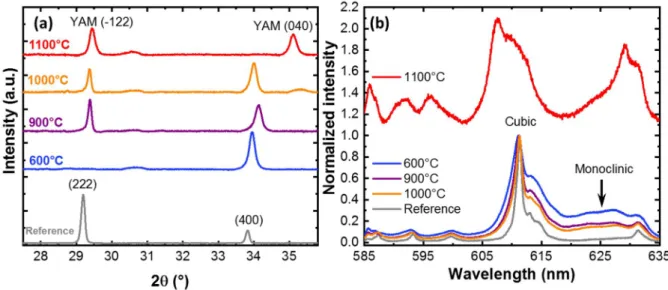
Figure 1a presents the XRD pattern of 87 nm-thick films doped with 5 % Eu3+ and
grown on a-plane sapphire for different post-annealing temperatures. The position of the 2 main
diffraction peaks: (222) and (400) are indicated. For as-grown and low annealing temperatures
5
[18] When the annealing temperature is increased, crystallinity improves and a change in texture
occurs since a significant contribution of the (222) planes appears. Other groups have already
observed similar changes in orientation during the post-annealing treatment. [28, 31, 32] Until
1000°C no additional phases are observed on the XRD pattern. At 1100 °C, the XRD pattern
changes significantly and new broad lines become visible, in particular at 29° and 35°. Those
new lines are attributed to the monoclinic yttrium aluminate (YAM) Y4Al2O9 (JCPDS card
00-034-0368).[33] This indicates that the deposited yttria layer has reacted by solid-state reaction
with the substrate at this temperature and that the ions are located in a different crystalline
environment. This solid-state reaction has already been reported for Y2O3 sol gel film deposited
on sapphire. [34]
Figure 1. Effect of the annealing temperature on the XRD pattern (a) and on the normalized room-temperature PL emission spectra of the 5D0 7F2 transitions (b) of 87-nm-thick Y2O3
films doped with 5 % Eu3+ and deposited on a-plane Al2O3 (11-20) substrates. The XRD data
in (a) are scaled to facilitate comparison. The Y4Al2O9 (YAM) peaks present a good agreement
with the JCPDS 00-034-0368. The PL spectrum of the sample annealed at 1100°C (in red) has been vertically translated for better clarity. Nanoparticles and a ceramic with the same composition are respectively used as a reference for the XRD pattern and the PL spectra.
The PL spectra presented in Figure 1b confirms this analysis. In a similar fashion to films
on Si substrates, a narrowing of the PL peaks is observed when the annealing temperature is
6
Furthermore emission arising from the monoclinic phase of yttria (indicated by an arrow in
Figure 1b) is reduced with an increase of the annealing temperature. When the temperature
reached 1100 °C however, the FWHM increased significantly indicating solid-state reaction
with the substrate. A blue shift of the main emission line from 611 to 607 nm suggests the
formation of a yttrium-aluminium mixed phase such as Eu:YAM .[35] In this phase, Eu3+ ions
substitute Y3+ ions located in a different C1 symmetry site. This multiplication of substitutional
sites together with the lowering of crystal symmetry can be responsible for the broadening of
the line observed in PL. [36] Therefore, although the use of sapphire as a substrate for Eu:Y2O3
thin film growth allows slightly increasing the maximum annealing temperature as compared
to a standard Si substrate, a limitation also exists at about 1100 °C due to the formation of
parasitic phases.
2.2. Deposition on Y2O3 transparent ceramics
Undoped Y2O3 transparent ceramics have been selected since, due to their having the
same composition as the layer, the absence of lattice and thermal mismatch, they may allow
limiting stress and interface reactions. The main drawback of this substrate is its
non-commercial availability and difficult preparation. [37] The substrates were cut into small pieces
of typically 5×5 mm² and mirror-polished. Structural analysis by XRD is difficult because of
the predominant signal from the substrate that cannot be easily distinguished from that
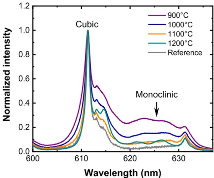
originating from the layer. For this reason, only PL results are presented. In Figure 2 the
5D
0 7F2 PL for different annealing temperatures are shown. For 900°C annealing and below
an important contribution from the monoclinic phase (indicated by an arrow) is visible showing
again that crystallinity remains relatively poor when low annealing temperatures are used.
When the annealing temperature is raised above 900 °C, a significant narrowing of the main
line at 611 nm is observed. Simultaneously disappearance of the monoclinic contribution occurs.
7
obviously no limitation in parasitic phase unlike other substrates considered previously. At the
highest temperature, the PL spectrum is very narrow and the different transitions between stark
sublevels at 622 and 627 nm are resolved. Therefore the use of such substrates seems to present
no real limits in terms of maximum annealing temperatures due to the absence of interfacial
reactions. However one has to take into account that diffusion of ions into the bulk ceramic
might occur for higher temperatures and longer annealing times. [38] This can possibly be a
limiting factor for the foreseen application in QTs for which spatial localization of the emitters
in a thin layer at the surface may be required. [39]
Although the transparent ceramic proves to be an ideal candidate for obtaining optimized
PL properties of ions in a very high crystalline quality environment, the difficulty of preparation
and poor availability of the substrates led us to turn to other strategies. In particular, silicon
remains an attractive platform with easier scaling-up and post-processing capabilities. The
possibility to limit surface reactions through the intercalation of a buffer layer was thus
attempted. 600 610 620 630 0.0 0.2 0.4 0.6 0.8 1.0 1.2 Normalized intensity Wavelength (nm) 900°C 1000°C 1100°C 1200°C Reference Cubic Monoclinic
Figure 2. Effect of the annealing temperature on the room-temperature PL emission spectra of 82-nm-thick Y2O3 films doped with 5 % Eu3+ and deposited on an undoped Y2O3 transparent
8
2.3. Deposition on silicon with a 100 nm-thick Si3N4 buffer layer
The first buffer layer studied is a 100 nm-thick low stress Si3N4 deposited on silicon by
PECVD (purchased from University Wafer). Deposition of Eu:Y2O3 luminescent films have
already been reported on Si3N4 membrane by e-beam evaporation. Furthermore, Si3N4 is a
particularly attractive option for capping passivation or buffer layer due to its high barrier
properties, low porosity and high chemical resistance. [40,41] Reactivity between silicon nitride
and Y2O3 have been largely reviewed since yttria is used as sintering additive of Si3N4 ceramics.
[42-44] During the high temperature sintering process, an intergranular crystalline secondary
phase of yttrium silicate like -Y2Si2O7 was shown to appear at the grain interface of -Si3N4.
[42-44]
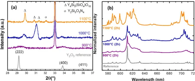
The XRD pattern and PL spectra are presented in Figure 3 for different annealing
temperatures. The XRD pattern for the 900°C annealing presents broad and weak peaks
indicating a poor crystalline quality. Furthermore, ratio of the (222) peak area on the (400) one
presents a value of about 2 whereas the expected ratio is about 3.6 for random orientation. The
use of Si3N4 buffer layer gives a polycrystalline film weakly textured and crystallized. From
1000°C, a significant change in the XRD pattern occurred and new lines appeared. Indexation
of these new lines suggested the presence of two yttrium silicate phases indicating a solid-state
reaction between the silicon substrate, the buffer and the Y2O3 layer.
The PL spectra confirms the XRD analysis. Indeed for a 900°C annealing post treatment
the characteristic PL of europium in the cubic and in the monoclinic phase are both present.
When the post treatment-annealing rose up to 1000°C a significant change in the PL spectrum
was observed, in a similar way as for a bare silicon wafer, indicating that a reaction occurred
between the oxide and the buffer layer or substrate. Therefore, the use of a Si3N4 buffer was not
9
Figure 3. Effect of the annealing temperature on the XRD pattern a) and the room-temperature PL emission spectra (b) of 100-nm-thick Y2O3 films doped with 5% Eu3+ and deposited on a Si
(100) substrate with a 100 nm buffer layer of Si3N4. Nanoparticles and a ceramic with the same
composition are respectively used as a reference for the XRD pattern and the PL spectra. The data are scaled to facilitate comparison. Indexation of the diffraction pattern have been done using the JCPDS 04-015-5862 for Y4Si3(SiO4)O10 and 01-086-1105 for Y2Si3O3N4.
2.4. Deposition on silicon with an undoped Y2O3 buffer layer
In order to move away the reactive interface between the substrate and the luminescent
layer, we interspaced a Y2O3 undoped layer. This 20 nm-thick buffer layer was deposited in
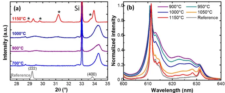
situ by ALD before the active luminescent layer of Eu:Y2O3. XRD pattern for different
annealing temperatures is presented in Figure 4. As already observed for deposition on silicon
a strong texture along the <100> directions is observed.[18] This texture remains whatever the
annealing temperature in contrast to growth on sapphire. Furthermore, we observed that the
diffraction peaks are shifted towards higher angles with respect to the reference which suggests
the presence of strain as already described in ref [18]. At 1000°C a careful analysis of the XRD
pattern revealed small additional peaks due to the formation of yttrium silicate compounds.
Those new silicate phases (such as Y2SiO5 and Y2Si2O7) are due to chemical reaction between
the Y2O3 film and the silicon wafer. For 1150°C annealing temperature, the intensity of the
XRD peaks of the silicate phase increased significantly and are indicated by a star on Figure 4a.
On the contrary, no additional lines were observed on the PL spectrum (Figure 4b) even for
10
emission of RE ions would start to be modified at temperatures as low as 1000 °C. In addition,
the Stark sub-levels were resolved for the highest annealing temperatures. This result indicates
that the silicate parasitic phase is well localized at the interface between the silicon wafer and
the undoped Y2O3 buffer layer but does not extend to the top Eu-doped layer in which the
optical properties of the ions are preserved. In this case the maximum temperature could be
increased to values as high as 1150 °C leading to a significant improvement of the crystalline
environment.
Figure 4. Effect of the annealing temperature on the XRD pattern (a) and room-temperature PL emission spectra (b) of Y2O3 films doped with 5 % Eu3+ and deposited on a Si (100) substrate
with a 20 nm-thick buffer layer of undoped Y2O3. Nanoparticles and a ceramic with the same
composition are respectively used as a reference for the XRD pattern and the PL spectra. Stars indicate the new XRD peaks due to the formation of silicate phase.
3. Discussion
Figure 5 and Figure 6 summarize the effect of the annealing temperature on the PL intensity
and area of the 5D
0 7F2 transition for deposition on different substrates. To better visualize
the effect we normalized the data with those collected for a 900°C annealing. The results are
presented up to temperatures at which parasitic phases appear. We can appreciate that the
annealing temperature has two effects. For low temperature annealing (less than 900°C) a
11
to 8. We attribute this larger emission to an increase of the number of Eu3+ ions that participate
to the PL spectrum. Indeed in this temperature window, the post treatment annealing is expected
to remove quenching centres that would otherwise limit total luminescence emission. This
hypothesis has been confirmed for deposition on silicon for which a substantial change in the
decay time is observed (not presented here). Indeed, for as grown or low-temperature annealed
films, the decay time presents a short lifetime with a non-exponential behaviour indicating a
strong quenching of the europium emission or energy transfer, whereas at higher annealing
temperatures the decay time approaches that measured for bulk crystals. [18] It is remarkable
though on Figure 5b that the PL area remains rather constant when the annealing temperature
is further increased. In contrast, the maximum PL intensity continues to rise (Fig 5a). This
suggests that crystalline quality improves and that, although the total number of ions
contributing to luminescence remains constant, their emission falls within a smaller
inhomogeneously broadened line. This is particularly striking for the highest annealing
12 300 400 500 600 700 800 900 1000 1100 1200 0 20 40 60 80 100 120 140
Peak intensity Normalized (%)
Silicon Al2O3 Y2O3 buffer PL Area Normalized (%) Annealing temperature 300 400 500 600 700 800 900 1000 1100 1200 0 40 80 120 160 200 240 Silicon Al2O3 Y2O3 buffer
Figure 5. Comparison of the 5D0 7F2 PL for films deposited on silicon, on Al2O3 (11-20) and
silicon with a 20 nm thick Y2O3 buffer layer. (a) Comparison of the variation of the normalized
integrated PL signal in the range 580-640 nm as a function of the annealing temperature. (b) Variation of the normalized 611 nm peak intensity for different annealing temperature. For each substrate the value of the PL area and PL peak intensity were normalized to that obtained for a 900°C annealing.
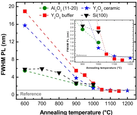
The results are finally summarized in Figure 6 which compares the FWHM of the main PL
emission at 611 nm for films grown on different substrates. We observe that it strongly
decreases with increasing the annealing temperature until the maximum temperature of
formation of parasitic phases (silicate or aluminate) is reached. Both depositions on the Y2O3
buffered substrate and the transparent ceramic allow advantageously extending the post
treatment to more than 1100 °C without encountering this issue. This translates into much
narrower PL linewidths that are comparable or even improved with respect to the reference bulk
13 600 700 800 900 1000 1100 1200 0 4 8 12 16 20 900 1000 1100 1200 0.8 1.0 1.2 1.4 1.6 1.8 2.0 2.2 2.4 2.6 2.8 3.0 F W H M P L ( n m ) Annealing temperature (°C) Reference FWHM P L (nm) Annealing temperature (°C) Al 2O3 (11-20) Y2O3 ceramic Y2O3 buffer Si(100) Reference
Figure 6. Comparison of the FWHM of the 5D0 7F2 red emission of Eu:Y2O3 as a function
of the annealing temperature. A drastic decrease in the FWHM is observed when the annealing temperature is increased. The inset represents a zoom into the high temperature area (850°C-1250°C). The reference value is measured on a transparent ceramic of the same composition.
4. Conclusion
In this work we fabricated Eu3+ doped Y2O3 thin films on different substrates by ALD and
compared the structural and photoluminescence properties with standard deposition on Si (100).
For all the substrates, crystalline films were obtained exemplifying the great versatility of the
ALD deposition technique. In order to maximize the PL intensity, a high temperature annealing
post treatment enhancement is required but the appearance of parasitic interfacial phases is
usually a strongly limiting factor. For growth on Al2O3 substrates, the maximum annealing
temperature is slight improved (1050°C) as compared to that of bare silicon (950°C).
Furthermore, the use of a buffer layer like Si3N4 did not help in increasing this temperature.
When a transparent ceramic is used as a substrate, no interfacial reactions are formed allowing
extending post-treatment up to 1200 °C. We note though that diffusion of the dopants deep into
14
are needed. Given the difficulty of preparation and poor availability of the material, transparent
Y2O3 ceramics also do not constitute an ideal platform. The use of a thin undoped Y2O3 buffer
layer was found to be the most appealing strategy allowing annealing up to 1150°C without
modifying Eu3+ photoluminescence whereas significant changes in the XRD pattern were
observed. This suggests that this thin layer acted as a sacrificial interface that reacted with the
silicon substrate and prevented the development of the silicate parasitic phase further into the
active Eu-doped film. The use of this approach of sacrificial undoped layer is a versatile method
that can be applied to other photonics systems.
5. Experimental Section
Film depositions were carried out with a a Picosun Sunale R200 using conventional
β-diketonate precursors: Y(tmhd)3 and Eu(tmhd)3 from (99.9% Strem Chemicals). These stable
precursors were held at 140-160 °C and delivered using 300 sccm N2 carrier gas. The vaporized
precursors were sent sequentially with an oxidant gas (O3) into the thermalized deposition
chamber at 300-350 °C. In order to maximize the film crystallinity, we used ozone as a strong
oxidizing agent. A typical ALD sequence consisted of a 3 s Y(tmhd)3 pulse followed by a 3 s
purging pulse of N2; a 3 s ozone pulse also followed by a 3 s purge with N2. Eu doping of the
oxide films was easily tuned by sequentially introducing pulses of the dopant element in the
standard yttrium oxide cycle. In our case, a doping level of 5 % was employed by introducing
5 pulses of Eu(tmhd)3 every 95 pulses of Y(tmhd)3. More details about the impact of the
different deposition parameters and their optimization are discussed in details in Scarafagio et
al. [18]
The following different substrates were considered for deposition: silicon (100), a-plane
Al2O3 sapphire (11-20), Y2O3 transparent ceramic and low thermal stress 100 nm-thick Si3N4
deposited on Si(100). All substrates were used as received after a cleaning with ethanol, acetone
15
ceramics that were provided by Dr Ikesue (World Lab Co, Nagoya, Japan). In order to remove
experimental bias, deposition on a reference silicon (100) wafer was done for systematic
comparison for each experiment. In order to improve the crystallinity of the films and the optical
properties of the emitters, we investigated a post-growth annealing treatment at different
temperatures under air for 2 hours. The crystallinity of the films was evaluated using X-ray
Diffraction (XRD) with a Panalytical XPert Pro diffractometer using an incident beam Ge
monochromator, and a stainless-steel sample holder. For all XRD patterns, baseline from
Fullprof free software was subtracted.
Film thickness was measured by white light interferometry in the range 250-1000 nm
with an Ocean Optics NanoCalc system using Y2O3 optical constants. Finally,
photoluminescence (PL) measurements were performed in a Renishaw InVia micro-PL
apparatus with a 50 × objective and a 532 nm laser as the excitation source.
Acknowledgements
This project has received funding from the European Union’s Horizon 2020 research and innovation program under grant agreement No 712721 (NanOQTech) and from Région Ile de France through the SIRTEQ framework. Dr Ikesue is thanked for providing transparent ceramic samples.
Received: ((will be filled in by the editorial staff)) Revised: ((will be filled in by the editorial staff)) Published online: ((will be filled in by the editorial staff))
References
[1] Goldner, P.; Ferrier A.; Guillot-Noël, O. Handbook on the Physics and Chemistry
of Rare Earths, 2015, 46, 1-78.
[2] Bussières, F.; Clausen, C.; Tiranov, A.; Korzh, B.; Verma, V. B.; Nam, S. W.;
Marsili, F.; Ferrier, A.; Goldner, P.; Herrmann, H.; Silberhorn, C.; Sohler, W.;
16
[3] Perrot, A.; Goldner, P.; Giaume, D.; Lovrić, M.; Andriamiadamanana, C.;
Gonçalves, R. R.; Ferrier, Phys. Rev. Lett., 2013, 111, 203601.
[4] Bartholomew, J. G.; de Oliveira Lima, K.; Ferrier, A.; Goldner, P. Nano Lett., 2017,
17, 778-787.
[5] Liu, S.; Serrano, D.; Fossati, A.; Tallaire, A.; Ferrier, A.; Goldner, P. RSC Adv. 2018,
8, 37098
[6] Serrano, D.; Karlsson, J.; Fossati, A.; Ferrier, A.; Goldner, P. Nat. Commun. 2018,
9, 2127.
[7] Zhong, M.; Hedges, M. P.; Ahlefeldt, R. L.; Bartholomew, J. G.; Beavan, S. E.;
Wittig, S. M.; Longdell, J. J.; Sellars, M. Nature 2015, 517, 177-181
[8] Tielrooij, K. J.; Orona, L.; Ferrier, A.; Badioli, M.; Navickaite, G.; Coop, S.; Nanot,
S.; Kalinic, B.; Cesca, T.; Gaudreau, L. et al. Nat. Phys. 2015, 11, 281.
[9] JH Kang et al. Opt. Express 2017 25 19561
[10] Pingbo Zhang Catal. Lett. 2019 149 2433–2443,
[11] S. Lee, et al. Thin Solid Films 2019 689 137455,
[12] Azimi, G.; Dhiman, R.; Kwon, H.-M.; Paxson A. T.; Varanasi, K. K. Nat. Mater.,
2013, 12, 315-320.
[13] J. Rönn, L. KArvonen, C. Kauppinen, A. Pyymaki Perros, N. Peyghambarian, H.
Lipsanen, A. Saynatjoki and Z. Sun ACS Photonics 2016 3 2040
[14] Proslier, T.; Becker, N. G.; Pellin, M. J.; Klug J.; Elam, J.W. Patent US 8,518,179
B1 2013
[15] Van, T. T.; Chang, J. P. Appl. Phys. Lett., , 2005, 87, 011907
[16] Fanciulli M.; Scarel, G. Rare Earth Oxide Thin Films. Springer series in Topics in
applied science, 2007
[17] M Ritala, M Leskelä Atomic layer deposition Handbook of Thin Films, Academic
17
[18] M scarafagio et al. J. Phys. Chem. C 2019 123 21 13354-13364
[19] Adachi, G.-Y.; Imanaka, N. The Binary Rare Earth Oxides Chem. Rev., 1998, 98,
1479-1514.
[20] B. Guo and Z.P. Luo J. Am. Ceram. Soc., 2008 91 1653–1658
[21] A. Navrotsky, Geochem. Trans., 2003 4, 34–7
[22] Williams, D. K.; Bihari, B.; Tissue, B. M.; McHale, J. M. J. Phys. Chem. B, 1998,
102, 916.
[23] Zhang, J.; Cui, H.; Zhu, P.; Ma, C.; Wu, X.; Zhu, H.; Ma, Y.; Cui, Q. J. Appl. Phys.,
2014, 115, 023502.
[24] Y. C. Kang, D. J. Seo, S. B. Park, and H. D. Park, Jpn. J. Appl. Phys 2001 10, 4083–
6
[25] K. Binnemans, Coord. Chem. Rev. 2015 295, 1–45.
[26] Richardson, F. S. Chem. Rev., 1982, 82, 541-552.
[27] M. B. Korzenski, Ph. Lecoeur, B. Mercey, D. Chippaux, B. Raveau and R. Desfeux
Chem. Mater. 2000, 12, 3139-3150
[28] M. B. Korzenski, Ph. Lecoeur, B. Mercey, P. Camy and J.L Doualan Appl. Phys.
Lett., 2001 78, 9
[29] P. Mechnich, W. Braue J.of the Eur Ceram Soc 2013 33, 2645
[30] C Grivas and R W Eason J. Phys.: Condens. Matter 2008 20 264011
[31] Jollet, F.; Noguera, C.; Gautier, M.; Thromat, N.; Duraud, J. P. J. Am. Ceram. Soc.
1991, 74, 358
[32] C. W. Nieh, Y. J. Lee, W. C. Lee, Z. K. Yang, A. R. Kortan, M. Hong, J. Kwo and
C.-H. Hsu Appl. Phys. Lett. 2008 92, 061914
[33] S. Arakawa et al. Journal of the European Ceramic Society 2016 36 663–670
18
[35] H.C. Jung, J. Young Park, G. S. Rama Raju, J. H. Jeong, B. K. Moon, J. H. Kim,
H. Y. Choi Curr. App. Phys. 2009 9 S217–S221
[36] M. Kaczkan S. Turczynski , D.A. Pawlak, M. Wencka, M. Malinowski Opt. Mater.
2016 58 412-417
[37] A. Ikesue and Y. L. Aung, Nat. Photonics 2008 2, 721
[38] S. R. Podowitz, R. Gaumé, and R. S. Feigelson, J. Am. Ceram. Soc. (2010) 93, 82
[39] T. Kornher, et al. Appl. Phys. Lett. (2016) 108, 053108
[40] E. Vanhove, A. Tsopela, L. Bouscayrol, A. Desmoulin, J. Launay, et al Sens.
Actuators B: Chem. , 2013, 178, 350-358.
[41] Y Tshuchiya, M Endoh, M. Kurosawa, R.T. Tung , T . Hattiri and S. Oda, JJAP
2003 42 1957 131
[42] M.K. Cinibulk, G.Thomas J. Am. Ceram. Soc. 1992 75 8 2037
[43] T. Honma Y. Ukyo J. Mater. Sc. Lett. 1999 18 735
19
The table of contents entry should be 50–60 words long and should be written in the present tense and impersonal style (i.e., avoid we). The text should be different from the abstract text.
Keyword ((choose a broad keyword related to the research))
C. Author 2, D. E. F. Author 3, A. B. Corresponding Author* ((same order as byline))
Title ((no stars))
ToC figure ((Please choose one size: 55 mm broad × 50 mm high or 110 mm broad × 20 mm high. Please do not use any other dimensions))