HAL Id: hal-00319164
https://hal.archives-ouvertes.fr/hal-00319164
Preprint submitted on 6 Sep 2008
HAL is a multi-disciplinary open access
archive for the deposit and dissemination of
sci-entific research documents, whether they are
pub-lished or not. The documents may come from
teaching and research institutions in France or
abroad, or from public or private research centers.
L’archive ouverte pluridisciplinaire HAL, est
destinée au dépôt et à la diffusion de documents
scientifiques de niveau recherche, publiés ou non,
émanant des établissements d’enseignement et de
recherche français ou étrangers, des laboratoires
publics ou privés.
ElectroMagnetic Radiations of FPGAs: High Spatial
Resolution Cartography and Attack of a Cryptographic
Module
Laurent Sauvage, Sylvain Guilley, Yves Mathieu
To cite this version:
Laurent Sauvage, Sylvain Guilley, Yves Mathieu. ElectroMagnetic Radiations of FPGAs: High Spatial
Resolution Cartography and Attack of a Cryptographic Module. 2008. �hal-00319164�
Cryptographic Module
Laurent Sauvage, Sylvain Guilley and Yves Mathieu
Since the first announcement of a side-channel analysis (SCA) about ten years ago, considerable research has been devoted to studying these attacks on ASICs, such as smartcards or TPMs. In this paper, we compare power-line attacks with electromagnetic (EM) attacks, specifically targeting FPGAs, as those devices are becoming widely used for sensitive applications involving cryptography.
We show experimentally that electromagnetic analysis (EMA) is always faster than the histori-cal differential power-line analysis (DPA) to retrieve keys of symmetric ciphers. In addition, these analyses prove to be very convenient to conduct, as they are totally non-invasive.
Research reports indicate that EMA can be conducted globally, typically with macroscopic home-made coils circling the device under attack, with fair results. However, as accurate profes-sional EM antennas are now becoming more accessible, it has become commonplace to carry out EM analyses locally.
Cartography has been carried out by optical means on circuits realized with technology greater than 250 nanometers. Nonetheless, for deep submicron technologies, the feature size of devices that are spied upon is too small to be visible with photographic techniques. In addition, the presence of the 6+ metallization layers obviously prevents a direct observation of the layout. Therefore, EM imaging is emerging as a relevant means to discover the underlying device structure.
We present in this paper the first images of deep-submicron FPGAs. The resolution is not as accurate as photographic pictures: we notably compare the layout of toy design examples placed at the four corners of the FPGAs with the EM images we collected. We observe that EM imaging has the advantage of revealing active regions, which can be useful to locate a particular processor (visible while active – invisible when inactive).
In the context of EM attacks, we stress that the exact localization of the cryptographic target is not necessary: the coarse resolution we obtain is sufficient. We note that the EM imaging does not reveal the exact layout of the FPGA, but instead directly guides the attacker towards the most leaking areas. We achieve attacks with an accurate sensor, both far from (namely on a SMC capacitor on the board) and close to (namely directly over the FPGA) the encryption co-processor. As compared to the previously published attacks, we report a successful attack on a DES module in fewer than 6,300 measurements, which is currently the best cracking performance against this encryption algorithm implemented in FPGA.
Categories and Subject Descriptors: B.5.0 [Register-Transfer-Level Implementation]: Gen-eral
General Terms: Sectionrity in Reconfigurable Systems Design
Additional Key Words and Phrases: SCA, DPA, EMA, FPGA, cartography, security.
1. INTRODUCTION
To ensure the security of digital infrastructures, a “root of trust” must be defined, insulated and then carefully protected. Until very recently, this role has been delegated to dedicated integrated circuits, such as smartcards or TPMs. Therefore, the research community has devoted considerable effort to studying attacks on these trusted pieces of hardware. Once the so-called “differential power analysis”
(DPA [Kocher et al. 1999]) was made public in 1998, a large number of security actors (in academia, industry and state agencies) have tackled the issue of protecting ASICs from side-channel attacks (SCAs). In the meantime, the attack techniques have improved. To cite a few of them, we can mention these successful exploits that have historically targeted ASICs:
—SPA [Kocher et al. 1999],
—DPA [Kocher et al. 1999; Messerges et al. 1999; Guilley et al. 2004], —IPA [Fahn and Pearson 1999],
—CPA [Brier et al. 2004; Le et al. 2006],
—EMA [Gandolfi et al. 2001; Agrawal et al. 2002; Agrawal et al. 2003; Peeters et al. 2007] and
—Template attacks [Chari et al. 2002; Rechberger and Oswald 2004; Archambeau et al. 2006]. From an attacker’s point of view, the cartography of hardware devices can serve
several purposes. Depending on the attacker’s goal, she may wish to either: (1) reverse-engineer the device [Dyrkolbotn and Snekkenes 2007],
(2) localize a resource for a subsequent tampering, or (3) enhance an already known side-channel attack.
Some of these goals require precisely associating every part of the device (functional block, register, gate or transistor) to an X-Y location of the floorplan. In these cases, imaging techniques are useful. For instance, in [Skorobogatov 2006], a power-line attack is improved by the illumination of the targeted memory cell.
When the device is an FPGA, the work is more complex, because the attacker must first of all reverse-engineer the (generic) layout of the mesh, and then identify how each reconfigurable resource has been programmed. The second step can be straightforward if the programming bitstream is known, since it provides the exact mapping of the application onto the FPGA fabric. On the contrary, this second step is most likely impossible when the bitstream is unknown.
In this paper, we are not concerned with the reconstruction of the exact layout of the circuit. Instead, we intend to capture a dynamic image of the device with a particular sensor, in a view to identifying the areas where the information leakage is the most intense. As a matter of fact, the electromagnetic radiations correlated to a given processing are not necessarily produced at the exact location of the processing zone. The energy or clock paths leak in practice more information, therefore power supply and ground networks as well as the clock buffer trees are of special interest. Even a deported on-board decoupling capacitor can leak radiated emanations about an internal process. The leakage cartography techniques discussed in this article thus resemble electromagnetic compliance (EMC) tests.
The rest of the article is structured as follows. Section 2 summarizes the previous works in the area of cartography on integrated circuits. We present in Section 3 the first results of FPGA cartography. It clearly confirms observations made by others that the images are not only made up of the active logical gates, but that other (non-functional) elements (wires, pads, etc.) are superimposed on the image. The resulting raw map is thus “blurred”, which is of absolutely no concern when the goal is to carry out attacks. Nonetheless, we present two techniques (in the timing
processors. Indeed, we show in Section 4 that the emissions of the non-functional elements carry side-channel information that make attacks not only possible but fast. Finally, Section 5 provides conclusions and perspectives.
2. EM ATTACKS OF INTEGRATED CIRCUITS: STATE-OF-THE-ART
Although side-channel attacks have been specialized to custom ASICs since 1998, attacks targeting specifically FPGAs have been reported more recently:
—SPA on Xilinx Virtex 800 [ ¨Ors et al. 2003],
—CPA on the same board [Standaert et al. 2004], —EMA on an Altera Cyclone [Carlier et al. 2005],
—CPA improvements (such as filtering and averaging) on a Xilinx Spartan-2 from
the UCL crypto laboratory [Peeters et al. 2005; Standaert et al. 2006; Standaert et al. 2006]. FPGAs are becoming economically viable alternatives for ASICs since their price
is affordable for low to medium volumes. The security of FPGAs has thus emerged as a vital aspect of the research in the field of trusted computing.
In parallel to increasing of the strength of the attacks, the electromagnetic at-tacks (EMA) modus operandi have relaxed most of the constraints that the original DPA imposed: it is no longer necessary to tamper with the device in order to insert a spying resistor. EMA has been conducted globally (for instance by the KUL laboratories [Mulder et al. 2005] – with a large home-made coil around the device). As accurate EM antennas are now becoming available on the market, the security of FPGAs faces a new challenge when confronted with electromagnetic attacks. The recent demonstration of a remote attack on code hopping protection system [Eisenbarth et al. 2008] relying on EMA definitely shows that every embed-ded (even deeply embedembed-ded) application is potentially subject to electromagnetic attacks.
The various statistical tests realizable with power-line side-channel (SPA, DPA and CPA) can be directly transposed to the EM side-channel; we then refer to them with the acronyms SEMA, DEMA and CEMA, originally coined by Jean-Jacques Quisquater.
Sergei P. Skorobogatov has specialized in the photography of chips. He has shown that, provided the attacker has access to the surface of the silicon die, functional parts of an integrated circuits can be visually identified [Skorobogatov 2005]. Now, this technique suffers two drawbacks. It fails for chips fabricated in 0.25 µm technol-ogy and below, because the transistors are too small and covered by a six to eight layers of metallization. Additionally, the circuits must be prepared by chemical means, which restricts this tool to specialized laboratories.
On the contrary, EM cartography continues to be efficient even on deep submi-cron chips and are non-invasive. One of the first EM cartographies of an integrated circuit (IC) to be reported is that of J.-J. Quisquater and D. Samyde on an 8-bit smartcard processor [Quisquater and Samyde 2001]. The same exercise on other devices (for instance FPGAs) has not been reproduced, and therefore, the EM ex-ploration of deep-submicron device remains an open topic of research, especially
in the field of trusted computing. A complete state-of-the-art of FPGAs vulnera-bilities (but not actual attacks) can be found in [?]. More recently, Saar Drimer compiled in his survey paper [Drimer 2008] challenges in FPGA security; this study confirms that EM analyses of FPGA is still in its infancy, and in particular that no EM cartography has been realized so far.
3. HIGH SPATIAL RESOLUTION CARTOGRAPHY
As state in the Section 1, our approach is to position our antenna just over the most radiating point of a targeted part of a design. In this manner, we collect an image of its energy consumption while rejecting the noising one of the others parts of the design, and these of the adjunct elements like the “Voltage Controlled Oscillator“ (VCO) of the “Phase Locked Loop” (PLL).
This “leaking” point doesn’t necessary match with the exact location of the targeted design, but rather in its neighbourhood, as we expect its most radiating elements are its power and clock paths, and not its active logic gates themselves, interconnects emerging to upper layers of the FPGA, in/out pins . . . .
This section describe two methods, respectively in the time and in the frequency domain, to locate this point. Both will be experimentaly validated on a toy design, and their efficiency to break a secret key of a cryptographic module will be compared in the Section 4.
But first of all, we give a description of the background material.
3.1 Background Material
The first thing to consider when setting up an EM measurement platform is what type of antenna to use.
Ideally, every element of the FPGA is seen as a single source of radiation, and our antenna gets them each independently from the others. In reality, every source is going to give its contribution to the captured field. Consequently, the first im-peratives in choosing our antenna are that it is very directive (so we can point it at the source we only want to get) and of small dimensions (if possible, smaller than those of the source). Furthermore, the antenna will be placed as close as possible to the case in order to decrease the contribution of the other sources and because the considered source itself emits with few power: Based on a maximum consumption of 2.25 W for all resources of the FPGA, one single “Logic Element” (LE) amongst 25,660 others will emit radiation with a power less than 87.68 µW. It will thus be in regard to the source for a maximal distance equal to the thickness of the case, that is 1.80 mm.
The EM wave theory considers two types of fiels:
(1) the far-field, where electric and magnetic fields are coupled, and characterized by the free space relationship E/H = 377 Ω;
(2) the near-field, where, according to the topology of the source, one of the two electric or magnetic fields will be dominant.
The “far” and “near” attributes cause confusion: their limit depends not only on the distance from the antenna to the source, but on the size of the antenna used and on the considered wavelengths. For an antenna with a maximal dimension
~
E
~
E
~
H
~
H
~
H
Fig. 1. The HZ-15 Rohde & Schwarz probe set.
which is small in regard to the wavelength λ (what will be our case afterward), the
region of near-field is a region of induction whose limit is at a distance d = λ
2π.
So, to switch from far-field to near-field, we can either move towards the source, or consider lower frequencies (which displaces the limit towards the antenna).
As our antenna is maximum 1.80 mm distant from the source, it would be nec-essary, to be in far-field, to consider the frequencies superior to 26.5 GHz, what is indeed beyond the possibilities of the measuring instruments in an academic laboratory.
We used antennas of the “HZ-15” kit from Rohde and Schwarz [Rohde and Schwarz ]. This probe set, presented in Fig. 1, is usually used to analyse EM emissions in the near-field in order to locate “EMC non-compliant” parts of a PCB.
Two antennas among five which compose this kit serve for measuring only the electric field. No electric field could be measured with these antennas, which con-firms the dominance of the magnetic field as explained above. Among the three remaining, we chose to employ the “RS H 2.5-2” for its small dimensions: approx-imately 0.5 mm in width for its magnetically active groove. Moreover, it is elec-trically shielded, which enhanced the reliability of the measurements. We found it convenient to use professional antennas (for a reasonable price) instead of
de-signing custom ones (such as those used in [Gandolfi et al. 2001; ¨Ors et al. 2003;
Peeters et al. 2007]). This alleviates the problems of impedance matching, field selectivity and small dimensions.
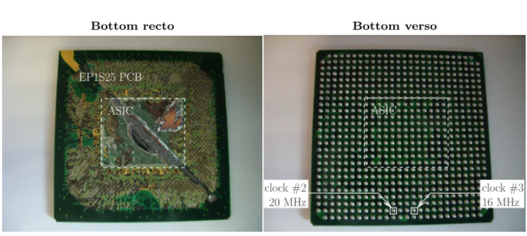
With an eye to comparing the dimensions of this probe with those of a “Logic Array Block” (LAB) of our FPGA, we have depackaged it as visible in Fig. 2. Note nevertheless that none of the analyses reported in the sequel require that the FPGA be depackaged. The ASIC (silicon die) is 1.60 cm wide for 78 LABs and 1.35 cm high for 46 LABs. A Stratix LAB has a width of about 205 µm and a height of about 290 µm; therefore, our probe covers four of them.
The characteristics of the other measurement instruments must be coherent with those of our antenna, notably in terms of bandwidth. There are a set of HZ-16 Rohde and Schwarz pre-amplifiers for an overall gain of 50 dB in the frequency range from 100 kHz to 3 GHz, and an 54855 Infiniium Agilent oscilloscope with a bandwidth of 6 GHz and a maximal sample rate of 40 GSa/s. Tests done by sweeping the antenna over the case of the FPGA show that 50 dB is enough to ensure the use of the full scale of the “Digital to Analog Converter” (DAC) of our oscilloscope.
Bottom recto Bottom verso EP1S25 PCB ASIC clock #3 16 MHz 20 MHz clock #2 ASIC
Fig. 2. The depackaged EP1S25 FPGA, and the two clocks we provide for it.
The antenna, mounted on a 2D motorized table, can cover a maximal area of 2.08 cm × 2.00 cm with a step of 0.1 µm on X and 1 µm on Y. This area is slightly less than that of the case of our FPGA.
The attacked device is a EP1S25 “Stratix” Altera FPGA (130 nanometers tech-nology), embedded on a “SHIX2.0”, an 8-layer PCB professional board (See [Polti 2007]). Note that this FPGA is not EM-shielded, which easies the measurements: in no way do we modify the motherboard, or use chemicals to take off the top of the FPGA case. In that sense, all our analyses are non-invasive [Skorobogatov 2005]. Never-theless, we present in the Section 4.2 attacks which can be use face to EM-shielded FPGA.
Fig. 3 is a photograph of the antenna over the “SHIX2.0” board and the FPGA. We have found that no Faraday cage is needed for the cartographies, because the spatial reactivity of the antennas is accurate enough. A 1:1 scale schematic of the scanned area (with the surrounding decoupling capacitors) is represented in Fig. 4.
3.2 Methodology
To experimentally validate our methods of localization, which will be detailed in the following sub-sections, we built a “radiating” design and then we place it at differents area of the FPGA. If our methods are suitable, we should observe a correlation between the highlighted area in the final EM cartography that they put in evidence and the placement of the design.
The most obvious solution is to build an oscillator, which presents the advantages of standing alone (no inputs have to be generated), of operating and so radiating in the same manner over time, and of being recognizable by its frequency signature. In order that the radiated EM waves have sufficient energy to be detected, not only is the number of elements important, but they should also consume power at the same moment. To use technical terms, they should be synchronized with a master clock.
To reduce the overall noise (the sum of the ambient noise and of the acquisition chain noise) and to enhance the accuracy of the measurements, each acquisition is averaged by the oscilloscope (the resolution of its DAC is also increased by this
op-Fig. 3. The antenna over the “SHIX2.0” board and the FPGA. EP1S25 mini-PCB 3 .4 5 c m ASIC XY-table EP1S25 case 2 .0 0 c m +1.04 cm -1.04 cm
probe clk
rst n enable
256×
Fig. 5. Logic schematic of the oscillator.
eration). Moreover, this guarantees that each acquired measurement trace (further simply referred as “trace”), one per point of the map, has the same shift between its phase and that of the oscillator. This unavoidable care necessitates that the oscilloscope be driven by a trigger signal which is the unique output of our design. To end this list of constraints, there is a last precaution to take in order to make reliable measurements: when building a map, we should be able to detect the radi-ations emitted by our oscillator, and reject those of the trigger signal and its path to the output pin, and those of the master clock and its path from the input pin. One way to solve this problem is to set them up with different and distinguishable frequencies. Consequently, we activate our oscillator during 50 periods of the mas-ter clock, then we disable it for the same number of periods. The resulting signal is “amplitude modulated” (AM), whose carrier frequency is that of the master clock, and whose base-band frequency is 100 times smaller. We activate the trigger signal every 8 periods of our base-band signal.
In conformity with what has been previously written, the final design depicted by Fig. 5 is composed of 512 D-latches contained in a square of 8 × 8 LABs. The number of LE, arbitrary chosen, was proved by further results to be suitable for our experiments. The oscillator is driven by a 20 MHz system clock, modulated by a 200 kHz base-band signal, and activates a synchronizing signal every 40 µs, as visible in the simulation results in Fig. 10. The activity (in terms of number of DFF toggles) is equal to 512 during 50 clock cycles, and then 0 during the next 50 clock cycles.
The purpose of the final AND gate, driving probe, is merely to avoid the synthe-sizer from removing all the logic. During the measurements, of course, the input
enablewas set to ’0’.
We are now going to present you two methods which allow us to locate the chip over its entire case by moving the oscillator from one corner of the chip to each of the other corners, over four successive acquisition campaigns. Fig. 6 shows the placement of our oscillator in the South-West (SW) corner of the FPGA matrix.
3.3 Cartography Methods
To map the FPGA, we take 50 points along both the length and the width of its case. For each of these points, we acquire a trace averaged 16 times, with a window-time duration of 50 µs, which corresponds to 10 periods of the base-band signal. This is long enough to contain two major synchronizing pulses, whose EM radiations can be observed on the Fig. 7. The first one which triggers the oscilloscope is hidden by the X axis, and the second one is at t=40 µs. For the following analysis, we will reduce the time-window to suppress their influence.
8 LABs 1.6 mm 8 LABs 2.3 mm SE SW NW NE
Fig. 6. Placement of our oscillator in the SW corner of the FPGA.
-800 -600 -400 -200 0 200 400 600 0 10 20 30 40 50 V [nV] t [µs] Analysis window
Synchronisation signal influences
0 0.2 0.4 0.6 0.8 1 1.2 1.4 1.6 1.8 V [µV] -1 -0.5 0 0.5 1 X [cm] 0 0.5 1 1.5 2 Y [cm] clock #1 clock #2 oscillator
Fig. 8. Map of maximum EM radiations (NW placement).
3.3.1 Temporal Domain Analysis. Now, to obtain a cartography, we have to
reduce each trace to a single value which will be allocated to one point. To do so, we look over the entire trace for its maximum Peak-to-Peak value, i.e. the maximum amplitude of the EM field envelope. This is a way to highlight areas where EM radiations are maximum.
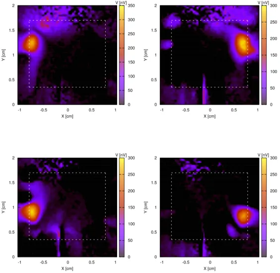
Fig. 8 presents the resulting 50 × 50 point cartography when the oscillator is placed in the NW region. The entire map covers the case of the FPGA, and the dashed rectangle is a landmark which delimits the ASIC of the FPGA (as depicted by the schematic of Fig. 4).
Two areas, marked as clock #1 and #2 (as per Fig. 2), stand out in the middle bottom of the map, whereas we expected to obtain only one in the top left of the map. Hence, the correlation of them with the position of our oscillator is not trivial. More, they are beyond the ASIC zone of demarcation: they correspond to the EM radiation of the solder balls of the mini-PCB supporting the ASIC. As showned in Section 3.3.2, the information they carry are respectively the 20 MHz and the 16 MHz clocks provided for the FPGA.
These clocks blind us: their EM-fields has an amplitude of 1.61 µV (yellow color of the scale), as these of our oscillator, distinguishable in the NW region, is close to 0.40 µV (blue color of the scale), which is four times less.
To filter out these blinding zones, we do an acquisition campaign while the os-cillator is idle. Then, as previously, we compute the new map, and subtract it to the latter. The result for the four placements can be seen in Fig. 9: all common points cancel each others out in the final map, and we are now able to locate our oscillator.
We close this part by having a look at the most radiating point for the NW placement. Their coordinates are X=-0.748 cm and Y=1.240 cm for an amplitude
0 50 100 150 200 250 300 350 V [nV] -1 -0.5 0 0.5 1 X [cm] 0 0.5 1 1.5 2 Y [cm] 0 50 100 150 200 250 300 V [nV] -1 -0.5 0 0.5 1 X [cm] 0 0.5 1 1.5 2 Y [cm] 0 50 100 150 200 250 300 V [nV] -1 -0.5 0 0.5 1 X [cm] 0 0.5 1 1.5 2 Y [cm] 0 50 100 150 200 250 300 V [nV] -1 -0.5 0 0.5 1 X [cm] 0 0.5 1 1.5 2 Y [cm]
Fig. 9. Location of the oscillator in each corner of the FPGA.
of 313.47 nV. The corresponding trace is shown in the Fig. 10. We clearly can see the emitted pattern, which corroborates the previous results.
3.3.2 Frequency Domain Analysis. To perform a frequency domain analysis,
the “Discrete Fourier Transform” (DFT) of each trace is computed. Then, the frequency map is obtained by displaying the amplitude of a chosen frequency com-ponent. This practical method is a refinement of the “Temporal Domain Analysis”: in place of considering the amplitude of the entire signal (i.e. of the sum of its fre-quency components), we can just focus on a particular frefre-quency component. Note,
-1000 -800 -600 -400 -200 0 200 400 600 0 10 20 30 40 50 V [nV] t [µs]
Fig. 10. Trace for X=-0.748 cm and Y=1.240 cm (top) and simulation results (bottom).
that a combination of the frequency components can also be plotted to built the frequency map and improve analysis.
To learn more about the frequency distribution, the average and the variance of the DFT of the previous traces is computed. The average is an image of the present frequencies in the whole of the FPGA, as the variance is an image of the way how the frequencies divide up. For a given frequency, the comparison of its average and its variance informs us about its disparity. For example, a low average can correspond either to a frequency of significant amplitude but very localized in the FPGA, or with a frequency of mean amplitude but present in the whole of the FPGA. The variance allows to raise the doubt; if this one is low, it means that the considered frequency divides up in all the FPGA.
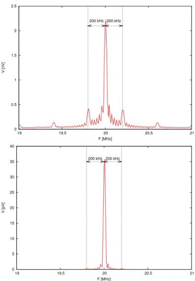
This average and this variance with the oscillator in the NW region are repre-sented on the Fig. 11 for the frequencies between 19 MHz and 21 MHz.
The lobe in the center conveys a component at 20 MHz in the EM collected field. As written in Section 3.3.1, this frequency is the fundamental frequency of one master clock provided for the FPGA. With the above method, we can now prove that the clock #1 and #2 marks of the Fig. 8 correspond respectively to the
0 0.5 1 1.5 2 19 19.5 20 20.5 21 V [nV] F [MHz] 200 kHz 200 kHz 0 5 10 15 20 25 30 35 40 19 19.5 20 20.5 21 V [pV] F [MHz] 200 kHz 200 kHz
Fig. 11. Average (top) and variance (bottom) of the DFT.
20 MHz and 16 MHz clocks.
This proof is given by the Fig. 12 where are drawed up the maps for the ninth harmonic of the 16 MHz clock (160 MHZ) and for the fourth harmonic of the 20 MHz (100 MHz). The oscillator is still place in the NW region.
Returning to Fig. 11, we found 2 secondary lobes, distant from the first one of 200 kHz. These are the frequency signature of our amplitude modulated oscillator. As previously, by focusing in this frequency or its harmonics, we can locate the oscillator over the FPGA. The ideal correlation consists in taking into account the theorical contributions of all the components of the signal.
The result for the four placements can be seen in Fig. 13 when considering the forty-fifth harmonic (920 MHz).
0 2 4 6 8 10 12 14 16 18 20 V [nV] -1 -0.5 0 0.5 1 X [cm] 0 0.5 1 1.5 2 Y [cm] 0 5 10 15 20 25 30 35 40 V [nV] -1 -0.5 0 0.5 1 X [cm] 0 0.5 1 1.5 2 Y [cm]
Fig. 12. 160 MHz (top) and 100 MHz (bottom) maps.
The most radiating frequency component for the NW placement is at X=-0.748 cm and Y=1.240 cm for an amplitude of 0.74 nV. This point is the same as the one found in the section Section 3.3.1. These two methods are coherent since they con-verge to the same solution. But the real test is their efficiency to break a key, which is presented in the next section.
Major conclusion of this study is that EM imaging does not provide an image of the layout, but rather of the leakage. This has been clearly put forward by the comparison of the EM map with the floorplan: the design does not exactly coincide with the observed EM map. For instance, the ring oscillator, placed with a square region, is seen as a circular spot.
0 0.1 0.2 0.3 0.4 0.5 0.6 0.7 0.8 V [nV] -1 -0.5 0 0.5 1 X [cm] 0 0.5 1 1.5 2 Y [cm] 0 0.1 0.2 0.3 0.4 0.5 0.6 0.7 V [nV] -1 -0.5 0 0.5 1 X [cm] 0 0.5 1 1.5 2 Y [cm] 0 0.1 0.2 0.3 0.4 0.5 0.6 0.7 0.8 V [nV] -1 -0.5 0 0.5 1 X [cm] 0 0.5 1 1.5 2 Y [cm] 0 0.1 0.2 0.3 0.4 0.5 0.6 0.7 0.8 V [nV] -1 -0.5 0 0.5 1 X [cm] 0 0.5 1 1.5 2 Y [cm]
Fig. 13. Location of the oscillator in each corner of the FPGA.
the power/ground network, clock trees, pins amplifiers, wire bounding, etc. Unlike other approaches, we do not attempt to provide with an accurate model of theses emanations. Instead, we take on an innovative approach, that consists in consider-ing the raw EM imagconsider-ing as a primary source of information. In the next section, we indeed show that, even without trying to corroborate the EM signals with the layout, we manage to improve the speed of the key extractions.
3.4 Lessons Learnt from Timing and Frequency Domain Analyses
In this section 3, we have shown that raw EM signals are not exploitable as such in the context of an attack. However, we have proposed two techniques to improve the leakage interpretation:
(1) Due to the scalar nature of the EM signals, they can be linearly combined. Therefore, the difference between a map where the module is active and another where it is inactive definitely allows an adversary to locate the co-processor. (2) The spectral separation is also very efficient in telling which module occupies
which portion of the design. This technique does not require to have two car-tographies: one with the co-processor active and another with the co-processor inactive.
An optimal attack uses the two techniques jointly.
4. ATTACK OF A CRYPTOGRAPHIC MODULE
To realize an EM map of a circuit, the analysis can use arbitrary number of mea-surements. It is thus recommended to average the signals, so as to get rid off the noise. It must be noted that when the oscilloscope is in average mode, it does not trigger on every edge of the synchronization signal. Indeed, block encryption is extremely fast (a few clock cycles), and an acquisition apparatus cannot cope with this frequency.
However, in the conditions of a realistic attack, the number of the encryptions must be limited to the strict minimum. We therefore disable the averaging so as to trigger at every edge of the synchronization signal: no single encryption is skipped by the attacker.
4.1 SECMATV3
SECMATV3 [Guilley et al. 2008] is a prototype ASIC, that implements a smart-card (ISO 7816) interface and that is able to realize basic cryptographic operations securely. More specifically, it has been devised to compare the relative strength of
WDDL and Sectionib logics, on the example of the synchronous DES [NIST/ITL/CSD 1999] (or equivalently the “triple-DES”) hardware accelerator [Guilley et al. 2007]. This
prototype ASIC is programmable in the C language, and is fully configurable via an RS232 or a USB port. It supports In situ debug via the step-by-step mode (the circuit has two clocks, one of them being able to load/unload two scan chains of 3400 D flip-flops.) The simulation of the circuit, at RTL and netlist-level (before and after P&R) is fully supported.
SECMATV3 has been ported on an Altera Stratix. The floorplan is given in Fig. 14. Two DES identical unprotected accelerators are studied. They are called DES1 and DES2 in Fig. 14, and sit at the SW and NW corners of the floorplan. They consist in respectively 1155 and 1151 logic elements. A third DES module, implemented in WDDL logic, is located on the east side of the FPGA. Its area is 4121 logic cells.
DES2
DES1
DES in WDDL
Fig. 14. Floorplan of the SECMATV3 system-on-chip programmed in a Stratix.
4.2 EMA as DPA-like
Since the beginning, our idea is to perform the most local possible measurements so that they correspond very faithfully to the energy consumption of the element leaking the most information. We think that this attack is more powerful than a DPA where the measurement is global as it amounts to the consumption of all the attacked circuit.
However, as already presented in [Agrawal et al. 2002], each part of an electronic board radiates EM-field: the attacked circuit, but also its power and data wires. Then, it is possible to get back an image of the global current consumption by harvesting the field emitted by one of the decoupling capacitors of the “Power Distribution Network” (PDN).
We recall that the role of the decoupling capacitors is to bring a response to the need a integrated circuit of high frequencies and transient currents. As a corollary, they are local power sources, that betray the instant current call. They are arranged in network everything around the FPGA, in a way that each feeds a zone of this latter. Therefore they constitute privileged devices for an attacker seeking side-channels. This attack is “DPA-like”, with the advantage to require no modification of the motherboard.
-40 -20 0 20 40 60 80 0 0.5 1 1.5 2 V [nV] t [µs]
Fig. 15. Example of emitted field near a decoupling capacitors.
The EM field that we can collect with an averaging value of 256 is shown on the figure 15. The DES encryption starts at t=0.5 µs.
We lead an attack of this type on the capacitor C43, located on the north face of the FPGA (see Fig. 4). Table I(a) reports the number of “Measurements To Dis-close” (MTD) the key, for the CEMA on the first round of the DES encryption. The results are detailed for each substitution box (sbox) making up the DES datapath. By a way of comparison, we give in Tab. I(b) the MTD for a classic CPA on the same FPGA. These MTD figures have been collected in an acquisition campaign similar to that of [Guilley et al. 2008]. Less than 100,000 encryptions are required to retrieve the correct key (in CPA – in DPA, slightly more traces are needed), which is all the same 3.3 times greater than the DPA-like attack.
This makes clear the point that the leakage map is definitely not centered on the location of the encrypting module. The leak exploited by EMA is not only related to the exact location of the functional gates or wires, because the activity is spread among the global networks (energy supplies and clock buffers). This means that the EM leak is spread in space. Dynamic EM imaging is the adequate tool to localize the most emitting regions. Some of them are localized on decoupling capacitors, but some others can be over the device. We insist that an analytic model [Li et al. 2005] for the leaks map is useless, as the point with greatest leakage can be found by exploring different positions.
Table I. Number of Measurements to Disclose (MTD) the key. (a) CEMA on the C43 capacitor.
Analysis S1 S2 S3 S4 S5 S6 S7 S8
CEMA 4,889 7,548 16,566 16,795 23,648 14,856 30,215 13,684
(b) CPA (current consumed globally by the FPGA).
Analysis S1 S2 S3 S4 S5 S6 S7 S8
CPA 73,702 74,917 43,997 37,833 56,859 55,121 95,294 42,369
(c) CEMA with the Temporal Analysis Method.
Analysis S1 S2 S3 S4 S5 S6 S7 S8
CEMA 1891 7623 1508 3758 2101 1204 1176 226
(d) CEMA with the Frequency Analysis Method.
Analysis S1 S2 S3 S4 S5 S6 S7 S8
CEMA 2887 6296 1096 4732 3056 746 1494 654
(e) CEMA with the antenna on the master clock.
Analysis S1 S2 S3 S4 S5 S6 S7 S8
CEMA failed 44,400 34,354 failed 28,698 failed failed failed
4.3 Cartography
We now get to apply the methods of Section 3.3 to attack the DES1 module of SECMATV3. The temporal window has a duration of 20 µs and includes:
—16 clock cycles during which the DES module is idle; —8 clock cycles during which the key is loaded; —8 clock cycles during which the message is loaded;
—16 clock cycles corresponding to the 16 rounds of the DES encryption.
The temporal differential map of the maximum EM-field Peak-to-Peak value between an active phase and an idle phase of the DES1 module is depicted by Fig. 16.
The most radiating point is at X=-0.707 cm and Y=0.760 cm and has an am-plitude of 103.29 nV. The corresponding trace is shown in the Fig. 17. We can see in its center the influence of the signal of synchronization, and just in its right, we can observe the increase of EM radiation when the encryption starts.
To perform a frequency domain analysis, we should know the frequency signature of the DES1 module. Assuming that the time window contain only one ciphering, these frequency signature can easily be specified: as visible in Fig. 17, the 8.333 MHz master clock of SECMATV3 is amplitude modulated following the activities of the DES1 module. Viewed from the DFT, the period of the modulant signal is equal to the time length of the window analysis. This latter is equal 9.8 µs as marked in Fig. 17. Then, in the DFT, we except a secondaries side-lobes at a distance of 204.064 kHz from harmonics of the master clock. The Fig. 18 is the map for the left secondary lobe of the seventh harmonic (66.471 MHz).
0 20 40 60 80 100 120 V [nV] -1 -0.5 0 0.5 1 X [cm] 0 0.5 1 1.5 2 Y [cm]
Fig. 16. Differential temporal map between a rest and an encryption phases for the DES1 module.
The most radiating frequency component is at X=-0.707 cm and Y=0.800 cm for an amplitude of 0.78 nV. Its distance with the temporal point is only of 40 µm, which is our step resolution on the Y axis. As they are very close, we state once time again the convergence of the two methods. We place now our antenna above the temporal point and launch the attack whose results are presented in the next section.
4.4 Attack Results
As reported in Tab. I(d), we only need 6,296 measurements to disclose all the bits of the key, which is the five as less than for the DPA-like EMA (refer to Tab. I(a) in Section 4.2).
The MTD is slightly higher for the Timing Domain Analysis, as written in Tab. I(c).
These good results are under the condition of a good positioning of the antenna. As an example of a bad positioning, Tab. I(e) gives the results for an attack over the 20 MHz master clock pin.
5. CONCLUSION AND FURTHER WORK
Previous observations as well as novel experiments reported in this article do con-firm that FPGAs leak much information about the internal data they process. For the first time, we successfully realize a cartography of several toy designs imple-mented in deep-submicron technology. We observe that our EM imaging has the
-200 -150 -100 -50 0 50 100 150 0 5 10 15 20 V [nV] t [µs] Encryption
Fig. 17. EM-field above the most leaking point of the DES1 module.
advantage of revealing active regions, which can be useful to locate a particular processor (visible while active – invisible when inactive).
In the context of EM attacks, we insist that the exact localization of the cryp-tographic target is not necessary: the coarse resolution we obtained with our EM imaging is sufficient. We note that the EM imaging does not reveal the exact layout of the FPGA, but instead directly guides the attacker towards the areas that are leaking the most. We achieve successful attacks with an accurate sensor, both far from (namely on a SMC capacitor on the board) and close to (namely directly over the FPGA) the encryption co-processor. As compared to the previously published attacks, we report a successful attack on a DES module in less than 6,300 measure-ments, which is currently the best cracking performance against this encryption algorithm implemented within a complete SoC programmed in an FPGA.
REFERENCES
Agrawal, D., Archambeault, B., Rao, J. R., and Rohatgi, P. 2002. The EM Side-Channel(s). In CHES. LNCS, vol. 2523. Springer, 29–45.
Agrawal, D., Rao, J. R., and Rohatgi, P. 2003. Multi-channel attacks. In CHES. Vol. 2779. Springer, 2–16.
Archambeau, C., Peeters, ´E., Standaert, F.-X., and Quisquater, J.-J. 2006. Template Attacks in Principal Subspaces. In CHES. Vol. 4249. Springer, 1–14.
Brier, ´E., Clavier, C., and Olivier, F. 2004. Correlation Power Analysis with a Leak-age Model. Proc. of CHES’04 3156, 16–29. ISSN: 0302-9743; ISBN: 3-540-22666-4; DOI: 10.1007/b99451; Cambridge, MA, USA.
0 0.1 0.2 0.3 0.4 0.5 0.6 0.7 0.8 V [nV] -1 -0.5 0 0.5 1 X [cm] 0 0.5 1 1.5 2 Y [cm]
Fig. 18. Frequency map at 66.471 MHz for the DES1 module.
Carlier, V., Chabanne, H., Dottax, E., and Pelletier, H. 2005. Generalizing Square Attack using Side-Channels of an AES Implementation on an FPGA. In FPL (2006-01-30), T. Rissa, S. J. E. Wilton, and P. H. W. Leong, Eds. IEEE, 433–437.
Chari, S., Rao, J., and Rohatgi, P. 2002. Template Attacks. In CHES. LNCS, vol. 2523. Springer, 13–28.
Drimer, S. 2008. Volatile FPGA design security – a survey. Version 0.96, http://www.cl.cam.ac.uk/~sd410/papers/fpga_security.pdf.
Dyrkolbotn, G. O. and Snekkenes, E. 2007. A Wireless Covert Channel on Smart Cards (Short Paper). LNCS, vol. 4307. Springer, 249–259. ISSN 0302-9743 (Print) 1611-3349 (Online). Eisenbarth, T., Kasper, T., Moradi, A., Paar, C., Salmasizadeh, M., and Shalmani, M. T. M. 2008. Physical cryptanalysis of keeloq code hopping applications. Cryptology ePrint Archive, Report 2008/058. http://eprint.iacr.org/.
Fahn, P. N. and Pearson, P. K. 1999. IPA: A New Class of Power Attacks. In CHES. LNCS, vol. 1717. Springer Berlin / Heidelberg, 173. Worcester, MA, USA. ISSN 0302-9743.
Gandolfi, K., Mourtel, C., and Olivier, F. 2001. Electromagnetic Analysis: Concrete Re-sults. In CHES. LNCS, vol. 2162. Springer, 251–261.
Guilley, S., Hoogvorst, P., and Pacalet, R. 2004. Differential Power Analysis Model and some Results. In Proceedings of WCC/CARDIS. 127–142. Toulouse, France.
Guilley, S., Hoogvorst, P., and Pacalet, R. 2007. A Fast Pipelined Multi-Mode DES Architecture Operating in IP Representation. Integration, The VLSI Journal 40, 479–489. DOI: 10.1016/j.vlsi.2006.06.004.
Guilley, S., Sauvage, L., Danger, J.-L., Graba, T., and Mathieu, Y. 2008. Eval-uation of Power-Constant Dual-Rail Logic as a Protection of Cryptographic Applications in FPGAs. In SSIRI. IEEE, Yokohama, Japan, 16–23. DOI: 10.1109/SSIRI.2008.31, http://hal.archives-ouvertes.fr/hal-00259153/en/.
solutions to counteract passive and active attacks. In FDTC, 5th workshop on Fault Detection and Tolerance in Cryptography, IEEE-CS. Washington DC, USA, 3–17. (in press – up-to-date version on HAL).
Kocher, P., Jaffe, J., and Jun, B. 1999. Differential Power Analysis. In Proceedings of CRYPTO’99. LNCS, vol. 1666. Springer-Verlag, pp 388–397.
Le, T.-H., Cl´edi`ere, J., Canovas, C., Robisson, B., Servi`ere, C., and Lacoume, J.-L. 2006. A Proposition for Correlation Power Analysis Enhancement. In CHES. LNCS, vol. 4249. Springer, 174–186. Yokohama, Japan.
Li, H., Markettos, A., and Moore, S. 11-14 Oct. 2005. A security evaluation methodology for smart cards against electromagnetic analysis. In Security Technology, 2005. CCST’05. 39th Annual 2005 International Carnahan Conference on. 208–211.
Messerges, T. S., Dabbish, E. A., and Sloan, R. H. 1999. Investigations of Power Analysis Attacks on Smartcards. In USENIX — Smartcard’99. 151–162. Chicago, Illinois, USA. Mulder, E. D., Buysschaert, P., ¨Ors, S. B., Delmotte, P., Preneel, B., Vandenbosch, G., and Verbauwhede, I. 2005. Electromagnetic Analysis Attack on an FPGA Implementation of an Elliptic Curve Cryptosystem. In IEEE International Conference on Computer as a tool (EUROCON). Belgrade, Serbia & Montenegro. http://www.eurocon2005.org.yu/.
NIST/ITL/CSD. 1999. Data Encryption Standard. FIPS PUB 46-3. http://csrc.nist.gov/publications/fips/fips46-3/fips46-3.pdf.
¨
Ors, S. B., Oswald, E., and Preneel, B. 2003. Power-Analysis Attacks on an FPGA: First Experimental Results. In CHES. Vol. 2779. Lecture Notes in Computer Science, Springer-Verlag, 35–50.
Peeters, ´E., Standaert, F.-X., Donckers, N., and Quisquater, J.-J. 2005. Improved Higher Order Side-Channel Attacks with FPGA experiments. In Cryptographic Hardware and Em-bedded Systems - Proceedings of CHES 2005, J. R. Rao and B. Sunar, Eds. LNCS, vol. 3659. Springer-Verlag, 309–323.
Peeters, ´E., Standaert, F.-X., and Quisquater, J.-J. 2007. Power and electromagnetic anal-ysis: Improved model, consequences and comparisons. Integration, The VLSI Journal, special issue on “ Embedded Cryptographic Hardware” 40, 52–60. DOI: 10.1016/j.vlsi.2005.12.013. Polti, A. 2007. STRATIX – SH4 prototype PCB for high-performance embedded systems. http://www.enst.fr/~polti/realisations/shix20/.
Quisquater, J.-J. and Samyde, D. 2001. ElectroMagnetic Analysis (EMA): Measures and Counter-Measures for Smard Cards. In Smart Card Programming and Security (E-smart 2001), I. Attali and T. P. Jensen, Eds. LNCS, vol. 1240. Springer-Verlag, 200–210. ISSN 0302-9743. Rechberger, C. and Oswald, E. 2004. Practical Template Attacks. In WISA. LNCS, vol. 3325. Springer, 443–457.
Rohde and Schwarz. R&S HZ-15 Probe Set. Website: http://www2.rohde-schwarz.com/product/HZ15.html.
Skorobogatov, S. P. 2005. Semi-Invasive Attacks — A new approach to hardware security analysis. Ph.D. thesis, Cambridge University / Computer Laboratory, Secu-rity Group, TAMPER laboratory. Technical Report UCAM-CL-TR-630, ISSN 1476-2986, http://www.cl.cam.ac.uk/techreports/UCAM-CL-TR-630.pdf.
Skorobogatov, S. P. 2006. Optically Enhanced Position-Locked Power Analysis. In CHES. LNCS, vol. 4249. Springer, 61–75.
Standaert, F.-X., ¨Ors, S. B., and Preneel, B. 2004. Power Analysis of an FPGA: Im-plementation of Rijndael: Is Pipelining a DPA Countermeasure? In CHES. LNCS, vol. 3156. Springer-Verlag, 30–44.
Standaert, F.-X., Peeters, ´E., Mac´e, F., and Quisquater, J.-J. 2006. Updates on the Security of FPGAs Against Power Analysis Attacks. In ARC. LNCS, vol. 3985. Springer-Verlag, 335–346. Delft, The Netherlands.
Standaert, F.-X., Peeters, ´E., Rouvroy, G., and Quisquater, J.-J. 2006. An Overview of Power Analysis Attacks Against Field Programmable Gate Arrays. Proceedings of the IEEE 94, 2 (February), 383–394. Invited Paper.