HAL Id: hal-01307936
https://hal.archives-ouvertes.fr/hal-01307936
Submitted on 27 Apr 2016
HAL is a multi-disciplinary open access
archive for the deposit and dissemination of sci-entific research documents, whether they are pub-lished or not. The documents may come from teaching and research institutions in France or abroad, or from public or private research centers.
L’archive ouverte pluridisciplinaire HAL, est destinée au dépôt et à la diffusion de documents scientifiques de niveau recherche, publiés ou non, émanant des établissements d’enseignement et de recherche français ou étrangers, des laboratoires publics ou privés.
Equivalent circuit of a reconfigurable triple-slot
reflectarray cell
Kevin Nadaud, Raphaël Gillard, Erwan Fourn, Hartmut W. Gundel
To cite this version:
Kevin Nadaud, Raphaël Gillard, Erwan Fourn, Hartmut W. Gundel. Equivalent circuit of a recon-figurable triple-slot reflectarray cell. IET Microwaves Antennas and Propagation, Institution of Engi-neering and Technology, 2016, 10 (10), pp.1080-1086. �10.1049/iet-map.2015.0378�. �hal-01307936�
This paper is a postprint of a paper submitted to and accepted for publication in IET Microwaves, Antennas & Propagation and is subject to Institution of Engineering and Technology Copyright.
The copy of record is available at IET Digital Library
Equivalent circuit of a reconfigurable triple-slot reflectarray cell
Kevin Nadaud1, Raphaël Gillard2,*, Erwan Fourn2, Hartmut W. Gundel1
1IETR UMR CNRS 6164, University of Nantes, 2 rue de la Houssinière, Nantes, France
2IETR UMR CNRS 6164, INSA of Rennes, 20 avenue des Buttes de Coësmes CS 70839, Rennes,
France
Abstract: Abstract : This paper presents an equivalent model for a multiple-resonance reflectar-ray cell. It allows predicting the different phase-states of the cell from only a very few full-wave simulations. Demonstrations are first given for a passive cell where different geometrical param-eters are varied. Then, the approach is generalized to a reconfigurable cell. Finally, a canonical reflectarray with a steered beam has been synthesized in order to illustrate the capabilities of the proposed equivalent circuit.
1. Introduction
Reflectarrays are widely studied because they combine the advantages of reflector antennas and array antennas. In order to increase bandwidth and reduce losses, multiple-resonator cells have been proposed, using various topologies such as stacked patches [1], coupled dipoles [2] or cou-pled slots [3]. All these passive cells involve many geometrical parameters, which makes their optimization process complex and time-consuming as it relies on full-wave simulations.
In the case of reconfigurable cells, the situation is even trickier as successive steps have to be completed. First, the passive distributed structure of the cell has to be designed (as in the case of passive cells). Then, lumped reconfigurable elements have to be implemented to control the reflected phase within a prescribed range. Finally, a redesign of the initial passive distributed structure is usually necessary to take into account the biasing lines and other topological arrange-ments resulting from the integration of these tuning elearrange-ments. Although the compression approach
can advantageously be used [4] for tuning lumped elements, the design and redesign of the passive distributed structure still require numerous full-wave simulations.
On the other hand, efficient synthesis processes have been developed in the field of frequency selective surfaces (FSS) [5,6] which replace the full-wave simulations by circuit-based approaches. First, an equivalent circuit for the passive distributed structure is derived using a limited number of full-wave simulations. This provides a direct correspondence between the geometrical parameters and the related circuit elements. Then, any further modification of these geometrical parameters can be analyzed at the circuit level without any additional full-wave simulation. This definitively makes the optimization process simpler and much faster. In [7, 8], an equivalent circuit has been proposed for a slot-loaded patch reflectarray cell. It permits to optimize the number and the place-ment of the lumped components used for changing the reflected phase. Nevertheless, this equiva-lent circuit does not permit to obtain the lengths of the slots or of the patch. In [9] a model is given for a patch loaded with varicap diodes but it has only one resonator, leading to a high frequency dispersion.
In this paper, we present an equivalent circuit for the reflectarray triple-slot cell described in [3]. Although this cell has been proved to be a good candidate for both, large bandwidth and reconfig-urability, no simple process has been reported yet to optimize its dimensions. The proposed circuit allows predicting the phase response when the slots length (the most influent parameters) and the distance to the ground plane change. Only a limited number of simulations is needed, which is essential for fast optimization. In a first time, the interest of this approach is validated for the design of a passive cell. Then, we show that it can be extended to the analysis of a reconfigurable cell by combining the equivalent circuit of the passive distributed structure with lumped elements that represent the controllable tuning components. Experimental validations at the cell level have already been published [3, 10, 11] for quite similar structures and will not be repeated here for the sake of brevity. We rather focus on the comparison of the results provided by our new equivalent circuit with those resulting from full-wave simulations, with the clear goal to replace those ones.
Finally, the utility of the equivalent circuit is demonstrated by simulating a reflectarray with a steered beam.
Note that the proposed equivalent circuit has similarities with that used in [12, 13] for slotted waveguides. However, our formulation takes mutual coupling between slots into account. Ad-ditional elements are also included to provide a realistic modelling when active components are
integrated in the slot.
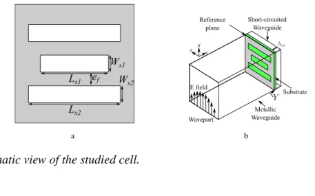
2. Studied topology and associated equivalent circuit
The general studied topology (Fig. 1) consists of three slots in a metallization printed on a dielectric substrate (permittivity 2.17, loss tangent 9 × 10⁻⁴ and thickness 1.6 mm). This printed circuit is suspended in a square waveguide at a distance hair from the short-circuited termination (Fig. 2).
This waveguide configuration is usually used for single cell measurement (as in [11] for instance). Moreover, reflectarray cells (especially active ones) are sometimes embedded in metallic cavities to limit mutual coupling. In such situations, the waveguide between the printed circuit and the short-circuit plane is really present [14]. The section of the square waveguide used here is 35 × 35 mm2
providing a [4.5, 6.5] GHz frequency band.
The reflected phase can be controlled by changing only the length of the central slot or loading it by a tunable capacitor [3]. The other parameters, especially the length of the external slots Ls2,
allow controlling the frequency dispersion and the accessible phase range. Note that both external slots have the same length in order to maintain the cell symmetry. Ls1and Ls2are definitively the
most influent parameters regarding the phase response of the cell and are the only ones to be varied in this study. This choice is also consistent with the fact that, in a realistic reflectarray synthesis, the number of tunable parameters has to be small to keep the optimization process affordable. The variation ranges for Ls1 and Ls2 have been chosen in order to approach a full 360° phase range
at center frequency, which is the usual goal when designing a reflectarray cell. In the considered examples, Ws1 and Ws2 are set to a quite large value (5 mm) in order to achieve smooth phase
states [15]. The distance between adjacent slots ef is set to 2 mm to keep enough space for a future
biasing circuit. Nevertheless, the discussed methodology is also valid in the case of any other values.
The proposed equivalent circuit consists of a shunt admittance (for the printed circuit) backed by a short-circuited transmission line of length hair. The admittance is composed of three shunt
resonators, one for each slot (Fig. 3), which are coupled with inductive (Mc) and capacitive (Cc)
elements. Both types of coupling are necessary to correctly take into account all interactions between the different slots [16]. The propagation characteristics of the transmission line backing the printed circuit are calculated using simple rectangular waveguide theory [17]. The lumped
Ls1 Ls2 Ws1 Ws2 ef a Reference plane Metallic Waveguide Waveport E field Short-circuited Waveguide y x z hair Substrate b
Figure 1. Schematic view of the studied cell. a top view
b 3D view
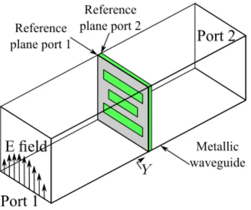
elements forming the shunt admittance itself can be derived from a full-wave simulation using Ansys HFSS commercial software. To do so, the printed circuit is simulated as a 2-port in the waveguide (Fig. 2). One reference plane is placed on each face of the dielectric substrate. The simulated 2 × 2 scattering matrix is then imported into a circuit simulator (Keysight ADS) and the elements of the shunt admittance are tuned until its scattering parameters match those from the full-wave simulation.
Then, the reflected coefficient from the whole cell (including the short-circuited waveguide) can be obtained directly with the circuit simulator simply by loading the obtained admittance with the appropriate length of short-circuited transmission line. As hair can be varied in the circuit
simula-tion itself, the modificasimula-tion of this parameter does not require any addisimula-tional full-wave simulasimula-tion, which is a first advantage of the equivalent circuit. The second advantage, as described in the next section, is the possibility to express the elements forming the admittance from the variable geomet-rical parameters (here Ls1and Ls2). Once these expressions have been derived, which requires only
2 or 3 full-wave simulations, the response of the cell for any value of Ls1 and Ls2 can be obtained
directly from the circuit simulator, without any new full-wave analysis.
3. Derivation of the equivalent circuit
3.1. General Process
In this section, the derivation of the elements of the equivalent circuit from full-wave simulations is described in details. As a first approximation, we consider that C1 and L1 only depend on Ls1
Reference plane port 1 Metallic waveguide Port 1 E eld Reference plane port 2 Port 2
Figure 2. Schematic view of the waveguide containing the cell simulated with HFSS.
Port 1 Cell Port 2 Waveguide
Figure 3. Proposed equivalent circuit of the triple-slot cell.
while C2and L2only depend on Ls2. Ccand Mcare supposed to be independent from both Ls1and
Ls2. As will be seen from the obtained results, this assumption proves to be sufficient. Moreover,
Li and Ci are linked by the following relations:
fi = 1 2π√CiLi and Zi = π 2 r Li Ci , (1)
where fi and Zi stand for the resonant frequency and the characteristic impedance of slot i. Since
the resonant frequency of a transmission line resonator varies with the inverse of its length, we can express fias:
fi =
1 αiLsi+ βi
, (2)
where αi and βi are unknown parameters to be determined. Note that αi is supposed to be close
to 2√εreff/c for a half wavelength slot (with c the speed of light and εreff the effective relative
it represents possible reactive effects which may be responsible for resonance deviations. Finally, using (1) and (2), Ci and Li can be related directly to the length of the slot as:
Ci = αiLsi+ βi 4Zi and Li = Zi(αiLsi+ βi) π2 . (3)
The derivation of the electric circuit then consists in determining Cc, Mc, α1, β1, Z1, α2β2 and
Z2 from a reduced number of full-wave simulations. Once this has been done, Ci and Li can be
calculated for any new value of Lsi using (3). This allows using the electric circuit (instead of a
new EM simulation) for characterizing the phase response of the cell whatever the value of the slots length.
3.2. Validation with variable internal slot and fixed external slots
For the sake of simplicity, we first present the derivation process where only the length of the central slot Ls1varies (L2and C2are supposed to be constant in this case). Two full-wave
simula-tions are run. They correspond to two printed circuits in the waveguide (Fig. 2), only differing in the length of the central slot (L0
s1 and L 00
s1 for the first and second simulation respectively). Then,
two equivalent shunt admittances are tuned simultaneously so that the corresponding S parameters match those of the two simulated structures in the [4.5, 6.5] GHz frequency band. Only C1 and
L1 differ from one admittance to another: we name C01and L01 (respectively C100and L001) the values
associated to L0s1 (respectively L00s1). The tuning process also provides Cc, Mc, C2 and L2 but it
assumes they are identical for both admittances. Finally, α1and β1 can be derived from (3) using:
α1 = 2π pC0 1L 0 1− pC 00 1L 00 1 L0 s1− L 00 s1 , (4) β1 = 2π q C01L01− L0s1α1, (5)
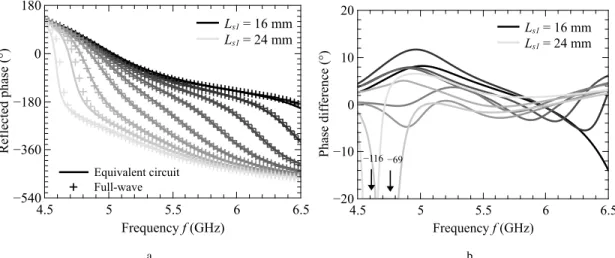
Once the elements forming the shunt admittance have been identified, the full equivalent circuit of the reflectarray cell can be constructed by adding the short-circuited transmission line. The reflected phase obtained from full-wave simulations and the results from the equivalent circuit simulations are compared in Fig. 4a. The extraction of the parameters has been carried out using L0
s1 = 18 mm and L 00
R ef le ct ed p ha se ( °) −540 −360 −180 0 180 Frequency f (GHz) 4.5 5 5.5 6 6.5 Ls1 = 16 mm Ls1 = 24 mm Equivalent circuit Full-wave a P ha se d if fe re nc e (° ) −20 −10 0 10 20 Frequency f (GHz) 4.5 5 5.5 6 6.5 −116 −69 Ls1 = 16 mm Ls1 = 24 mm b
Figure 4. Reflected phase and phase difference as a function of frequency obtained from full wave HFSS simulation (+) and predicted with the proposed equivalent circuit (—). Ls2 = 27 mm, Ls1
varies from16 to 24 mm in steps of 1 mm. a Reflected phase.
b Phase difference.
L2 = 5.69 nH, Cc = 44.8 fF, Mc = 0.68 nH, α1 = 7.59 × 10⁻⁹Hz−1m−1, β1 = 3.09 × 10⁻¹¹Hz−1
and Z1 = 99.7 Ω.
As can been seen in Fig. 4a, the agreement is very good even though Ls1 varies from 16 to
24 mm, which is a larger range than the initial [L0s1, L00s1] interval. Fig. 4b shows the difference between the full wave simulation and the equivalent circuit. For Ls1less than 22 mm, the maximum
phase difference is 12°. For the larger lengths (Ls1 = 23 mm or 24 mm), the phase difference is
much higher at low frequencies. This is due to rapid variation of the phase in that region. Indeed, this corresponds to a high frequency dispersion region (involving resonance phenomena) where the cell is not supposed to be used. For the central frequency (5.5 GHz) the maximum error is 5°. Finally, the average phase difference for all lengths Ls1 over the total frequency band is 4.11°,
which provides a sufficient accuracy for reflectarray design.
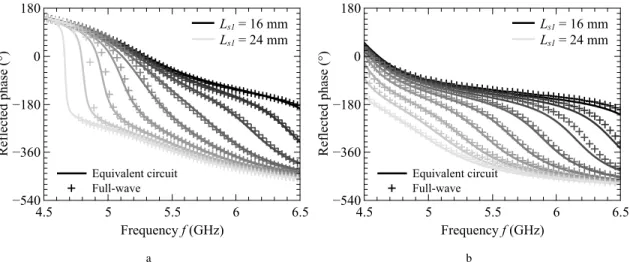
3.3. Validation with variable internal and external slots
Now we consider Ls2 can also vary, which means that α2 and β2 have to be determined. The
derivation process described in section 3.2 can be extended straight forwardly. The new process relies on three full-wave simulations involving the following length couples (L0s1, L0s2), (L00s1, L0s2) and (L0
s1, L 00
s2). Then, three admittances (instead of two) are tuned simultaneously. The first two
R ef le ct ed p ha se ( °) −540 −360 −180 0 180 Frequency f (GHz) 4.5 5 5.5 6 6.5 Ls1 = 16 mm Ls1 = 24 mm Equivalent circuit Full-wave a R ef le ct ed p ha se ( °) −540 −360 −180 0 180 Frequency f (GHz) 4.5 5 5.5 6 6.5 Equivalent circuit Full-wave Ls1 = 16 mm Ls1 = 24 mm b
Figure 5. Reflected phase simulated with HFSS (+) and predicted with the equivalent circuit (—) for variable Ls1 with a step of1 mm.
a Ls2 = 25 mm
b Ls2 = 31 mm
Table 1. Extracted coefficients for passive and active cases.
α1(Hz−1m−1) β1(Hz−1) Z1(Ω) α2(Hz−1m−1) β2(Hz−1) Z2(Ω) Mc(nH) Cc(fF) Lp(nH) Cp(fF)
Passive 7.59 × 10⁻⁹ 3.09 × 10⁻¹¹ 99.7 7.74 × 10⁻⁹ 1.79 × 10⁻¹¹ 243 0.680 44.8 — —
Active 1.27 × 10⁻⁸ −8.38 × 10⁻¹¹ 188 7.33 × 10⁻⁹ 2.79 × 10⁻¹¹ 232 0.343 19.8 4.19 73.8
indicated, the associated admittances only differ in C1and L1. We note C20 and L 0
2the values of C2
and L2for these configurations. The third full-wave simulation (L0s1, L00s2) leads to a different value
of C2and L2, referred to as C002 and L002. Finally, the whole tuning process allows determining α2and
β2 using (4) and (5). Of course, it also provides all the other parameters (as in section 3.2). Note
that Mc and Cc are kept identical for all three admittances since we assume that mutual coupling
does not change significantly when the slots length are varied. This assumption is reasonable as the required variation for Lsi (in order to achieve a full 360° range) is small. Also, since we
use multiple slots, only smooth resonances (and subsequently smooth variations in coupling) are encountered. In this extraction process, the used values of L0s1 and L00s1 are the same as previously and those for L0
s2and L 00
s2are 27 and 29 mm respectively.
Two examples, comparing the results from full-wave and equivalent circuit simulations, are shown in Fig. 5. Both length Ls1 and Ls2 are modified simultaneously. As can be seen from the
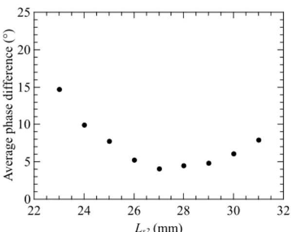
figure, the prediction of there is a quite good agreement. To better evaluate the validity of the model, the average phase difference between the full-wave and the circuit simulations is reported in Fig. 6 as a function of the slot length Ls2. This difference, which is the average difference
A ve ra ge p ha se d if fe re nc e (° ) 0 5 10 15 20 25 Ls2 (mm) 22 24 26 28 30 32
Figure 6. Average phase difference between equivalent circuit and full-wave simulations as a function of the length of the external slot Ls2.
for all lengths Ls1 over the total frequency band, is below 10° for a variation of the external slot
of ±3.5 mm. This difference is attributed to two main causes. Firstly, error logically gets larger when the considered Lsiis outside the [L0si,L00si] extraction range, because extrapolation is required.
Secondly, it is also partly due to the fact we assume that coupling is independent from Lsi.
4. Extension to the active case
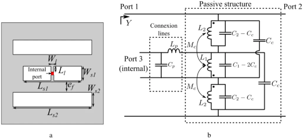
The circuit presented in the first part of this communication is now upgraded for the study of a reconfigurable cell. In the considered example, reconfiguration is achieved by loading the internal slot with a controllable capacitance C (as in [11]). A typical implementation is shown in Fig. 7a. Note that two narrow metallic strips are used for the connection of the lumped element (variable capacitance) in the slot center.
The equivalent admittance is modified as shown in Fig. 7b: a capacitance Cpand an inductance
Lphave been added to represent the capacitive effect of the gap supporting the lumped element and
the inductive effect of the metallic strips respectively.
The extraction of the circuit elements using full-wave simulations is very similar to these de-scribed in the previous sections. In the full-wave simulation, a lumped port (Fig. 7a), corresponding to the third port in the model (Fig. 7b), is added for the extraction of the equivalent circuit. This third port is similar to those used in the compression approach [4] and will provide the place to connect the variable capacitor during the post-processing, after the equivalent circuit extraction. Before that, as in 3.3, three full-wave simulations, involving three different combinations of Ls1
Ws1 Internal port Ws2 Wl Ll Ls1 Ls2 ef a Passive structure Connexion lines Port 3 (internal) Port 1 Port 2 b
Figure 7. Schematic view of the studied cell with an internal port (a) and the proposed equivalent circuit (b).
and Ls2, are necessary to anticipate any future variation of slots length. More precisely and as
previously, the circuit elements shown in Fig. 7b are adjusted so that the resulting S parameters best match those from the full-wave simulations. Note that there are now 3 ports in the equivalent circuit and thus 9 scattering parameters (instead of 4) have to be matched during the extraction process. The values of Lp and Cpare determined during the tuning process, together with all other
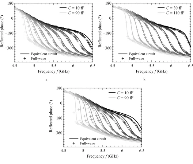
circuit elements, and they are supposed to be identical for the three equivalent admittances. Once the equivalent circuit is derived, it can be loaded with any lumped element simply by connecting it to port 3 as a post-processing step. As previously, this can be combined with any modification of the slots length. The reflected phase for both full-wave simulations and circuit sim-ulations for different slot configurations and various values of the loading element (here a simple capacitance) are compared in Fig. 8. The capacitance range has been adjusted for each couple of lengths in order to keep the resonances in the [4.5, 6.5] GHz frequency band. The three simulations used for the extraction the different parameters are: (L0s1 = 12 mm, L0s2 = 27 mm), (L00s1 = 16 mm, L0s2= 27 mm) and (L0s1 = 12 mm, L00s2 = 29 mm). The average phase difference over the three cases is 8.6° and is respectively indicated in the figure caption. The equivalent circuit permits to predict the reflected phase with a reasonably good precision when one or both slots length are modified. The extracted values are given in Tab. 1.
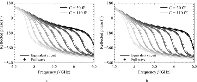
Fig. 9 shows that the proposed equivalent circuit still provides satisfactory results when the air gap between the substrate and the short circuit is modified. The accuracy is better than 7° in all cases.
R ef le ct ed p ha se ( °) −360 −180 0 180 Frequency f (GHz) 4.5 5 5.5 6 6.5 C = 10 fF C = 90 fF Equivalent circuit Full-wave a R ef le ct ed p ha se ( °) −360 −180 0 180 Frequency f (GHz) 4.5 5 5.5 6 6.5 C = 30 fF C = 110 fF Equivalent circuit Full-wave b R ef le ct ed p ha se ( °) −360 −180 0 180 Frequency f (GHz) 4.5 5 5.5 6 6.5 C = 10 fF C = 90 fF Equivalent circuit Full-wave c
Figure 8. Simulated reflected phase with HFSS (+) and predicted with the proposed equivalent circuit (—) for different values of the capacitance C in steps of 10 fF and different couples (Ls1,
Ls2).
a (Ls1, Ls2)= (14 mm, 27 mm), average phase difference: 7.6°
b (Ls1, Ls2)= (12 mm, 25 mm), average phase difference: 6.8°
R ef le ct ed p ha se ( °) −540 −360 −180 0 180 Frequency f (GHz) 4.5 5 5.5 6 6.5 C = 30 fF C = 110 fF Equivalent circuit Full-wave a R ef le ct ed p ha se ( °) −540 −360 −180 0 180 Frequency f (GHz) 4.5 5 5.5 6 6.5 C = 30 fF C = 110 fF Equivalent circuit Full-wave b
Figure 9. Reflected phase simulated with HFSS (+) and predicted with the equivalent circuit (—) for different values of the capacitance C in steps of 10 fF and for two different air gaps between the cell and the end of the waveguide with Ls1 = 12 mm and Ls2= 27 mm.
a hair = 13.7 mm
b hair = 17.7 mm
5. Application of the equivalent circuit
To demonstrate the capabilities of the proposed equivalent circuit, it has been used to synthesize a canonical reflectarray with a steered beam. In order to make a comparison with full-wave simula-tion feasible, it consists of an 8 × 6 array with λ0/1.56 inter-element spacing (35 mm at 5.5 GHz)
as shown in Fig. 10. For the sake of numerical validation, it is illuminated by a plane wave under normal incidence. The length of the central slot varies with the y coordinate so that the beam is steered at θ = 10° in the (yOz) plane. The necessary phase difference between adjacent cells is 40° and the equivalent circuit is used for determining the corresponding length of the central slots. For the presented example, the length of the external slot Ls2has been fixed to 29 mm and is kept
constant for all the cells.
Using the equivalent circuit, the total time to synthesize the array (including the construction of the equivalent circuit itself) is less than 5 minutes on a standard PC workstation (16 GB RAM, Intel® Core™ i7-4790 @ 3.6 GHz). Using full-wave simulations instead would dramatically in-crease the computation burden (especially in the case of an even larger array). The values of the elements in the equivalent circuit are those given in Table 1. The needed lengths to satisfy the phase-law are given in Table 2. To verify the synthesis approach using the equivalent circuit, a full-wave simulation of the complete array has been done using HFSS (which takes 2 hours).
y
x
1
2
3
4
5
6
7
8
identica
l
Figure 10. Schematic view of the proposed reflectarray. The central slot lengths vary from column 1 to 8 but are identical into each column.
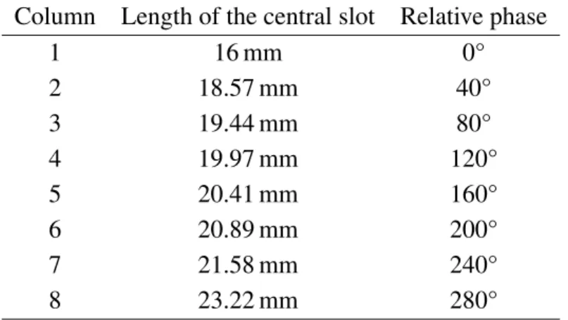
Table 2 Length of the central slot for each column and reflected phase difference with the first column.
Column Length of the central slot Relative phase
1 16 mm 0° 2 18.57 mm 40° 3 19.44 mm 80° 4 19.97 mm 120° 5 20.41 mm 160° 6 20.89 mm 200° 7 21.58 mm 240° 8 23.22 mm 280°
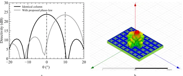
Fig. 11 presents the directivity of the reference array (with all central slots measuring 20 mm long) and the array with the lengths obtained previously. This clearly demonstrates that the beam has been steered properly.
6. Conclusion
In this paper, an equivalent circuit is proposed for a triple-slot phase-shifting cell. This model describes precisely the behavior of the cell and allows predicting the reflected phase while needing only a limited number of full-wave simulations. Both the lengths of the slots and the distance between the cell and the end of the waveguide can be modified. An upgraded version of the equivalent circuit has also been proposed which enables the integration of lumped elements for an active control of the cell. Finally, the equivalent model permits to optimize the slots length of
D ir ec ti vi ty ( dB ) 0 5 10 15 20 25 30 θ (°) −20 −10 0 10 20 Identical column With proposed phase-law
a b
Figure 11. Directivity and 3D radiation pattern of the reflectarray with identical column and with the calculated phase-law.
a Directivity in the (yOz) plane (H-plane). b 3D radiation pattern.
the distributed passive structure with a limited number of full-wave simulation. The comparison with full-wave simulations clearly demonstrates the capability of the equivalent circuit approach to synthesize a reflectarray with a steered beam.
Acknowledgements
The authors would like to acknowledge the CNRS (Centre National de la Recherche Scientifique) and the French Region “Pays de la Loire” for the financial support.
7. References
[1] Encinar, J., Arrebola, M., Dejus, M., et al.: ‘Design of a 1-metre reflectarray for dbs appli-cation with 15 % bandwidth,’ ‘6th European Conf. Antennas Propag. (EUCAP),’ 2006 pp.
1–5
[2] Perez-Palomino, G., Baine, P., Dickie, R., et al.: ‘Design and experimental validation of liq-uid crystal-based reconfigurable reflectarray elements with improved bandwidth in F-band,’ IEEE Trans. Antennas Propag., 2013, 61 (4), pp. 1704–1713
[3] Makdissy, T., Gillard, R., Fourn, E., et al.: ‘Triple-slot phase-shifting cell loaded with capac-itances for reflectarray applications,’ ‘6thEuropean Conf. Antennas Propag. (EUCAP),’ 2012
pp. 3703–3706
[4] Kunisch, J., Rittweger, M., Heinen, S., et al.: ‘The compression approach: A new tech-nique for the analysis of distributed circuits containing nonlinear elements,’ ‘21st European Microwave Conference,’ volume 2, 1991 pp. 1296–1301
[5] Al-Joumayly, M., Behdad, N.: ‘A new technique for design of low-profile, second-order, bandpass frequency selective surfaces,’ IEEE Trans. Antennas Propag., 2009, 57 (2), pp. 452–459
[6] Behdad, N., Al-Joumayly, M. a.: ‘A generalized synthesis procedure for low-profile, frequency selective surfaces with odd-order bandpass responses,’ IEEE Trans. Antennas Propag., 2010, 58 (7), pp. 2460–2464
[7] Tahir, F., Aubert, H., Girard, E.: ‘Optimisation of mems-controlled reflectarray phase shifter cell,’ Microwaves, Antennas Propagation, IET, Feb 2011, 5 (3), pp. 271–276
[8] Tahir, F. A., Aubert, H., Girard, E.: ‘Equivalent electrical circuit for designing mems-controlled reflectarray phase shifters,’ Progress In Electromagnetics Research, 2010, 100, pp. 1–12
[9] Hum, S., Okoniewski, M., Davies, R.: ‘Modeling and design of electronically tunable reflec-tarrays,’ IEEE Trans. Antennas Propag., 2007, 55 (8), pp. 2200–2210
[10] Nadaud, K., Gillard, R., Fourn, E., et al.: ‘A simple Phase-Shifting cell for reflectarray using a slot loaded with a ferroelectric capacitor,’ ‘Loughborough Antennas Propag. Conf.’, 2014 pp. 214–217
[11] Nadaud, K., Gillard, R., Fourn, E., et al.: ‘A triple-slot active reflectarray cell using a ferro-electric capacitor,’ ‘9th European Conf. Antennas Propag. (EuCAP),’ 2015
[12] Eshrah, I. A., Kishk, A. A., Yakovlev, A. B., et al.: ‘Analysis of waveguide slot-based struc-tures using wide-band equivalent-circuit model,’ IEEE Trans. Microw. Theory Tech., 2004, 52 (12), pp. 2691–2696
[13] Eshrah, I. A., Kishk, A. A., Yakovlev, A. B., et al.: ‘Load-independent equivalent circuit model for transverse waveguide slots,’ Progress In Electromagnetics Research, 2007, 69, pp. 1–20
[14] Cheymol, C., Dousset, T., Dumon, P., et al.: ‘A X-band electronically scanned reflectarray antenna for space telemetry,’ ‘3th European Conf. Antennas Propag. (EUCAP),’ March 2009 pp. 2766–2768
[15] Moustafa, L., Gillard, R., Peris, F., et al.: ‘The phoenix cell: A new reflectarray cell with large bandwidth and rebirth capabilities,’ IEEE Antennas Wireless Propag. Lett., 2011, 10, pp. 71–74
[16] Hong, J.-S.: Microstrip Filters for RF/Microwave Applications (John Wiley & Sons, Inc.), chapter Coupled-Resonator Circuits, pp. 193–231, 2011