HAL Id: hal-02298416
https://hal.archives-ouvertes.fr/hal-02298416
Preprint submitted on 12 Feb 2020
HAL is a multi-disciplinary open access
archive for the deposit and dissemination of
sci-entific research documents, whether they are
pub-lished or not. The documents may come from
teaching and research institutions in France or
abroad, or from public or private research centers.
L’archive ouverte pluridisciplinaire HAL, est
destinée au dépôt et à la diffusion de documents
scientifiques de niveau recherche, publiés ou non,
émanant des établissements d’enseignement et de
recherche français ou étrangers, des laboratoires
publics ou privés.
Design and Optimization of a Wideband Metamaterial
Absorber Made of Composite Materials
Olivier Rance, Anne-Claire Lepage, Xavier Begaud, Michel Soiron, André
Barka, Patrick Parneix
To cite this version:
Olivier Rance, Anne-Claire Lepage, Xavier Begaud, Michel Soiron, André Barka, et al.. Design and
Optimization of a Wideband Metamaterial Absorber Made of Composite Materials. 2020.
�hal-02298416�
APPLIED PHYSICS A – EXTENSION FROM META 2018 CONFERENCE PAPER “WIDEBAND METAMATERIAL ABSORBER MADE OF COMPOSITE MATERIALS”
Design and Optimization of a Wideband Metamaterial Absorber
Made of Composite Materials
Olivier Rance
1, Anne Claire Lepage
1, Xavier Begaud
1,
Michel Soiron
2, André Barka
3, and Patrick Parneix
41LTCI, Télécom ParisTech, Université Paris-Saclay, France 2SART, France
3ONERA/DEMR, Université de Toulouse, France 4Naval Group, France
*corresponding author, E-mail: [email protected]
Abstract
Using structural composite materials for the fabrication of Radar Absorbing Materials (RAM) allows combining the strong load bearing capability with the radar absorbing functionality in a unique structure. This article shows the possibility to transpose an already existing metamaterial absorber to the domain of composite materials. The dielectric layers of the absorber initially designed with radio-frequency (RF) materials are replaced with fiber-reinforced composite materials and their thickness is optimized again. The working principle of the absorber is explained layer by layer on the Smith chart. The performances of the composite absorber are compared against the initial RF design and against other classical absorbers. The composite design has a total thickness of 8.9 mm and achieves a reflection coefficient below -14 dB within the band 4.6 GHz - 17.2 GHz at normal incidence. The reflection coefficient remains under -10 dB at oblique incidence up to 45°.
1.
Introduction
RAM have been traditionally used for stealth purposes in the military domain. Lately they have become of great interest also for solving interference problems in aerospace and civil domains. At the same time, the use of fiber-reinforced composites as structural materials has experienced a substantial growth due to their better mechanical behavior compared to bulk materials. The possibility to use structural composite materials for the realization of electromagnetic (EM) absorbers is appealing as it would allow combining both functionalities in a unique material, reducing both cost and weight of the global structure [1].
There are several approaches for designing radar absorbing structures. A classical solution, called Salisbury screen [2], consists in a resistive sheet mounted a quarter-wavelength apart from a ground plane. The extension of the Salisbury screen to multiple resistive sheets is called the Jaumann absorber [3]. The screens are separated by dielectric slabs of about a quarter wavelength thickness. Jaumann absorbers achieve wider bandwidth but with a higher thickness. A way to improve the performances of the
previous absorbers is to replace the purely resistive sheets by resistively loaded frequency selective surfaces (FSS). In this manner it is possible either to reduce the thickness of the structure like in metamaterial absorbers [4] or to improve the bandwidth like in analog circuit absorbers [5].
In this paper, we consider a wideband metamaterial absorber which has been initially designed with RF materials [6]. We replace the dielectric layers by structural composite materials and the thicknesses of the layers are optimized again in order to evaluate the performances that can be obtained with these new materials.
The paper is organized as follows: The second paragraph is a quick overview of the absorber and the equivalent model used for the optimization. The third part explains the working principle of the absorber using Smith charts. The benefit of the FSS compared to purely resistive sheets is emphasized. The performances obtained with composite materials are then compared to the original design in the last paragraph.
This work is a part of the development of an ultra-wide bandwidth absorber of low thickness realized within the framework of the SAFASNAV project (Self-complementary surface with low signature for naval applications).
2.
Absorber
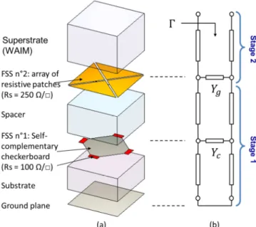
The absorber under study has been designed in the framework of a previous study called SAFAS (Self-complementary surface with low signature) [6], [7]. It is composed of three dielectric layers separated by two FSS, which are located above a ground plane (Fig.1-a).
The permittivity of the initial RF dielectric layers (Superstrate, Spacer, Substrate in Fig.1-a) were 2.2, 2.3 and 4.3 respectively [6]. These RF materials are replaced by structural composite laminates whose composition and associated EM characteristics are given in Table 1. Compared to the previous materials, we note a significant increase of the permittivity for all layers. The loss tangent is also more important for the first two layers but this does not impact the behavior of the absorber.
This absorber can be modeled using an equivalent circuit which is represented in Fig.1-b. Each dielectric layer
2 is associated to a transmission line section and the thin FSS are associated to their admittances.
The equivalent circuits of the first FSS (loaded self-complementary checkerboard) [8] and of the second FSS (array of resistive patches) [9] are given in Fig.2-a, and Fig.2-b respectively. The cascading of the ABCD matrices of each layer allows calculating in a very efficient manner the reflection coefficient of the whole structure [9]. The equivalent model is used to rapidly analyze and optimize the absorber with calculation tools like Matlab. The
optimized result is checked against Full-Wave simulations (CST Microwave Studio) in a second step.
3.
Operating principle
The structure of the absorber can be broken down into two functional stages which are depicted graphically in Fig. 1. The first stage achieves both wideband adaptation and wide-angle stabilization while the second stage further extends the bandwidth.
3.1. First stage analysis
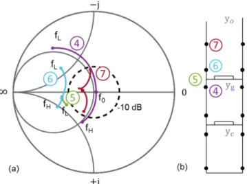
The first stage is composed of a grounded dielectric substrate, a self-complementary checkerboard loaded with resistive elements (FSS n°1), and a dielectric spacer. The total thickness of the first stage is 5.2 mm. The admittance of each layer separately as well as the total admittance of stage 1 are indicated in the admittance Smith chart normalized with respect to free space admittance in Fig. 3. The goal for the matching process is to get as close as possible to the center of the Smith chart.
The admittance of the ground plane plus substrate ① is equivalent to the one of a shunted transmission line. It is thus inductive (upper part of the circle) at low frequency fL and becomes capacitive (lower part of the circle) for high frequency fH. The Smith chart shows that the freestanding loaded self-complementary checkerboard ② is intrinsically wideband as similar to a point in the circle. It is also slightly capacitive, which compensates the inductive component of the shunt at f0. In other terms, the addition of the loaded checkerboard above the grounded substrate enables the point corresponding to f0 to go from inductive behavior in ① to the real axis in ③. The curve is then brought back to the center of the Smith chart ④ by the transmission line (TL) section corresponding to the spacer.
In order to show the benefit of this design, the (mise en Figure 1: (a) Geometry of the unit cell and (b) equivalent
circuit of the EM absorber.
Figure 2: (a) Equivalent circuit of the FSS n°1: self-complementary checkerboard loaded with resistive elements. (b) Equivalent circuit of the FSS n°2: array of resistive patches.
Table 1: EM characteristics of composite layers Layer Superstrate Spacer Substrate Reinforcement Quartz S-glass E-glass
Resin Vinylester Vinylester Polyester Permittivity 3.1 4 4.7 Loss tangent 0.02 0.02 0.02
Figure 3: (a) Admittance of the first stage, layer by layer. The Smith chart is normalized with respect to free space admittance. The circled numbers correspond to the admittances seen at the location marked in (b) : ① is the admittance of the shunt, ② is the admittance of the freestanding FSS, ③ is the complex sum of ① and ②, and ④ is the total admittance of the first stage.
page …) performance of the first stage ④ is compared against classical Salisbury absorbers in Fig. 4. The first Salisbury screen (Fig. 4-a) is composed of an air layer and has a thickness of 5.2 mm. The second Salisbury screen (Fig.4-c) is composed of a dielectric layer whose permittivity is equal to the Spacer layer permittivity ( 4) and it has a thickness of 3 mm. At normal incidence, the SAFASNAV absorber, despite its high permittivity, exhibits a bandwidth very similar to the Salisbury screen bandwidth with air layer (-10 dB between 8 GHz and 17 GHz), and which is much wider than the high permittivity Salisbury screen bandwidth (-10 dB between 10 GHz and 15 GHz). Considering oblique angle of incidence, the Salisbury screen with an air layer exhibits an important frequency shift for increasing angles (approximately 4 GHz at 45°). This shift is limited for the other designs (+500MHz at 45°) due to the
high permittivity dielectric layers. We also see that the increase of the reflection coefficient with respect to the angle is less pronounced for SAFASNAV absorber (-12.5 dB at 45°) than for the two Salisbury screens (-10 dB at 45°).
3.2. Second stage analysis
The second stage is composed of an array of resistive patches realized with a resistive film (FSS n°2) and a dielectric superstrate playing the role of a Wide Angle Impedance Matching (WAIM) layer. The reflection coefficient of each element is represented on the admittance Smith chart in Fig. 5.
The freestanding FSS is capacitive ⑤ which helps to compensate the inductive behavior of stage 1 at low frequency ④, resulting in a curve ⑥ which is almost symmetric with respect to the real axis of the chart. The TL section corresponding to the WAIM dielectric layer rotates curve ⑥ into curve ⑦. Choosing this separation to be approximately λ/4 at the center frequency, we will rotate Figure 4: Reflection coefficient with respect to frequency for various angle of incidence. (a) Salisbury with air layer. (b) First stage of the SAFASNAV absorber. (c) Salisbury with dielectric layer having a permittivity of 4.
Figure 5: (a) Admittance of the second stage, layer by layer. The circled numbers correspond to the reflection coefficient seen at the location marked in (b). ④ is the admittance of stage 1, ⑤ is the admittance of the freestanding resistive patch array, ⑥ is the complex sum of ④ and ⑤, and ⑦ is the total admittance of the second stage.
Figure 6: Reflection coefficient after the first and the second stage of the SAFASNAV absorber.
4 less than 180° at the lower frequency fL and more than ? at the higher frequency fH. The result is the apparition of a loop on the Smith chart, and the frequencies fL, f0, and fH are more clustered together in curve ⑦ than in curve ④. The reflection coefficients of stage 1 and stage 2 (corresponding respectively to ④ and ⑦ on the Smith chart) are finally compared in Fig. 6. We see that the addition of the second stage allows achieving an ultra-wideband response but at the cost of a higher reflection coefficient.
4.
Comparison between structural composite
materials and RF materials
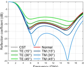
The optimization results () obtained (using Matlab code) after replacement of the dielectric layers by the structural materials are presented in Fig.7 and are validated at normal incidence by comparison with a CST simulation (using the frequency domain solver with Floquet boundary conditions). The analytical model is in very good agreement with the full wave simulation. The total thickness of the absorber is 8.9 mm. The reflection coefficient is less than -14 dB in the 4.6 GHz -17.2 GHz band at normal incidence. At oblique angles of incidence, the reflection coefficient remains under
-10 dB over 5 GHz to 18 GHz, for incidence angles up to 45°.
In order to evaluate the impact of the replacement of the RF dielectric layers by structural composite materials, the results obtained in the initial design are represented in Fig 8. The two designs are showing similar behaviors with respect to the angle of incidence. The reflection coefficient is increased by 4 dB between the initial SAFAS design and SAFASNAV design. Finally, the SAFASNAV design (8.9 mm thickness) is sensibly thinner than the initial SAFAS design (11.5 mm thickness) which is due to the use of high permittivity dielectric substrates.
5.
Conclusions
A metamaterial absorber initially designed for RF materials has been successfully optimized with composite materials. The magnitude of the reflection coefficient is below -14 dB within the frequency band going from 4.6 GHz to 17.2 GHz at normal incidence. It remains under -10 dB within a similar bandwidth considering oblique angles of incidence up to 45°. This study shows that fiber-reinforced composite materials used in combination with frequency selective surfaces can be employed to design a thin and wideband structural absorber.
Acknowledgments
The research leading to these results has received funding by French Ministry of Defense (DGA), through the French National Research Agency (ANR) and Astrid Program in the framework of SAFASNAV project.
References
[1] C. Wang, M. Chen, H. Lei, K. Yao, H. Li, W. Wen, D. Fang, « Radar stealth and mechanical properties of a broadband radar absorbing structure », Compos. Part B
Eng., vol. 123, p. 19-27, August 2017.
[2] W. W. Salisbury, « Absorbent body for electromagnetic waves », US2599944A, 10-June-1952.
[3] L. J. du Toit, « The design of Jaumann absorbers »,
IEEE Antennas Propag. Mag., vol. 36, no 6, p. 17-25, Dec. 1994.
[4] N. Engheta, « Thin absorbing screens using metamaterial surfaces », in IEEE Antennas and
Propagation Society International Symposium (IEEE Cat. No.02CH37313), 2002, vol. 2, p. 392-395.
[5] B. A. Munk, Frequency Selective Surfaces – Theory
and Design. New York: Wiley-Blackwell, 2000.
[6] X. Begaud, S. Varault, A. Lepage, M. Soiron, and A. Barka, « Design of a Thin Ultra Wideband Metamaterial Absorber», Proc. of the 2017 International Conference on Electromagnetics in Advanced Applications (ICEAA), Verona, Italy, 2017
[7] S. Varault, M. Soiron, A. Barka, A. C. Lepage, and X. Begaud, « RCS Reduction With a Dual Polarized Self-Complementary Connected Array Antenna », IEEE
Trans. Antennas Propag., vol. 65, no 2, p. 567-575, Feb. 2017.
Figure 7: Reflection coefficient with respect to frequency for different angles of incidence, using SAFASNAV design.
Figure 8: Reflection coefficient with respect to frequency for different angles of incidence, using initial SAFAS design.
[8] O. Luukkonen, C. Simovski, G. Granet, G. Goussetis, D. Lioubtchenko, A. V. Räisänen and S. A. Tretyakov , « Simple and Accurate Analytical Model of Planar Grids and High-Impedance Surfaces Comprising Metal Strips or Patches », IEEE Trans. Antennas Propag., vol. 56, no 6, p. 1624-1632, June 2008.
[9] X. Begaud, F. Linot, M. Soiron, and C. Renard, « Analytical model of a self-complementary connected antenna array on high impedance surface », Appl. Phys.