Faculty of engineering
Department of electrical engineering and computer science
3D INTEGRATION OF SINGLE ELECTRON
TRANSISTORS IN THE BACK-END-OF-LINE OF 28 nm
CMOS TECHNOLOGY FOR THE DEVELOPMENT OF
ULTRA-LOW POWER SENSORS
INTÉGRATION 3D DE DISPOSITIFS SET DANS LE
BACK-END-OF-LINE EN TECHNOLOGIES CMOS 28 nm
POUR LE DÉVELOPPEMENT DE CAPTEURS ULTRA
BASSE CONSOMMATION
A thesis submitted to Université de Sherbrooke in partial fulfillment of the requirements of the degree of Doctor of Philosophy
Speciality: Electrical Engineering
Yosri AYADI
Jury: Dominique Drouin (Supervisor) Abdelkader Souifi (Supervisor) Serge Ecoffey
Andreas Ruediger Stéphane Monfray
i
Acknowledgments
First, I would like to express my deepest sense of gratitude to my supervisors Prof. Dominique Drouin and Prof. Abdelkader Souifi for providing me the opportunity to undertake such exciting and challenging Ph.D. research project in such a fascinating field of nanoelectronics. My deepest thanks also go to associate Prof. Serge Ecoffey for supervising the research project work. I am grateful to all of them for the encouragement, support, guidance, advices, and enriching discussions. I owe to them all I have learned throughout this “adventure”. A Special thanks to my supervisor Prof. Dominique Drouin for believing in me and giving me the chance to go further in my research project.
I would like to thank all the nanoelectronics research group members for the support, the collaborative and constructive work, being helpful and providing a lovely and friendly ambiance, which made it more convenient to carry out the research project. In particular, Bruno Lee Sang and Gabriel Droulers for all the help rendered in various ways and the enriching discussions. I acknowledge the help from Jean-Philippe Richard, Fréderic Bourque and Marc Guilmain. A special thanks to Pascal Lemieux for helping with the development of the FD-SOI FET simulator. His amazing skills in programming and keen interest account for a big part of the developed simulator.
I am grateful to all the collaborators and project partners, Jean-Pierre Cloarec, Stéphane Monfray, Adranik Sarkissian, Andreas Rudiger, Bertrand Villequin and Jonathan Genest who generously shared their insights and expertize. Their valuable and meticulous criticism and suggestions were very helpful and constructive, and account for a big part of the achieved work. I would like to thank the entire 3IT-LNN, 3IT-LCSM and IMDQ technical and research staff for their support and being always ready to give a hand, in particular Pierre Langlois, Marie-José Gour, Étienne Paradis, Carolyn Roy, Denis Pellé, Daniel Blackburn, René Labrecque, Christian Sara-Bournet and Michael Lacerte for their tremendous help, favours and moral support.
I would like to thank all the INL members for the great time spent with them. A special thanks to Annie Suslec, Yvan Doyeux, Nicolas Baboux, Lama Rahal, Francis Calmon Daniel Barbier,
ii Acknowledgments Brice Gautier and Christian Gontrand for their kindness, all kinds of support, the coffee breaks, and the very special discussions and jokes!
I would like to thank all the 3IT members, for taking part of this project and all the moments shared together. A special thanks to Osvaldo Arenas and Martine Parent for the moral support, and Arnaud Samson for the help with LabView programming.
I am so grateful to La Fondation Force for the support and making this project go to his end. I owe everything to my parents who never kept sacrificing and dedicating themselves to my accomplishment so trustworthy and humbly and without any expectation whatever. A mere “thank you” to acknowledge their sacrifice can hardly do justice to the immerse gratitude I feel. I hope my accomplishments can make them proud. Last, I am so grateful to all the people who took part in this “adventure”, inspired me, supported me and fed me with food, compassion and love. I owe to them a LOT. I could not have made it this far without their constant moral support and encouragement. I am grateful to Sylvie Jacques, Hatem Laabidi, Véronique Thibaut, Tina Merz, Frances Alvo, Samuel Paquette, Simon Stankovich, Joanna Bateman, Dany Loubier, Philippe Demers, Dominique Boiverts, Julia Goolia, Geneviève Kiliko, Rafael Soler Hernandez, Maricarmen Soler Hernandez, Matteo Vignetti and Daniel Thomas for all what they have done for me.
iv
Abstract
The need of integration of new functionalities on mobile and autonomous electronic systems has to take into account all the problematic of heterogeneity together with energy consumption and thermal dissipation. In this context, all the sensing or memory components added to the CMOS (Complementary Metal Oxide Semiconductor) processing units have to respect drastic supply energy requirements.
Smart mobile systems already incorporate a large number of embedded sensing components such as accelerometers, temperature sensors and infrared detectors. However, up to now, chemical sensors have not been fully integrated in compact systems on chips. Integration of gas sensors is limited since most used and reliable gas sensors, semiconducting metal oxide resistors and catalytic metal oxide semiconductor- field effect transistors (MOSFETs), are generally operated at high temperatures, 200–500 °C and 140–200° C, respectively.
The suspended gate-field effect transistor (SG-FET)-based gas sensors offer advantages of detecting chemisorbed, as well as physisorbed gas molecules and to operate at room temperature or slightly above it. However they present integration limitations due to the implementation of a suspended gate electrode and augmented channel width in order to overcome poor transconductance due to the very low capacitance across the airgap.
Double gate-transistors are of great interest for FET-based gas sensing since one functionalized gate would be dedicated for capacitively coupling of gas induced charges and the other one is used to bias the transistor, without need of airgap structure. This work discusses the integration of double gate-transistors with CMOS devices for highly sensitive and ultra-low power gas sensing applications.
The use of single electron transistors (SETs) is of great interest for gas sensing applications because of their key properties, which are its ultra-high charge sensitivity and the ultra-low power consumption and dissipation, inherent to the fundamental of their operation based on the transport of a reduced number of charges.
Therefore, the work presented in this thesis is focused on the proof of concept of 3D monolithic integration of SETs on CMOS technology for high sensitivity and ultra-low power gas sensing functionality. The proposed approach is to integrate metallic double gate-single electron
transistors (DG-SETs) in the Back-End-Of-Line (BEOL) of CMOS circuits (within the CMOS interconnect layers) using the nanodamascene process. We take advantage of the hyper sensitivity of the SET to electric charges as well from CMOS circuits for high-speed signal processing.
Fully depleted-silicon on insulator (FD-SOI) MOSFETs are very attractive devices for gas sensing due to their amplification capability when operated in the sub-threshold regime which is the strongest asset of these devices with respect to the FET-based gas sensor technology. In addition these devices are of a high interest in terms of integration density due to their small size. Moreover FD-SOI FETs is a mature and well-modelled technology. We focus on the functionalization of the front gate of a FD-SOI MOSFET as a demonstration of the DG-transistor-based gas sensor.
Kelvin probe has been the privileged technique for the investigation of FET-based gas sensors’ sensitive material via measuring the work function variation induced by gas species adsorption. In this work an alternative technique to investigate gas sensitivity of materials suitable for implementation in DG-FET-based gas sensors, based on measurement of the surface charge induced by gas species adsorption is discussed.
In order to increase the specific surface of the sensing electrode, a novel concept of functionalized gate surface texturing suitable for FET-based gas sensors are presented. It is based on the spray coating of a multi-walled-carbon nanotubes (MW-CNTs) suspension to deposit a MW-CNT porous network as a conducting frame for the sensing material.
The main objective of this Ph.D. thesis can be divided into 4 parts: (1) modelling and simulation of a DG-SET and a FD-SOI MOSFET-based gas sensor response, and estimation of the sensitivity as well as the power consumption; (2) investigation of Pt sensitivity to hydrogen by surface charge measurement technique and development of the sensing electrode surface texturing process with CNT networks; (3) development and optimization of the DG-SET integration process in the BEOL of a CMOS substrate, and (4) FD-SOI MOSFET functionalization with Pt for H2 sensing.
Keywords: Single electron transistors, 3D monolithic integration, FET-based gas sensors, Gas
sensing, Hydrogen detection, Sensing layer texturing, MW-CNT networks, Ultra-low power, FDSOI.
vii
Résumé
La forte demande et le besoin d’intégration hétérogène de nouvelles fonctionnalités dans les systèmes mobiles et autonomes, tels que les mémoires, capteurs, et interfaces de communication doit prendre en compte les problématiques d’hétérogénéité, de consommation d’énergie et de dissipation de chaleur.
Les systèmes mobiles intelligents sont déjà dotés de plusieurs composants de type capteur comme les accéléromètres, les thermomètres et les détecteurs infrarouge. Cependant, jusqu’à aujourd’hui l’intégration de capteurs chimiques dans des systèmes compacts sur puce reste limitée pour des raisons de consommation d’énergie et dissipation de chaleur principalement. La technologie actuelle et fiable des capteurs de gaz, les résistors à base d’oxyde métallique et les MOSFETs (Metal Oxide Semiconductor- Field Effect Transistors) catalytiques sont opérés à de hautes températures de 200–500 °C et 140–200 °C, respectivement.
Les transistors à effet de champ à grille suspendu (SG-FETs pour Suspended Gate-Field Effect Transistors) offrent l’avantage d’être sensibles aux molécules gazeuses adsorbées aussi bien par chemisorption que par physisorption, et sont opérés à température ambiante ou légèrement au-dessus. Cependant l’intégration de ce type de composant est problématique due au besoin d’implémenter une grille suspendue et l’élargissement de la largeur du canal pour compenser la détérioration de la transconductance due à la faible capacité à travers le gap d’air.
Les transistors à double grilles sont d’un grand intérêt pour les applications de détection de gaz, car une des deux grilles est fonctionnalisée et permet de coupler capacitivement au canal les charges induites par l’adsorption des molécules gazeuses cibles, et l’autre grille est utilisée pour le contrôle du point d’opération du transistor sans avoir besoin d’une structure suspendue. Les transistors monoélectroniques (les SETs pour Single Electron Transistors) présentent une solution très prometteuse grâce à leur faible puissance liée à leur principe de fonctionnement basé sur le transport d’un nombre réduit d’électrons et leur faible niveau de courant.
Le travail présenté dans cette thèse fut donc concentré sur la démonstration de l’intégration 3D monolithique de SETs sur un substrat de technologie CMOS (Complementary Metal Oxide Semiconductor) pour la réalisation de la fonction capteurs de gaz très sensible et ultra basse consommation d’énergie. L’approche proposée consiste à l’intégration de SETs métalliques à
Résumé viii
double grilles dans l’unité de fabrication finale BEOL (Back-End-Of-Line) d’une technologie CMOS à l’aide du procédé nanodamascene. Le système sur puce profitera de la très élevée sensibilité à la charge électrique du transistor monoélectronique, ainsi que le traitement de signal et des données à haute vitesse en utilisant une technologie de pointe CMOS disponible.
Les MOSFETs issus de la technologie FD-SOI (Fully Depleted-Silicon On Insulator) sont une solution très attractive à cause de leur pouvoir d’amplification du signal quand ils sont opérés dans le régime sous-le-seuil. Ces dispositifs permettent une très haute densité d’intégration due à leurs dimensions nanométriques et sont une technologie bien mature et modélisée. Ce travail se concentre sur le développement d’un procédé de fonctionnalisation d’un MOSFET FD-SOI comme démonstration du concept du capteur de gaz à base de transistor à double grilles. La sonde Kelvin a été la technique privilégiée pour la caractérisation des matériaux sensibles par le biais de mesure de la variation du travail de sortie induite par l’adsorption de molécules de gaz. Dans ce travail, une technique de caractérisation des matériaux sensibles alternative basée sur la mesure de la charge de surface est discutée.
Pour augmenter la surface spécifique de l’électrode sensible, un nouveau concept de texturation de surface est présenté. Le procédé est basé sur le dépôt de réseaux de nanotubes de carbone multi-parois par pulvérisation d’une suspension de ces nanotubes. Les réseaux déposés servent de «squelettes» pour le matériau sensible.
L’objectif principal de cette thèse de doctorat peut être divisé en 4 parties : (1) la modélisation et simulation de la réponse d’un capteur de gaz à base de SET à double grilles ou d’un MOSFET FD-SOI, et l’estimation de la sensibilité ainsi que la puissance consommée; (2) la caractérisation de la sensibilité du Pt comme couche sensible pour la détection du H2 par la technique de mesure
de charge de surface, et le développement du procédé de texturation de surface de la grille fonctionnalisée avec les réseaux de nanotubes de carbone; (3) le développement et l’optimisation du procédé de fabrication des SETs à double grilles dans l’entité BEOL d’un substrat CMOS; et (4) la fonctionnalisation d’un MOSFET FD-SOI avec du Pt pour réaliser la fonction de capteur de H2.
Mots-clès : Transistors monoélectroniques, Intégration 3D monolithique, Capteur de gaz à
base de FET, Capteur de gaz, Détection du dihydrogène, Texturation de surface de la couche sensible, Réseaux de MW-CNTs, Ultra-basse consommation, FDSOI.
x
Table of contents
Acknowledgments ... i Abstract ... iv Résumé ... vii Table of contents ... xList of Figures ... xiv
List of Tables ... xxiv
List of Acronyms ... xxv
List of Symbols ... xxix
CHAPTER 1 Introduction ... 1
1.1 General ... 1
1.2 Gas sensor integration challenges ... 1
1.3 Emergence of low power transistors ... 2
1.4 Open questions and research project objectives ... 3
1.5 Outline of this thesis ... 6
CHAPTER 2 Literature review on integrated gas sensors ... 8
2.1 Introduction ... 8
2.2 Sensing materials ... 10
2.3 Gas adsorption/desorption on solids ... 11
2.4 Conductivity gas sensors ... 13
2.5 Metal oxide gas sensors ... 17
2.5.1 Sensing mechanism ... 17
2.5.2 Sensing influencing factors ... 23
2.5.2.b Operating temperature ... 24
2.6 Field effect transistor-based gas sensors ... 27
2.6.1 MOSFET gas sensors (Catalytic MOSFETs) ... 28
2.6.2 SG-FET-based gas sensors ... 33
2.7 CNT and graphene-based gas sensors ... 37
2.8 Single electron transistor-based gas sensor ... 42
2.9 Conclusion ... 44
CHAPTER 3 Device design, modelling and simulation ... 46
3.1 Introduction ... 46
3.2 SET theory ... 47
3.2.1 Coulomb blockade effect ... 47
3.2.2 Single electron transistor ... 54
3.2.3 The Orthodox theory ... 59
3.3 Double gate transistor-based gas sensor ... 60
3.4 DG-SET-based gas sensor design, modelling and simulation ... 67
3.4.1 Functionalized Gate Capacitances Calculation ... 68
3.4.2 DG-SET-based gas sensor response simulation ... 81
3.5 FD-SOI MOSFET-based gas sensor modelling and simulation ... 88
3.5.1 UTBB FD-SOI MOSFET model ... 89
3.5.2 UTBB FD-SOI MOSFET-based gas sensor response simulation ... 90
3.6 Conclusion ... 94
CHAPTER 4 Top-gate functionalization ... 97
4.1 Introduction ... 97
Table of Contents xii
4.2.1 Pt interactions with hydrogen and oxygen ... 99
4.2.2 Pt as a sensing layer for H2 ... 101
4.3 Sensing electrode surface texturing with CNT networks ... 103
4.3.1 Surface texturing using MW-CNTs concept ... 105
4.3.2 MW-CNTs dispersion ... 105
4.3.3 MW-CNT Spray coating process ... 107
4.3.4 Pt-coated MW-CNT networks ... 116
4.4 Material sensitivity characterization ... 117
4.4.1 Kelvin probe technique ... 117
4.4.2 Surface charge measurement technique ... 118
4.4.2.a Surface charge measurement principle ... 118
4.4.2.b Experimental set-up and measurement conditions ... 120
4.4.2.c Sample design and fabrication process ... 122
4.5 Platinum sensitivity to H2 ... 126
4.6 H2 Sensing surface sizing for integration with a DG-transistor ... 136
4.6.1 H2 Sensing with a DG-SET ... 136
4.6.2 H2 Sensing with a DG-FET ... 137
4.7 Conclusion ... 140
CHAPTER 5 Gas sensor integration and electrical characterization ... 143
5.1 Introduction ... 143
5.2 DG-SET integration ... 143
5.2.1 The nanodamascene process ... 143
5.2.2 Fabrication process ... 146
5.2.2.b E-beam lithography layout ... 155
5.2.3 Fabrication process optimization ... 159
5.2.3.a Tunnel junction dielectric ... 159
5.2.3.b Chemical mechanical planarization process ... 160
5.3 FD-SOI MOSFET gate functionalization ... 172
5.4 Nano device electrical characterization ... 176
5.5 Conclusion ... 179
CHAPTER 6 Conclusions and perspectives ... 181
6.1 Summary and conclusions ... 181
6.2 Perspectives ... 183
APPENDIX A Simulated FD-SOI MOSFET model ... 186
A.1 UTBB FD-SOI MOSFET model ... 186
A.2 Simulated UTBB FD-SOI MOSFET characteristics ... 193
APPENDIX B Surface charge measurement technique ... 196
B.1 Measurement instrument ... 196
B.2 Experimental set-up ... 199
APPENDIX C Sensing material characterization by work function measurements ... 201
C.1 Kelvin probe measurement principle ... 201
C.2 Sensing material work function change measurements ... 202
APPENDIX D UV lithography layout of nanodamascene SETs ... 205
xiv
List of Figures
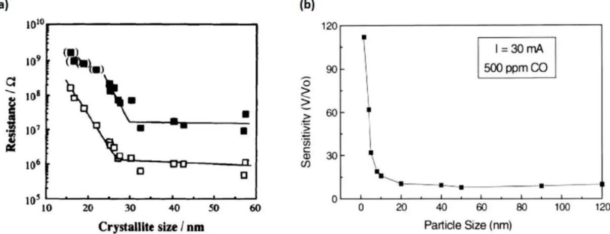
Figure 1.1 Concept of 3D SET-CMOS Integrated Circuits and Sensors [1]…….… 4 Figure 1.2 3D schematic representation of a SET embedded in a dielectric layer fabricated by the nanodamascene process. .………. 5 Figure 1.3 3D schematic representation of the proposed concept of a fully integrated metallic SET gas sensor on a CMOS substrate. ………... 6 Figure 2.1 Different types of gas sensors. .………...………. 9 Figure 2.2 Typical structure of a conductivity gas sensor. Reproduced from [2]. … 13 Figure 2.3 Typical Structure of a metal oxide gas sensor. Reproduced from [3]. ..…. 15 Figure 2.4 Metal oxide gas sensor based on a micromachined hotplate on a Si substrate. Reproduced from [4]. ..……….... 16 Figure 2.5 Diagram of band bending after chemisorption of charged species (here the ionosorption of oxygen) , , and denote the energy of the conduction band, valence band, and the Fermi level, respectively, while Λ denotes the thickness of the space-charge layer, and denotes the potential barrier. Reproduced from [5]. 18 Figure 2.6 Schematic of a compact sensing layer with geometry and energy band diagrams; is the thickness of the depleted surface layer; is the layer thickness and the band bending energy barrier height. a) Represents a partly depleted compact layer (“thicker”), and b) represents a completely depleted layer (“thinner”). Reproduced from [6]. …………..……….……..………. 20 Figure 2.7 Schematic representation of a porous sensing layer with geometry and surface energy band-case with necks between grains. is the neck diameter; is the thickness of the depletion layer. a) Represents the case of only partially depleted necks whereas b) represents large grains where the neck contact is completely depleted. Reproduced from [6]. …..………. 21 Figure 2.8 Schematic representation of a porous sensing layer with geometry and energy band. is the Debye length and is the grain size. Reproduced from [6]. ..…. 22 Figure 2.9 a) Resistance variation as a function of WO3 crystallite size for; □ air
and ■ 5ppm NO2 at 300 °C. Reproduced from [7]. b) Sensitivity versus grain size of a
SnO2 nanocrystals-based sensor under exposure to 500 ppm. Reproduced from [8]. … 24
Figure 2.10 Sensitivity- temperature profile of chemoresistors with undoped, Pt-doped, Pd-doped and Ag-doped SnO2 to 0.8% of H2, 0.5% of CH4, 0.2% of C3H8 and
0.02% of CO in air. The sensitivity is defined as the ratio of sensor conductance in the presence of a target gas to the conductance in air (mixture of O2 and N2). Reproduced
from [9]. ……….…………. 25 Figure 2.11 Sensitivity-operating temperature profile of a) ZnO nanoplate-based chemoresistor at 100 ppm of ethanol and chlorobenzene. Reproduced from [5]. b) Screen printed WO3 thick layer resistor sintered at different temperatures at 100 ppm
of NO2.Reproduced from [10]. c) Undoped and Pt-doped SnO2 thin layer chemoresistor
at 180 ppm of CO. Reproduced from [11]. d) Screen printed ZnO thick film with different RuO2 doping percentage. Reproduced from [7]. .……..……….………. 25
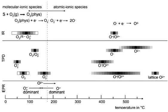
Figure 2.12 Literature survey of oxygen species detected at different temperatures at SnO2 surfaces with IR analysis, TPD and EPR (electron paramagnetic resonance). Reproduced from [6]. ………..………..…………. 27
Figure 2.13 Schematic view of a) a SG-FET, b) a Pd-MOSFET. Reproduced from [12]. ………...……….……….… 28 Figure 2.14 Cross sectional schematic of an n-channel MOSFET gas sensor structure with a catalytic metal gate electrode. Adapted from [13]. ……… 29 Figure 2.15 Change in threshold voltage with time in two different gas mixtures at a temperature of 150 °C. Reproduced from [14]. ……… 29 Figure 2.16 Transduction principle in catalytic MOSFET. a) versus curve under and without exposure to H2. b) Schematic illustrating the work function change
of the inner Pd surface due to the trapped hydrogen atom at the Pd-SiO2 interface. ….. 31
Figure 2.17 Schematic cross-sectional view of the low-power MOSFET array gas sensor. The electronic components are located in a silicon island isolated from the silicon chip frame by a dielectric membrane made of two nitride layers. Reproduced from [15]. ...……….………. 33 Figure 2.18 Cross sectional schematic of n-channel SGSFET gas sensor. Adapted from [13]. ……….……….………. 34 Figure 2.19 a) Schematic representation of Lundström -FET/SG-FET double sensor in CMOS technology. b) Different hydrogen sensitivity of Lundström -FET and SG-FET with Pt gate at low H2 concentrations. c) Cross sensitivity of the double sensor
system to a 100 ppm CO pulse, compared to the system’s reaction to a 50 ppm-hydrogen flow. Calibrated work function change at the sensing layer is shown. Reproduced from [16]. ………..……..……… 36 Figure 2.20 Changes in resistivity caused by graphene exposure to various gases diluted in concentration to 1 ppm. The positive (negative) sign of changes is chosen here to indicate electron (hole) doping. Region I: the device is in a vacuum before its exposure; II: exposure to a 5 l volume of a diluted chemical; III: evacuation of the experimental set-up; and IV: annealing at 150 °C. Reproduced from [17]. ……….. 38 Figure 2.21 Schematic of a typical CNT-FET structure. The Si substrate acts as a back gate. Adapted from [18]. .………. 39 Figure 2.22 Chemical gating effects to the semiconducting SWNT. Current versus gate voltage curves before NO2, after NO2 and after NH3 exposures. The measurements
were carried out successively after sample recovery and with exposure to NH3 (0.1–
1%) and NO2 (2–200 ppm) in an air flow rate of 700 ml/min. The channel length was
around 5μm. Reproduced from [19]. ……… 40 Figure 2.23 Schematic of the two CNT-FET structures used by Liu et al.. (a) Contact exposed device. (b) Centre exposed device. Reproduced from [20]. ………… 40 Figure 2.24 - curves of a) a contact-exposed device and b) a centre-exposed device under exposure to different concentrations of NO2 and NH3. Reproduced from
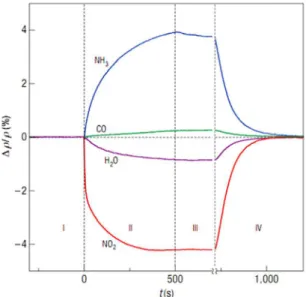
[20]. .………...….……… 41 Figure 2.25 a) Time response of SET-based gas sensor to the injection of the mixture of gases into the flow cell. The NO2 concentration is 41% in N2. b) Variation of the
drop in drain current in function of concentration of NO2 in N2. Reproduced from [21]. 43
Figure 2.26 Proposed ionosorption mechanism resulting in charge transfer in the SET gas sensor. Reproduced from [21]. .……….. 44 Figure 3.1 The single-island, double tunnel junction system. a) Schematic structure of single-island, double tunnel junction system showing an isolated nano-sized metallic island placed close to two metallic electrodes: drain and source. b) Circuit diagram of
List of Figures xvi
a single-island, double tunnel junction system. and are respectively island-to-source tunnel junction capacitance and resistance. and are respectively island-to-drain capacitance and resistance. .………..………. 48 Figure 3.2 a)Schematic representation of the single-island, double tunnel junction system with drain and source electrically connected. b) Circuit diagram of the single-island, double tunnel junction system with drain and source electrically connected. … 49 Figure 3.3 a)Schematic representation of the single-island, double tunnel junction system where a voltage is applied between drain and source. b) Circuit diagram of the single-island, double tunnel junction system where a voltage is applied between source and drain. ...……….……….. 51 Figure 3.4 Energy band diagram of a single-island, double tunnel junction system when is null, showing possible island discrete levels relative to the island and drain Fermi levels corresponding to the island net charge = × , where is the elementary charge and is an integer. ………. 51 Figure 3.5 - characteristics corresponding to a symmetrical single-island, double tunnel junction system, with energy band diagrams corresponding to distinct values of . Represented island discrete energy levels correspond to the island net charge = × , where is the elementary charge and is an integer. Since the tunnel junctions are symmetrical, these levels are at the same gap from the island Fermi level corresponding to neutral island charge. ……….. 52 Figure 3.6 a) Schematic structure of a single electron transistor. b) Circuit diagram of a single electron transistor. The source is considered as common voltage reference for gate and drain polarization. denotes the gate-to-island capacitance. ……….. 54 Figure 3.7 a) - characteristics at a small , known as Coulomb oscillations. b) Number of electrons accumulated in the island as a function of . c-f) Energy band diagrams corresponding to distinct values of at a small for = 0 , =
, < < and = . ……… 56
Figure 3.8 I - characteristics of a SET in the “ON” and “OFF” states. (This
characteristic corresponds to symmetrical tunnel junction SET, symmetrical
polarization, and a null background island charge). ……… 57 Figure 3.9 Coulomb diamonds of a SET. a) Conduction stability diagram. Numbers separated by commas represent the possible states in terms of the number of electrons charging the island. Black coloured regions are Coulomb blockade zones [22]. b) Illustration of SET parameters defining the shape of the Coulomb diamonds. ………. 58 Figure 3.10 Schematic representation of gas molecules chemisorption on a sensing layer surface showing the partial charge transfer. a) H2 chemisorption on Pt surface
showing the partial electron transfer. b) O2 chemisorption on SnO2 surface showing the
partial electron withdrawing. ………...……… 62 Figure 3.11 a)3D schematic of the DG-SET-based gas sensor concept showing the top gate connected to the sensing pad and playing the role of the functionalized gate and the side gate serving as a bias gate. b) Circuit diagram of the DG-SET-based gas sensor showing the island capacitively coupled to two different gate electrodes: a functionalized gate and a bias gate. and denote respectively functionalized gate and bias gate capacitances. Only the bias gate is polarized by the voltage source . … 63 Figure 3.12 Coulomb oscillations with respect to the functionalized gate charge for
Figure 3.13 3D schematic representation of the FD-SOI MOSFET-based gas sensor concept showing the front gate connected to the sensing pad and playing the role of the functionalized gate and the substrate serving as a control gate. ……… 66 Figure 3.14 Typical characteristics / at various of an n-type FD-SOI MOSFET showing the shifting effect of the back biasing. ……… 66 Figure 3.15 Circuit diagram of a DG –SET showing the functionalized gate parasitic capacitances , and , and bias gate parasitic capacitances and . ……… 67 Figure 3.16 Functionalized gate 3D scheme showing all the capacitances at play in the DG-SET characteristics. The functionalized gate is implemented as a top-gate, and the bias gate as a side-gate. ……….. 70 Figure 3.17 3D Schematic of the simulated DG-DET showing the geometrical parameters. ………...………... 71 Figure 3.18 Impact of top gate side length on top gate capacitances. a) Top gate capacitances versus side length for = 50 nm. b) versus side length for
= 50 nm. ………. 73 Figure 3.19 Impact of top gate distance on top gate capacitances. a) Top gate capacitances versus top gate distance for = 30 nm. b) versus top gate distance for
= 30 nm. ………...……….. 74 Figure 3.20 The ratio as a function of side length for = 15 nm. ……… 76 Figure 3.21 Top gate misalignment along XX’ and YY’ axis. Δ and Δ denote the top gate deviation respectively along XX’ and YY’ axis. ……… 78 Figure 3.22 Impact of misalignment along XX’ on top gate capacitances for
= 15 nm and = 20 nm. a) Top gate-to-island and top gate total parasitic capacitances versus misalignment along XX’ axis. b) versus misalignment along XX axis’. ………..………. 79 Figure 3.23 Impact of misalignment along YY’ on top gate capacitances for
= 15 nm and = 20 nm. a) Top gate-to-island and top gate total parasitic capacitances versus misalignment along YY’ axis. b) versus misalignment along YY’ axis. ………...……….. 80 Figure 3.24 Circuit diagram of simulated DG-SET model without parasitic capacitances. The functionalized gate electrode is a “non-volatile node” with a pre-set background charge. The source is taken as a common voltage reference for bias gate and drain polarization. ………. 83 Figure 3.25 a) Simulated Coulomb diamonds of the DG-SET model without parasitic capacitances at 10 K and for null charge on the functionalized gate, from
which line traces in b) and c) were extracted. ……….……… 83 Figure 3.26 a) Simulated Coulomb diamonds of the DG-SET model without
parasitic capacitances at 300 K and for null charge on the functionalized gate, from which line traces in b) and c) were extracted. ………….……… 84 Figure 3.27 Circuit diagram of simulated DG-SET model with all the parasitic capacitances. The functionalized gate electrode is a “non-volatile node” with a pre-set background charge. The source is taken as a common voltage reference for bias gate and drain polarization. ………..……….. 85 Figure 3.28 a) Simulated Coulomb diamonds of the DG-SET model with all the parasitic capacitances at 10 K and for a null charge on the functionalized gate, from which traces in b) and c) were extracted. ………. 86
List of Figures xviii
Figure 3.29 a) Simulated Coulomb diamonds of the DG-SET model with all the parasitic capacitances at 300 K, and for a null charge on the functionalized gate, from which traces in b) and c) were extracted. ………. 87 Figure 3.30 at varying functionalized gate charge simulated for the DG-SET model with all the parasitic capacitances at 300 K. ……….. 88 Figure 3.31 Simulated for = 0.1 V, = 30 nm and = 0.5 μm, with back bias voltages varying from -3 to +3 V. ……… 91 Figure 3.32 Simulated curves for = 0.1 V, = 2 V, and = 0.5 μm with varying the channel length from 20 to 40 nm. ………. 92 Figure 3.33 Extracted sensitivities at varying channel length for = 0.1 V, = 2 V, and = 0.5 μm. ………..……….. 92 Figure 3.34 Simulated curves for = 0.1 V, = 2 V, and = 30 with varying the channel length from 100 to 500 nm. ……… 93 Figure 3.35 Simulated curves for = 0.1 V, = 2 V, and channel parameters = 30 nm, = 0.5 μm, with varying operating temperature. …. 94 Figure 4.1 Cross section schematic of a DG-FET-based gas sensor realized with an FD-SOI MOSFET showing the sensing pad connected directly to the front gate of the transistor. Adapted from [23]. ………. 98 Figure 4.2 Schematic representation of hydrogen and oxygen molecules adsorption on Pt surfaces showing a partial charge transfer. a) H2 dissociative chemisorption on Pt
surface showing a partial electron transfer. b) O2 dissociative chemisorption on Pt
surface showing a partial electron withdrawing. ……… 100 Figure 4.3 Pt-SG-FET sensitivity to H2 at 30 °C. a) Pt-SG-FET response signal to
0.1% H2 at 30 °C and 0% RH. b) H2 concentration dependence of the Pt-SG-FET
response at 30 °C and 0% RH. Reproduced from [24]. ……… 102 Figure 4.4 a) Response as a function of hydrogen concentration at 100 °C in synthetic air of the Pd Lundström-FET and the Pt-SG-FET. b) Cross section schematic of the combined Pd Lundström-FET/ Pt-SG-FET sensor system. c) Top view image of the sensor chip with the combined Pd Lundström-FET/ Pt-SG-FET devices. Reproduced from [16]. ………. 102 Figure 4.5 a) Pt surface work function change under exposure to 2% H2 in synthetic
air at 30% RH and different temperatures. b) The drift behaviour of Pt work function in hydrogen containing air with 30% RH at 75 °C. Reproduced from [12]. ……… 103 Figure 4.6 3D schematic representations of carbon nanomaterials. a) A sheet of graphene. Reproduced from [25]. b) A single-walled CNT. Reproduced from [26]. .… 104 Figure 4.7 CNT dispersion process. a) CNT powder is added to the solvent in a falcon tube. b) The dispersion is sonicated using a sonicator probe. Inset: a close up of the sonicator probe into the CNT solution c) A homogenous suspension is obtained after sonicating. ………...……… 107 Figure 4.8 Spray coating system. a) A photograph of the model Prism BT spray coating system from Ultrasonic Systems, Inc [27]. b) 3D schematic of the ultrasonic spray head [27]. c) 3D schematic of the spray coating process. ……… 108 Figure 4.9 The “coffee-ring effect”. a) SEM image of MW-CNTs coating on a 5 nm/50 nm-thick Cr/Au bilayer showing the concentrated CNTs in ring-shaped regions highlighted in yellow. b) A close-up of the “coffee-ring effect”. c) A close-up of the region inside the “ring”. Inset: a close-up of the deposited MW-CNT networks. d) A
close-up of the region outside the “ring” showing the lack of CNT-network deposition (see text for coating details). ……… 110 Figure 4.10 SEM image of CNT deposition by a single line pattern spray coating of a 0.1 mg/ml-concentrated MW-CNT dispersion in NMP at 40 mm/s of speed, 0.5 ml/min of flow rate and temperature of 70 °C. ……… 110 Figure 4.11 SEM images of CNT deposition by alternated perpendicular lines coating pattern repeated subsequently 20 times using a 0.05 mg/ml-concentrated MW-CNT dispersion in NMP at 40 mm/s of speed, 0.25 ml/min of flow rate and temperature of (a) 150 °C and (b) 230 °C. ……… 111 Figure 4.12 SEM images of MW-CNT networks layers obtained by spray coating at the optimized parameters for a) 10, b) 20, c) 50, d) 150 and 300 iterations, showing uniform distribution of CNT deposition. ………. 113 Figure 4.13 SEM images of MW-CNT networks layers obtained by spray coating at the optimized parameters for a) 10, b) 20, c) 50, d) 150 and 300 iterations, showing surface coverage. ……… 113 Figure 4.14 SEM image of porous CNT networks layer obtained by spray coating at the optimized parameters for 150 iterations. Inset: a close up of the CNT mat showing CNTs overlapped yielding a porous layer. ……….. 114 Figure 4.15 Topography scan of a porous CNT layer obtained by spray coating for 300 iterations. ………..… 114 Figure 4.16 a) Schematic illustration of profilometer line trace of the step obtained by spray coating a sample with a masked region, offering a reliable estimation of the CNT layer thickness. b) Profilometer trace of the step of a sample from batch E (coating at 300 iterations). Levelling is done on the Au trace. ……… 115 Figure 4.17 SEM images of MW-CNT networks layers obtained by spray coating at the optimized parameters for a) 10, b) 20, c) 50, d) 150 and 300 iterations, after 50 nm-thick Pt layer evaporation, showing conformal coating of the nanotubes. ……… 117 Figure 4.18 SEM images of MW-CNT networks layers obtained by spray coating at the optimized parameters for 150 iterations, after (a) 50 nm and (b) 5 nm -thick Pt layer evaporation showing the good wettability of the MW-CNTs by Pt. ……… 117 Figure 4.20 Schematic representation of surface charge measurement configuration and equivalent circuit diagram of the electrometer with feedback amplifier in Coulombs mode. , and are respectively the input capacitance, the source capacitance and the electrometer reference feedback capacitance. is the open loop gain of the electrometer operation amplifier. ……… 119 Figure 4.21 Schematic of equivalent system of a sensing layer connected to an electrometer (with feedback amplifier) in Coulombs mode in surface charge measurement configuration illustrated for a) H2 detection with Pt, b) CO detection with
SnO2, c) and oxygen detection with Pt, and yielded charge reading change shown in d)
and e). Charges in green or red are meant to respectively appear or disappear as a result of the detection event. ……….. 120 Figure 4.22 Schematic representation of the experimental set-up used in surface charge measurements. ……….. 121 Figure 4.23 A view of the gas chamber and the sample holder. a) Photograph of the metallic chamber with the sample placed inside. b) Bottom view photograph of a sample wirebonded to a chip carrier and mounted on the sample holder with the flexible 121
List of Figures xx
heater. c) Top view photograph of a sample mounted on a chip holder with the flexible heater. ……….. Figure 4.24 Sample design used in gas-sensitive material characterization using surface charge measurement technique. a) Top view and b) cross-section schematic representation of sample structure. ……….. 122 Figure 4.25 UV lithography layout of a cell. Right: a close-up of an alignment mark. 123 Figure 4.26 Schematic of sample fabrication process flow. ……… 124 Figure 4.27 Schematic of CNT-textured sample fabrication process flow. ………… 126 Figure 4.28 Pt layer charge variation response at varying temperature from 80 to 190 °C to oxygen concentration of 20% in pure nitrogen. ………. 127 Figure 4.29 Time response of platinum layer to the injection of 20% O2 in pure N2
at 130 °C. ………. 128 Figure 4.30 Time response of a platinum layer to the injection of 0.5% H2 in
synthetic air at 130 °C. ……… 129 Figure 4.31 Time response of platinum layer to the injection of 4% H2 in synthetic
air at 60 °C. ……….. 130 Figure 4.32 Hydrogen concentration dependence of platinum layer response in term of charge reading variation at 60 °C in the linear (a) and semi-logarithmic scale (b). …. 131 Figure 4.33 Plot of 1 ∆ ⁄ versus / at 60 °C. ……… 134 Figure 4.34 Pt layer charge variation response at varying temperature from 80 to 190 °C to hydrogen concentration of 4% in synthetic air. ……….. 135 Figure 4.35 Hydrogen concentration dependence of platinum layer response in term of charge reading variation at 130 °C in synthetic air. ………. 135 Figure 4.36 Pt-functionalized DG-SET-based H2 sensor response to varying
concentration. ………...………... 137 Figure 4.37 Pt-functionalized DG-FET-based H2 sensor response to varying H2
concentration. ………...………... 138 Figure 4.38 Simulated curves for = 0.1 V, a 60 µm2-wide Pt
sensing pad and channel parameters = 30 nm, = 0.5 μm, with varying the H2
concentration from 0 to 4%. The range of interest in response read out is highlighted in yellow. Inset: a close up of curves for from -1 to 1 V. ……… 139 Figure 4.39 Pt-functionalized DG-FET-based H2 sensor response, as a variation in
, to varying H2 concentration. ……… 140
Figure 5.1 Nanodamascene fabrication process reported by Dubuc et al. [28]. The left side of each part of the figure is the cross section along the AA” axis. ……… 144 Figure 5.2 a) Schematic representation of a 3D hybrid SET-CMOS circuit with single SET level fabricated on a CMOS substrate. b) Left: SEM image of a SET fabricated on a CMOS substrate, right: AFM topography scan of integrated SET in the TEOS layer on top of the CMOS substrate. Reproduced from [29]. ……… 146 Figure 5.3 Schematic of CMOS substrates with the top layer stack of SiCN/SiOC/TEOS. ……….. 147 Figure 5.4 CMOS substrate with only the first metal interconnect level implemented. a) Optical image of a CMOS zone showing a matrix Cu stripped contact pads. b) An SEM image of the area delimited by dashed lines in a) showing the Cu structures beneath the SiCN/SiOC/TEOS stack. ……… 147 Figure 5.5 DG-SET fabrication process flow. ………..… 152
Figure 5.6 UV1 alignment mark and feature. a) SEM image of typical Cu alignment mark used for UV1. b) Alignment feature design from the UV lithography mask. c) Optical image of the Cu alignment mark taken after resist development. ……… 154 Figure 5.7 A UV1 cell layout. Middle: a close up the central zone with the four electrode triplets. EBL zones are highlighted in blue. Right: a close up of the EBL zone with an area of 8 by 10 µm2. ……… 154
Figure 5.8 Optical image of a cell after resist development. b) AFM scan of the area delimited by dashed lines in a) after UV1 pattern plasma etching 60 nm-deep into the TEOS layer and resist stripping, showing the line profile extracted in c). ……… 155 Figure 5.9 EBL1 layout. Nanometric contact leads, the NW trench, gate box and dummies are patterned by the EBL1 process. ……….. 156 Figure 5.10 EBL1 layout of a SET with “fan”-type design. a) EBL1 pattern showing the overlap between UV1 patterned leads and EBL patterned leads. b) A close up of the EBL1 layout showing the EBL patterned line and square-shaped dummies, contact leads and the NW (the channel trench). ……… 156 Figure 5.11 EBL1 layout of a SET with “comb”-like design. ………. 157 Figure 5.12 Structure after etching down 20 mn deep the EBL1 pattern (comb type) into the TEOS layer. a) SEM image of a cell. b) A close up of a device EBL zone. c) A close up of the gate box and the NW trench. ……… 157 Figure 5.13 EBL2 layout SET and MIM devices. a) EBL2 pattern of an SET. b) A close up showing the overlap between the Ti rectangle and the gate box. c) EBL2 pattern of a MIM structure. d) A close up showing the overlap between the Ti rectangle and the EBL1 patterned electrode. ………...……… 158 Figure. 5.14 Structure of a SET device after EBL lift-off process. a) AFM scan of a SET device EBL zone showing line profiles extracted in b) and c). ……… 159 Figure 5.15 SEM images of the same cell of a sample through the CMP process. a) After several CMP iterations b) After further few CMP iterations (2 min more of total processing). c) After further few CMP iterations (3 min and 45 s more of total processing). ………. 160 Figure 5.16 Comparison between different cells of a same sample after several CMP iterations. a) SEM image of cell A1. b) SEM image of cell B1. c) SEM image of cell C1. d) SEM image of cell D1. ………. 161 Figure 5.17 EBL zones topography characterization. a) Optical image of cell A1 taken after UV1 process development showing AFM scanned areas shown in d) and d). b) AFM topographic scan of the left SET EBL zone showing the line profile extracted in c). d) AFM topographic scan of the upper SET EBL zone showing the line profile extracted in e). ………. 162 Figure 5.18 AFM scan of a SET device. Left: a close up of the overlap between the EBL patterned source/drain leads and the UV patterned electrodes showing the “erosion” of the former. Right: a close up of the overlap between the EBL patterned gate lead and the UV patterned electrodes showing no “erosion”. ……….…… 163 Figure 5.19 AFM scan of a NW device. Cut off EBL contact leads are highlighted in green. Right: a close up showing the cavities in the 20 nm wide Ti NW. ……….. 163 Figure 5.20 AFM scan of the overlap between the EBL patterned contact lead and the UV patterned electrode. Cavities at the interface are highlighted with blue dashed circles. ……….…… 164
List of Figures xxii
Figure 5.21 New UV lithography layout. a) Die layout with cell array highlighted in red. Dummies have been removed for clarity. b) A cell layout showing line dummies paving regions between contact pads and leads. c) A close up of a cell centre region showing EBL zones highlighted in red. ……….. 165 Figure 5.22 EBL1 and EBL2 layouts of a SET. ……….…… 166 Figure. 5.23 Structure of a SET device after etching down 20 nm deep the EBL1 pattern into the TEOS layer. a) AFM scan of a SET device EBL zone. b) A close up of the NW trench and the gate box showing the line profile extracted in c). ……….. 166 Figure. 5.24 Structure of a SET device after EBL lift-off process. a) AFM scan of a SET device EBL zone. b) A close up of the NW trench and the gate box showing line profiles extracted in c) and d). ………. 167 Figure 5.25 EBL1 and EBL2 layouts of a DG-SET. ……… 167 Figure. 5.26 Structure of a DG-SET device after etching down 20 nm deep the EBL1 pattern into the TEOS layer. a) AFM scan of a DG-SET device EBL zone. b) A close up of the NW trench and the two gate boxes showing the line profile extracted in c). … 168 Figure. 5.27 Structure of a DG-SET device after EBL lift-off process. a) AFM scan of a DG-SET device EBL zone. b) A close up of the NW trench and the two gate boxes showing line profile extracted in c). ………. 168 Figure 5.28 EBL1 and EBL2 layouts of a MIM device. ……….. 169 Figure 5.29 Schematic representation of cross-sectional structure of a DG-SET integrated in the TEOS layer on top of a CMOS substrate. ………. 170 Figure 5.30 SEM images of the same cell of a sample through the CMP process. a) After several CMP iterations. b) After 20 s more of CMP. c) After 30 s more of CMP. d) After 10 s more of CMP. ………. 171 Figure 5.31 AFM scan of a DG-SET obtained after CMP processing showing line profiles extracted in b) and c). ………. 172 Figure 5.32 Cross sectional schematic of the FD-SOI substrates………. 172 Figure 5.33 FD-SOI technology substrate. a) Optical image of contact pads matrix of a CMOS zone. b) A close-up of few contact pads showing the profilometer trace given in c). ………...……… 173 Figure 5.34 SEM image of a Cu contact pad. Right: a close up of the upper part of the contact pad. ………...…………. 173 Figure 5.35 SEM image of a contact pads array of a CMOS zone. ……… 174 Figure 5.36 Front gate functionalization process flow. ………..……… 175 Figure 5.37 Schematic representation of cross-sectional structure of a Ti NW integrated in the TEOS layer on top of a CMOS substrate……….. 176 Figure 5.38 Typical 20 nm-wide NW I-V curve at 300 K. ……… 177 Figure 5.39 Schematic of cross-sectional structure of a MIM nano device with TiOx as a tunnelling dielectric integrated in the TEOS layer on top of a CMOS substrate. ….. 177 Figure 5.40 Typical MIM − curve at 300 K. ………... 178 Figure 5.41 SET − curve at = 0 V and 300 K showing a threshold voltage. ..………. 178 Figure 5.42 SET curve at = 0 V and 300 K showing a resistance behaviour. ..………. 179 Figure A.1 Cross section schematic representation of simulated UTBB FD-SOI MOSFET structure. ………..……….. 187
Figure B.1 Circuit diagrams of both coulombmeter configurations. a) Shunt amplifier configuration. b) Feedback amplifier configuration. In both circuits, and are respectively the reference capacitance and source capacitance, is the potential associated to the charge to be measured. ………. 197 Figure B.2 Block diagram of a typical digital electrometer with feedback amplifier configuration (for ammeter and coulombmeter functions) [30]. ………. 198 Figure C.1 Energy band diagram of two metallic materials (a) in separated systems, (b) connected into one system, (c) with a voltage biasing . Φ and Φ denote work function of respectively material 1 and material 2, and denote respectively Fermi and vacuum energy levels and CPD stands for contact potential difference. …… 202 Figure C.2 Kelvin probe signal of a 100 nm-thick layer of Pt for a) 1% H2 in dry air
(left) and with 30% RH (right) at 30 °C; b) for 100, 300, 600 ppm H2 at 0% RH and 30
°C. Reproduced from [24]. ……….. 203 Figure C.3 a) Kelvin probe signal at varying concentration of ammonia for sputtered TiN, screen printed TiN and screen printed TiO2 at 23 °C and 40% RH. Si3N4
was used as a reference material since its work function is not altered by ammonia gas molecules. b) Sensitivity, as work function changes per NH3 concentration decade, at
RT, at different RH between 0% and 80%, for sputtered TiN, screen printed TiN and screen printed TiO2. Reproduced from [31]. ……….….. 203
Figure C.4 CPD response of an Ir oxide layer to a) 2000 ppm H2 under dry and
humid air at 30 °C. b) Varying NH3 concentration at 30 °C under dry and humid
conditions. Reproduced from [32]. ……….. 204 Figure D.1 UV lithography mask layout with a die highlighted in blue. Dummies have been removed for clarity. Right: a close up of a die with the cells matrix highlighted in yellow. Top: a close up of a cell. Left: a close up of an alignment feature. 205
xxiv
List of Tables
Table 2.1 Physical changes in the gas-sensitive material and corresponding sensor device type. ……….. 9 Table 2.2 Typical gas sensitive materials used in integrated gas sensors. ………… 11 Table 2.3 Comparison of the 3 conductometric gas sensor types. ……… 16 Table 2.4 Signs of resistance change (increase or decrease) as a response to a change in gaseous atmosphere. ……… 18 Table 2.5 Known combinations of detectable gas species and associated sensitive material integrated with a SG-FET. Reproduced from [12]. ……… 35 Table 3.1 Capacitances into play in the DG-SET-based gas sensor operation. …… 68 Table 3.2 Geometry parameters, symbols and considered values for the COMSOL model. ……….. 69 Table 3.3 Top gate parameters for the COMSOL model. ……… 70 Table 3.4 Island capacitances calculated with COMSOL for geometry and material parameters values listed in table 3.2, = 20 nm, = 50 nm, and
= 4.2. ……….. 71 Table 3.5 Maximum island total capacitance with respect to target operating temperature. ……… 75 Table 3.6 Considered capacitances for Monte Carlo simulations. ……….. 77 Table 3.7 Impact of decreasing the distance on the top gate total parasitic capacitance ( + + ), the top gate-to-island capacitance ( ), the ratio ( ) and the island total capacitance ( ). ………. 82 Table 3.8 Comparison between simulated DG-SET and DG-FET in terms of sensitivity and power consumption. ……… 96 Table 4.1 Properties of commercially available CNTs used in suspension preparations. ……… 106 Table 4.2 Main spray coating process parameters. ……….. 108 Table 4.3 Optimized CNT spray coating process parameters. ……… 112 Table 4.4 Characteristics of MW-CNT networks layers obtained at the optimized spray coating parameters for different number of iterations. ……… 116 Table 4.5 Lift-off resist spin coating process and yielded layer thickness. ………. 124 Table 4.6 Optimized CNT networks layer CCP etching process and corresponding etch rate. ……….. 125 Table 4.7 Pt response to the 4% H2 injection in synthetic air for various operating
temperatures in term of the electrometer charge reading. ……… 129 Table 5.1 TEOS RIE process parameters. ……… 149 Table A.1 Simulated device characteristics. ………. 194 Table A.2 Simulated model constant parameters. ………. 195
xxv
List of Acronyms
AC Alternating Current
ADC Analogue-to-Digital Converter AFM Atomic Force Microscopy ALD Atomic Layer Deposition BEOL Back-End-Of-Line BOX Buried Oxide
CCP Capacitively Coupled Plasma CLM Channel Length Modulation
CMOS Complementary Metal Oxide Semiconductor CMP Chemical Mechanical Planarization
CNT Carbon NanoTube
CNT-FET Carbon NanoTube-Field Effect Transistor CPD Contact Potential Difference
CVD Chemical Vapour Deposition DAQ Data acquisition
DC Direct Current
DG-SET Double Gate-Single Electron Transistor DIBL Drain Induced Barrier Lowering
List of Acronyms xxvi
DMM DMM
EBL E-Beam Lithography EL Ethyl L-lactate
EPR Electron Paramagnetic Resonance FD-SOI Fully Depleted-Silicon On Insulator FET Field Effect Transistor
FIB Focused Ion Beam
FTIR Fourier Transform InfraRed GPIB General Purpose Interface Bus IC Integrated Circuit
ICP Intrinsically Conducting Polymer ICP Inductively Coupled Plasma ILD Inter Layer Dielectric
IR Infrared
ITRS International Technology Roadmap for Semiconductors KP Kelvin Probe
MFC Mass Flow Controller MIM Metal Insulator Metal
MOX Metal Oxide
MW-CNT Multi Walled-Carbon NanoTube NMP 1-methyl-2-pyrrolidinone
NW NanoWire
NWFET Nanowire Field Effect Transistor PEI Poly(-ethyleneimine)
PID Proportional-Integral-Derivative PMMA Poly(methyl methacrylate)
PolFET Polymer Field Effect Transistor PVD Physical Vapour Deposition QCA Quantum Cellular Automata QMB Quartz MicroBalance RF Radio Frequency RH Relative Humidity RIE Reactive Ion Etching RT Room Temperature SAW Surface Acoustic Waves
SCPI Standard Commands for Programmable Instruments SEM Single Electron Memory
List of Acronyms xxviii
SEM Scanning Electron Microscope SET Single Electron Transistor
SG-FET Suspended Gate-Field Effect Transistor SH Self Heating
SoC System On Chip
SW-CNT Single Walled-Carbon Nanotube TEOS TetraEthyl OrthoSilicate
TFET Tunnel Field Effect Transistor
TPD Temperature Programmed Desorption TTL Transistor-Transistor Logic
UTBB Ultrathin body and BOX UV UltraViolet
VO Velocity Overshoot
xxix
List of Symbols
The elementary electric charge Dipolar moment of a dipole
Distance separating the barycentres of the opposite charges of a dipole Charge of dipole layer capacitor model
∆Φ Work function variation
Maximum number of adsorption sites Θ Coverage rate
Conduction band energy level Valence band energy level Fermi energy level
Λ Thickness of the space charge layer caused by O2 chemisorption on an n-type
metal oxide surface
Energy barrier height of the surface band bending caused by O2 chemisorption
on an n-type metal oxide surface Debye length
Thickness of the depleted surface layer of a sensing metal oxide layer Thickness of a sensing metal oxide layer
Energy barrier height of the surface band bending of a compact sensing metal oxide layer
List of Symbols xxx
Grain size of a porous sensing metal oxide layer ∆ Activation barrier
∆ Heat of chemisorption Boltzmann constant Temperature
∆ Potential change of the metal surface (gate metal) Gate voltage of a FET (MOSFET or CNT-FET)
Drain-to-source current of a FET (MOSFET or CNT-FET) Threshold voltage of a FET (MOSFET or CNT-FET) ∆ Charge carrier concentration variation of graphene
Concentration of adsorption induced impurities in graphene Island-to-source tunnel junction capacitance
Island-to-source tunnel junction resistance Island-to-drain tunnel junction capacitance Island-to-drain tunnel junction resistance Charge accumulated at the source
Charge accumulated at the drain
Total island capacitance of a single-island, double tunnel junction system or an a SET
Electrostatic energy
Drain-to-source voltage of a single-island, double tunnel junction system or a SET
Charging energy of a single electron
∆ → The electrostatic energy barrier seen by an electron reaching the island from the
source
∆ → The electrostatic energy barrier seen by an electron leaving the island to the
drain
number of electrons charging the island Island net charge
Drain-to-source current of a single-island, double tunnel junction system or a SET
Coulomb blockade voltage Lifetime of the charging ℎ Planck’s constant
Tunnelling junction resistance Tunnelling junction capacitance Quantum resistance
Gate to source voltage of a SET Threshold gate voltage of a SET Gate-to-island capacitance
List of Symbols xxxii
Island background charge Tunnelling rate
Helmholtz’s free energy Tunnel junction resistance Occupation probability of state i
→ Tunnelling rate from state i to state j
FET channel width FET channel length
equivalent gate capacitance of a SG-FET Transistor transconductance
FET channel mobility
Sensitivity of a SG-FET-based gas sensor
Bias gate capacitance of the DG-SET-based gas sensor
Functionalized gate capacitance of the DG-SET-based gas sensor Bias gate voltage of the DG-SET-based gas sensor
Functionalized gate potential of the DG-SET-based gas sensor Operation current of the DG-SET-based gas sensor
The functionalized gate surface charge of the DG-SET-based gas sensor under background gas
Voltage applied to the bias gate
Functionalized gate (front gate) surface charge of a FD-SOI-based gas sensor under background gas
Functionalized gate (front gate) surface charge of a FD-SOI-based gas sensor, also referred to as front gate charge
Functionalized gate potential of a FD-SOI-based gas sensor Back gate bias of a FD-SOI-based gas sensor
Island-to-source capacitance of the DG-SET-based gas sensor Island-to-drain capacitance of the DG-SET-based gas sensor Island-to-side gate capacitance of the DG-SET-based gas sensor Island-to-top gate capacitance of the DG-SET-based gas sensor Functionalized gate-to-side gate of the DG-SET-based gas sensor Functionalized gate-to-source of the DG-SET-based gas sensor Functionalized gate-to-drain of the DG-SET-based gas sensor Bias gate-to- source of the DG-SET-based gas sensor
Bias gate-to-drain of the DG-SET-based gas sensor Drain-to-source current of the DG-SET-based gas sensor Drain-to-source voltage of the DG-SET-based gas sensor Side gate width
List of Symbols xxxiv
Island width Island length
Tunnel junction dielectric thickness Structure thickness
Top gate-to-island distance Top gate side length
Top gate dielectric permittivity
Top gate-to-island capacitance-to-top gate total parasitic capacitance ratio α Coefficient expressing how much times the charging energy is larger than the
thermal energy
Bias gate-to-source voltage of a DG-SET-based gas sensor Drain-to-source voltage of a DG-SET-based gas sensor Drain-to-source current of a DG-SET-based gas sensor Front gate capacitance of an FD-SOI MOSFET
, 2D potential distribution along the channel of an UTBB FD-SOI MOSFET The built in potential across the source/drain-channel junctions
The drain voltage
and Si channel coordinates of an UTBB FD-SOI MOSFET The natural length at any position along the channel
The front gate oxide thickness The back gate oxide thickness The dielectric permittivity of silicon The dielectric permittivity of the oxide Si body thickness
Flat band voltage of the front gate Flat band voltage of the back gate Front gate potential
Back gate potential
The effective conductive path position The front gate threshold voltage
Threshold charge carrier sheet density at the effective path the natural length of the front gate
carrier concentration of the Si channel The effective length due to the CLM effect The channel width
The front gate oxide capacitance per unit area The front interface ideality factor
List of Symbols xxxvi
The saturation velocity
Inversion charge carrier density
The front gate charge (front gate surface charge) and mobility attenuation factors
Series resistance Δ Length shortening
The saturation drain voltage Fitting parameter
, Velocity overshoot modified saturation velocity
Energy relaxation length
Energy relaxation time constant
The doping concentration of the silicon channel The doping concentration of the source/drain contacts Silicon thermal resistance
The thermal conductivity of silicon
The thermal conductivity of silicon dioxide
, Self-heating modified effective mobility ° Low field mobility
Counter sweeping voltage applied between Kelvin probe and the material Vacuum energy level
Reference capacitance Source capacitance
Charge to me measured by an electrometer Open loop gain of the operational amplifier
The potential associated to the charge to be measured The feedback impedance in a coulombmeter
Source impedance
Input capacitance of the electrometer
Charge reading signal after reaching the steady state Charge reading signal in absence of target gas ∆ Charge reading variation
adsorption reaction constant Desorption reaction constant Coverage rate of Ha
Coverage rate of OHa
Coverage rate of NHa
List of Symbols xxxviii
[ ] Density of available surface sites for chemisorption, occupied or unoccupied Partial pressure of H2 in the gas phase
Partial pressure of O2 in the gas phase
Partial pressure of N2 in the gas phase
Δ Maximum charge variation due to chemisorption of hydrogen on all adsorption sites.
1
CHAPTER 1
Introduction
1.1
General
Nowadays, the society enjoys emerging integration technology, thanks to the beginning of nanoelectronics era, enabling system miniaturization with increased computational power together with diversified functionalities. This has led among others, to the emergence of nomadic battery powered wireless systems such as portable consumer electronic devices (smartphones, activity trackers…), wireless sensor systems, ambient intelligence devices and more. It is impacting not only society lifestyle but also industrial monitoring applications, defense and healthcare devices.
The need of integration of new functionalities on systems on chips (SoCs) has to take into account all the problematic of heterogeneity together with energy consumption and thermal power dissipation. In this context, all memories, sensing components and other functionalities added to the CMOS (Complementary Metal Oxide Semiconductor) have to respect drastic supply energy requirements, especially for autonomous electronic system applications.
Autonomous electronic systems can be defined as “an electronic system that has been designed to operate and/or communicate as long as possible in known/unknown environments providing, elaborating and storing information without being connected to a power grid” [33]. From the energy point of view autonomous sensor systems should be able to operate with less than hundreds of μW of power within less than some cubic centimeter [33]. Autonomous sensor systems do not escape from this stringent requirement.
Nowadays, smart mobile systems already incorporate a large number of embedded sensing components such as accelerometers, temperature sensors, infrared (IR) detectors, etc., but up to now gas sensors cannot be fully integrated in compact SoCs mainly for power consumption considerations.
1.2
Gas sensor integration challenges
The integration of gas sensors is limited since most used and reliable gas sensors, semiconducting metal oxide (MOX) resistors and catalytic MOSFETs (metal oxide
Chapter 1 2
semiconductor field effect transistors) are generally operated at high temperatures, 200–500 °C [2, 4, 5, 13] and 140–200 °C [15, 34, 35] respectively.
The need of a high operating temperature induces an important energy cost for conventional MOX gas sensors and catalytic MOSFETs. The total power consumption of a gas sensor system includes 3 main contributions: the transducer device, the heating element and the associated electronics including read-out, analogue-to-digital converter (ADC) and logic processing circuits. Typical power consumption of MOX gas sensors, which are the widely available commercial sensors, is in the range of 200 mW to 1 W [4, 15], which is too much for battery-powered applications.
The heater is largely the main contributor to the total power consumption. The energy supply demands of these types of gas sensors are in conflict with the drastic requirement for portable integrated sensor systems (mobile systems). Moreover full integration of such gas sensors with electronics (for signal processing) on the same substrate is problematic not only for power consumption concern but also because such high operating temperature is not compatible with CMOS operation.
Gas sensor integration within standard microelectronics technologies has been extensively developed and lead to the use of micromachined silicon substrate. The gas sensor components are embedded in a thin dielectric suspended membrane of low thermal conductivity which provides good thermal isolation between substrate and the heated gas-sensitive region. This technology has lowered the power consumption to the 30–150 mW range [4] and allowed the integration of signal-processing electronics on the same substrate.
1.3
Emergence of low power transistors
The exponential increase of transistor integration density, the more and more complex integrated circuits (ICs) and its increasing speed have led to a “power crisis” in advanced CMOS technology. The power density in microprocessors is already above 100 W/cm2.
Power consumption and heat dissipation in electronic devices are becoming a critical issue for the future ICs technology. “The carbon footprint of only the internet is higher than that of the worldwide air traffic” [36]. In 2014, the US data centres consumed 2% of the country’s total US
energy consumption [37]. Energy consumption requirement is even more critical for mobile electronic systems such as mobile phones, tablets, PCs, embedded systems, etc.
At the moment, CMOS device scaling allows to decrease the transistor power consumption following the International Technology Roadmap for Semiconductors (ITRS) roadmap. New ultra-low power electronic devices are coming more and more into focus as the ongoing miniaturization in IC technology demands new innovative solutions or new paradigms to keep pace with Moore’s Law, while meeting the stringent power consumption requirement. Such “green devices” are tunnelling FETs (TFETs), multi-gate FETs, nanowire FETs (NWFETs) and single electron transistors (SETs). These devices offer a great decrease in the operation voltage and drive current.
1.4
Open questions and research project objectives
The use of a SET as a transducer is of great interest for several reasons. Its greatest advantage is its ultra-high electric charge sensitivity. SETs are known to be hyper electrometers [38]. In addition their small size (few tens of nanometres) is very valuable from the integration density point of view. Moreover, SETs are ultra-low power devices inherent to the fundamental of their operation based on the transport of reduced number of electrons.
Integration of SETs with advanced low power CMOS for applications not requiring high speed is presenting valuable advantages such as a high integration density without facing the problematic power consumption. Hybrid SET-CMOS technology has a great potential for heterogeneous integration of memories, sensors, etc. In particular, the 3D integration of SETs on CMOS technology for gas sensing functionality, illustrated in Fig. 1.1, is of great interest. It presents the advantage of an ultra-low power application. The integration on a CMOS substrates allows to benefit from CMOS circuits for the read-out and signal processing and to give new functionalities to CMOS chips.
![Figure 2.3 Typical Structure of a metal oxide gas sensor. Reproduced from [3].](https://thumb-eu.123doks.com/thumbv2/123doknet/2584840.56784/59.918.176.761.592.862/figure-typical-structure-metal-oxide-gas-sensor-reproduced.webp)
![Figure 2.18 Cross sectional schematic of n-channel SGSFET gas sensor. Adapted from [13]](https://thumb-eu.123doks.com/thumbv2/123doknet/2584840.56784/78.918.232.646.112.375/figure-cross-sectional-schematic-channel-sgsfet-sensor-adapted.webp)