Electrical characterization of pGeSn/nGe diodes
Bruno Baert
1, Somya Gupta
2,3, Federica Gencarelli
2,3, Roger Loo
2, Eddy Simoen
2and Ngoc Duy Nguyen
11Solid State Physics – Interfaces and Nanostructures, Institute of Physics, University of Liege,
Allée du 6 août, 17, 4000 Liege, Belgium
2 IMEC, Kapeldreef 75, 3001 Leuven, Belgium,
3 MTM department, KU Leuven, Kasteelpark Arenberg 10, 3001 Leuven, Belgium.
Tel: +32 4 366-9806, Email: [email protected].
1. Introduction
The semiconducting alloy germanium-tin is receiving a lot of attention because of its many attractive properties. Among these are its direct band gap starting for Sn concentrations around 10%, its high mobility that can be enhanced even further by inducing strain due to the lattice mismatch with a Ge or Si substrate, and the compatibility with Si technology[1].
It is envisioned for the development of photodiodes for long wavelength applications and is also considered a good candidate for source and drain stressors in Ge MOSFETs and GeSn p-MOSFETs[2]. This lead us to investigate various aspects of the physics of GeSn/Ge pn diodes.
2. Method
The experimental structure investigated is a 200 nm thick Boron doped p+ GeSn layer grown by CVD[3-4] on top of a 450µm n-Ge substrate with very low carrier concentration. The B concentration is 3 x 1018 cm-3, as confirmed by SIMS measurements.
Mesa structures were created and Al contacts were subsequently deposited as gate electrode. Agilent's 4156 Semiconductor Parameter Analyzer and Keithley’s LCR Meter 4291b were used for the measurements of these diodes.
A home-built numerical tool based on the numerical solution of the basic semiconductor equations[5] has been used afterward. We obtain, as results of the simulations, microscopic quantities such as the spatial distribution of carrier concentrations. Macroscopic quantities such as the total current across the structure or impedance (admittance) characteristics are also obtained for various sets of physical parameters such as dopant concentrations and band gap energies of the materials. Comparison of these quantities with experimental measurements of the GeSn/Ge diodes allows us to explain or confirm the observed behaviors and characteristics. This is done by tuning the simulation parameters in an iterative way so as to try and match the experimental measurements.
3. Results
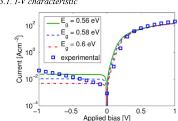
3.1. I-V characteristic
Fig. 1. Experimental and simulated (for three different GeSn layer band gaps) I-V curves of the pGeSn/nGe
heterostructure.
The experimental I-V curve in Figure 1 shows a ratio of 104 between the current at +1V and -1V bias. The
ideality factor of the diode is comprised between 1.25 and 1.3, indicating a possible SRH recombination component in forward operation. After an approximate bias of 0.25V, the current is, however, limited by the series resistance. Both the ideality factor and the current ratio make these diodes good candidates for use in GeSn MOSFETs[6]. Simulations of a structure similar to the experimental one show the same forward behavior as the experimental data. In reverse bias, the simulation is seen to differ from the experimental measurements, with the reverse current being constant. The simulations show, though, that the reverse saturation current is strongly dependent on the band gap of the GeSn layer, as is expected by the theory[7]. The influence of the carrier mobilities and the possible presence of defects in the GeSn layers have also been investigated but seem to have an effect that is at least one order of magnitude lower than that of the band gap energy on the value of the reverse saturation current. Work is still ongoing to clarify the precise origin of the experimental behavior in reverse bias, such as the addition of different distributions and types of defects to our model.
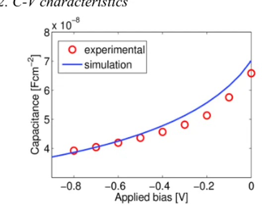
3.2. C-V characteristics
Fig. 2. Experimental and simulated C-V curves of the pGeSn/nGe heterostructure.
C-V measurements have also been performed and show a typical behavior in reverse bias, as can be seen in Figure 2. 1/C2 analysis shows a very linear
evolution and the corresponding carrier concentration has been calculated for several devices and contact area, with values ranging from 1.4 x 1016 cm-3 to 2 x
1016 cm-3, depending on the contact diameter, as
indicated in Fig. 3. This carrier concentration is linked to that of the Ge substrate, as its carrier concentration is expected to be much lower than that of the GeSn layer.
Fig. 3. Calculated carrier concentrations for various diode diameters.
Simulations of structures with similar material parameters show C-V characteristics that are in agreement with the experimental measurements, as can be seen in Figure 2. Features of the C-V characteristics indicating a possible link between the maximum of the capacitance for small forward biases and the value of the GeSn layer doping concentration still have to be confirmed experimentally.
Figure 4 shows the simulated microscopic carrier concentration of both holes and electrons as a function of position within the structure and for two different biases. The depletion region, located around the interface (x=0) is seen to extend mostly into the Ge substrate (positive x values), as expected from the much lower doping of the Ge substrate. When a
reverse bias of -0.2 V is applied, the depletion region widens, as expected. The value of the simulated capacitance is also directly linked to the width of this depletion region, which confirms the earlier 1/C2
analysis to calculate the doping concentration.
Fig. 4. Simulated microscopic carrier concentration as a function of position (x=0 is the interface).
3. Conclusions
I-V characteristics of pGeSn/nGe diodes have been measured and show very interesting properties. Simulations of the same structure are able to reproduce most of the observed behavior and point to the predominant influence of parameters such as the band gap energy of the GeSn layer. C-V characteristics showing little frequency dependence have also been measured, and their analysis for the determination of the carrier concentration is confirmed by simulations. More investigations of the effect of temperature, of other observed features in the C-V characteristics and of other defects at the interface or in the bulk of either layers, are still required in order to explain some of the observed behaviors, notably the reverse saturation current.
References
[1] B. Vincent, Y. Shimura, S. Takeuchi, T. Nishimura, G.Eneman, A. Firrincieli, J. Demeulemeester, A. Vantomme, T. Clarysse, O. Nakatsuka, et al., Microelectronic Engineering, 88, 342 (2011)
[2] G. Han, S. Su, Q. Zhou, P. Guo, Y. Yang, C. Zhan, L. Wang, W. Wang, Q. Wang, C. Xue, B. Cheng and Y-C. Yeo, IEEE electron device letters, 33(5), 634 (2012) [3] B. Vincent, F. Gencarelli, H. Bender, C. Merckling, B.
Douhard, D. H. Petersen, O. Hansen, H. H. Henrichsen J. Meersschaut, W. Vandervorst, M. Heyns, R. Loo, and M. Caymax. Appl. Phys. Lett. 99 , 152103 (2011)
[4] F. Gencarelli, B. Vincent, L. Souriau, O. Richard, W. Vandervorst, R. Loo, M. Heyns, Thin Solid Films, 520(8), 3211 (2012)
[5] B. Baert, O. Nakatsuka, S. Zaima, N.D. Nguyen, ECS Transactions, 50(9), 481 (2013)
[6] G. Han, S. Su, L. Wang, W. Wang, X. Gong, Y. Yang, …, Y. C. Yeo, In VLSI Technology, 2012 Symposium on, 97 (2012)
[7] S. M. Sze, K. K. NG, Physics of Semiconductor Devices, Wiley, 2006