UNIVERSITÉ DE MONTRÉAL
ISOTOPE ENGINEERING AND LATTICE DISORDER IN GROUP IV NANOSCALE AND QUANTUM SEMICONDUCTORS
SAMIK MUKHERJEE
DÉPARTEMENT DE GÉNIE PHYSIQUE ÉCOLE POLYTECHNIQUE DE MONTRÉAL
THÈSE PRÉSENTÉE EN VUE DE L’OBTENTION DU DIPLÔME DE PHILOSOPHIAE DOCTOR
(GÉNIE PHYSIQUE) JUILLET 2017
ÉCOLE POLYTECHNIQUE DE MONTRÉAL
Cette thèse intitulée:
ISOTOPE ENGINEERING AND LATTICE DISORDER IN GROUP IV NANOSCALE AND QUANTUM SEMICONDUCTORS
présentée par : MUKHERJEE Samik
en vue de l’obtention du diplôme de : Philosophiae Doctor a été dûment acceptée par le jury d’examen constitué de :
M. MÉNARD David, Ph. D., président
M. MOUTANABBIR Oussama, Ph. D., membre et directeur de recherche M. ROCHEFORT Alain, Doctorat., membre
DEDICATION
আমার বাবা, মা, জ্যেঠু, ও স্বর্গীয় দাদু ঠাকুমা জ্ক
To my father, my mother,
my uncle, and
ACKNOWLEDGEMENTS
I am grateful for all the support and guidance I have received over the last four and half years at Polytechnique Montreal. First and foremost, I am immensely grateful to my advisor Prof. Oussama Moutanabbir, for giving me the opportunity to work in his research group. It has been an honor to share the title along with Dany, of being his first Ph.D. student at Polytechnique Montreal. I appreciate all his wonderful insights, the contributions of time, ideas, laboratory freedom, and the fundings to make my Ph.D. experience a productive and joyous one. The enthusiasm and passion he has for research are very contagious and have motivated me through the difficult patches in pursuit of my Ph.D..
I am also grateful to my Ph.D. committee members: Prof. Chennupati Jagadish, Prof. David Ménard, and Prof. Alain Rochefort for their precious time and interest in evaluating my thesis and providing me with valuable suggestions. I will forever be thankful to my former research advisors Prof. Nikhil Ranjan Das and Prof. Elizabeth Boer-Duchemin. They were immensely helpful in providing advice many times during my graduate school career.
I thank all our collaborators for their help and assistance on several research projects: Prof. K. Itoh and Dr. T. Sekiguchi (Keio University, Japan), Dr. M. de la Mata and Prof. J. Arbiol (ICN2 and ICMAB, Barcelona, Spain), Dr. U. Givan and Dr. S. Senz (Max Planck Institute, Halle, Germany), Prof. S. Francoeur, N. Kodali, and A. Bergeron (Polytechnique Montreal), Dr. H. Watanabe (AIST, Ibaraki, Japan), Dr. S. Wirths and Dr. D. Buca (Peter Grünberg Institute, Juelich, Germany), and Dr. J. Hartmann (CEA-LETI, Minatec, Grenoble, France). I am especially grateful to the Northwestern University Center for Atom Probe Tomography (NUCAPT) for hosting me for the atom probe experiments and to Dr. D. Isheim and Prof. D. Seidman for the time spent together at their lab at Northwestern University and for sharing with me their vast knowledge and experience on atom probe tomography.
I gratefully acknowledge the various funding agencies like the Natural Sciences and Engineering Research Council of Canada (NSERC), Fondation de l’Ecole Polytechnique de Montréal, Canada Research Chair, Canada Foundation For Innovation, MRIF-Québec, Regroupement Québécois Matériaux de Pointe(RQMP), and Max Planck Society for funding this research.
My special gratitude goes to Joël Bouchard, Christophe Clément, Marie-Helene Bernier, and Samir Eloutik for their technical assistance. I also thank the wonderful staff in the Department of Engineering Physics for always being so helpful and friendly. People here are genuinely nice and want to help out. Special thanks go out to Adèle, Lyne, and Joanne.
Throughout all the time I spent at Polytechnique Montreal, my friends and colleagues became a part of my life. My heartiest thanks go to all of them: Dany, Anis, Simone, Olga, Marc, Zeinab, Matthieu, Jerome, Julien, Etienne, Aashis and all the past members of the Moutanabbir group. It was a pleasure to work, do sports, and spend time with them. Best wishes to Dany as he finishes up. Special thanks to Simone, Olga, and Anis for all the camping, hiking trips, the peak-productivity Wednesdays, and the numerous other memories which I can never forget. I also thank my friends Prajwal, Suchakra, Tanushree, Alice, Francis, Anna, Emma, Daniel, Leigh, Dennis, Roksana, Sara, Emily, Debashis, Deboshree, Kaustav (apologies if I have missed someone!) for the support and friendship that I needed.
My special thanks go out to my cousins and friends back in India: Sayak, Butai, Joy, Partho, Gopal, Debjit, Riu, Raja, Pritha, Keya, Anik, Syam, Biswarup, Debayan, Saion, Abhinaba, Pushpargha, Sandeep, Sumanta, Alak, Pratik, Mrinmoy, Soham, Sandip (too many in the list but you know who you are!) for keeping me smiling, happy and relaxed and for making my every trip back home really memorable. I extend my gratitude to my former teachers at my school and college who had the biggest influence on me: Mr. K.P. Mukherjee, Fr. J. Pathickal, Fr. T.S. Gomes, Prof. A. Dasgupta, Prof. D. Sengupta, Prof. A. Lahiri, Prof. A.C. Gomes, Prof. B. Bandhopadhay, Prof. P.C Rakshit, Prof. A.D. Burman. They not only remain my role model as ideal teachers and mentors but are also the reason I took up research as a career.
Finally, through all this I received unyielding love, support and encouragement of my entire family. I am out of words to express my gratitude to my uncle Bholanath Mukherjee, who has been like a father-figure to me since my childhood days. I dearly miss my late grandparents Rohininandan and Jaminibala Mukherjee, but their blessings are always with me. I wished they lived a few more years to see me graduate. I especially thank my mom and dad. My hard-working parents have sacrificed their lives for me and provided unconditional love and care. I love them so much, and I would not have made it this far without them.
RÉSUMÉ
L’ingénierie des isotopes stables est la manipulation artificielle de la composition et de la distribution des isotopes stables d’un élément dans la maille cristalline d’un matériau donné. Au cours des deux dernières décennies, de nombreuses études conduites sur des semi-conducteurs monocristallins ont montré que de telles modifications peuvent altérer considérablement leurs propriétés fondamentales comme les propriétés nucléaires, le comportement des phonons, le diagramme des bandes d’énergie et le paramètre de maille. Ces développements ont permis un nouvel élan d’innovation et d’applications potentielles exploitant l’ingénierie isotopique dans le transport thermique et thermoélectrique, dans l’optoélectronique, et dans le traitement quantique de l’information, parmi tant d’autres.
L’essentiel de la littérature relative à l’ingénierie des isotopes à l’échelle quantique ou nanoscopique se concentre principalement sur des investigations théoriques. A ce jour, les études expérimentales demeurent absentes malgré leur importance dans l’élucidation d’un vaste éventail de phénomènes quantiques et nanoscopiques. Dans cette thèse, nous explorons ce paradigme méconnu en concentrant nos expérimentations sur les propriétés de base des structures dont la composition isotopique est contrôlée à l’échelle nanoscopique. Des nanofils isotopiquement pures de 29Si ou d’alliage isotopique 28Si
x30Si1-x ont été synthétisés à l’aide de la méthode vapeur-liquide-solide et leurs propriétés de transport des phonons ont été étudiées en utilisant la nanothermométrie Raman. La composition et la distribution isotopiques des nanofils individuels ont été déterminées à l’aide de la sonde atomique tomographique assistée par laser. Cependant, avant que la sonde atomique tomographique ne soit appliquée pour imager les isotopes dans un nanofil, l’utilisation de cette technique unique, mais néanmoins extrêmement délicate, a été d’abord optimisée grâce à deux systèmes additionnels. Le premier système de matériaux consiste en un super réseau isotopique de diamant, et le deuxième est une série d’alliages ternaires métastables de silicium-germanium-étain. Ces recherches nous ont permis non seulement de développer nos connaissances et notre maîtrise de la sonde atomique tomographique, mais également de faire des nouvelles découvertes intéressantes.
En exploitant l’imagerie tridimensionnelle atomique d’alliages ternaires métastables, nous avons obtenu des preuves solides que ces alliages sont parfaitement monocristallins et croissent sans agrégats d’étain même pour des concentrations supérieures à la composition attendue de
l’équilibre thermodynamique. Cependant, en augmentant la quantité d’étain, nous avons montré que la distribution du silicium dans ces alliages s’éloigne de la distribution théorique idéale. La principale cause de cet ordre atomique à courte portée est la présence d’une interaction répulsive entre les atomes de silicium et les atomes d’étain. L’étude menée sur le super réseau isotopique de diamant à l’aide de la sonde atomique tomographique a montré pour la première fois qu’il est en effet possible de contrôler le phénomène d’évaporation par effet de champ, un seul atome à la fois, d’un matériau comme le diamant, possédant le plus haut champ d’évaporation connu. Afin d’expliquer la physique sous-jacente de ce résultat, nous proposons un mécanisme détaillé de l’évaporation par effet de champ assistée par laser de nanofils de diamant.
Toute l’expertise acquise de ces mesures tomographiques fut mobilisée pour l’analyse des nanofils d’alliage isotopique 28Six30Si1-x. Les expériences ont révélé que les deux isotopes du silicium sont distribués de manière non uniforme dans un nanofil 28Six30Si1-x, avec l’isotope 28Si plus léger proche de la surface et l’isotope 30Si plus lourd au cœur du nanofil. Ces observations révèlent des nouveaux détails sur le comportement des atomes de silicium à l’interface liquide-solide pendant la croissance vapeur-liquide-liquide-solide via un catalyseur métallique. En fait, nous observons que la cristallisation des nanofils met en jeu des mécanismes qui paraissent sensibles à la masse atomique, amenant ainsi de nouvelles connaissances fondamentales sur la dynamique de croissance épitaxiale à l'échelle nanométrique. Les mesures de nanothermométrie Raman sur ces nanofils à la composition isotopique contrôlée ont révélé que la conductivité thermique des nanofils isotopiquement désordonnés 28Si
x30Si1-x est réduite de ~25 − 30% au voisinage de la température ambiante par rapport à celle des nanofils isotopiquement purs en 29Si. Le comportement des phonons a été également étudié dans une série supplémentaire d’alliages isotopiques 28Si
x30Si1-x avec des inclusions polytypiques de segments lamellaires hexagonaux selon l’axe longitudinal des nanofils. Nous avons montré que ces segments hexagonaux à l’intérieur des nanofils voient leur température augmenter plus rapidement en comparaison aux segments de maille cubique de type diamant dans le même nanofils. Nous avons aussi observé que la conductivité thermique globale de ces nanofils d’alliage isotopique avec polytypes est réduite de ~10% par rapport à son équivalent à maille cubique de type diamant, proche de la température ambiante.
Au cœur de cette thèse se trouve la première démonstration expérimentale de la synthèse, de la caractérisation et de l’étude des effets du désordre cristallin dans des nanofils de silicium à la composition isotopique contrôlée. L’impact de ce travail réside dans la rigoureuse démonstration
expérimentale de la manipulation de la composition isotopique et de la distribution des éléments lors de la croissance de nanostructures ainsi que dans la caractérisation précise des effets des isotopes sur leurs propriétés fondamentales. Par conséquent, ce travail prépare le terrain pour le développement d’une famille complètement nouvelle de structures nanoscopiques et quantiques à la composition isotopique contrôlée visant des applications dans le transport de chaleur à l’échelle nanoscopique, les dispositifs thermiques quantiques, et le traitement quantique de l’information, pour en nommer quelques-uns. Cette thèse soulève également de nouvelles questions fondamentales ainsi présentant des opportunités pour des études futures.
ABSTRACT
Stable isotope engineering refers to the artificial manipulation of the content and distribution of the stable isotopes of an element within the lattice of a material. Over the last two decades, numerous studies conducted on bulk semiconductors have shown that exercising such a control can significantly alter the fundamental behavior of a material such as the nuclear properties, phonon behavior, electronic energy gaps, and lattice constant. Consequently, a myriad of opportunities emerged from this isotopic engineering of semiconductors enabling a variety of novel and potential applications such as thermal transport and thermoelectric, optoelectronics, and quantum information processing, to name a few.
The body of literature related to isotope engineering in nanoscale materials is made primarily of theoretical investigations. Till date, the experimental investigations remain conspicuously missing, despite the fact that the combination of mass-related effects and size-related effects can provide a rich playground to uncover and harness a wide range of new nanoscale and quantum phenomena. In this thesis, we unfold this unexplored paradigm by focusing our experimental investigations on the basic lattice properties of isotopically programmed nanoscale structures. The isotopically pure 29Si and mixed Si28 x30Si1−x nanowires were synthesized using the metal catalysed vapor-liquid-solid method and the phonon transport in these nanowires was studied using Raman nanothermometry. The isotopic composition and distribution within an individual nanowire was investigated using laser-assisted atom probe tomography. However, before the atom probe tomography could be implemented to map the isotopes within a nanowire, the experimental capabilities of this unique yet extremely challenging technique were first optimized in two additional systems. The first material system consists of diamond isotopic superlattice and the second, a set of ternary metastable silicon-germanium-tin alloys. These investigations not only equipped us with the science and the practice of atom probe tomography, but also had some interesting revelations of their own.
Based on the atom-by-atom three-dimensional mapping of ternary metastable alloys, we obtained clear evidence that these alloys grew without any tin clustering even at contents larger than the equilibrium composition. However, with the increase in tin content, the silicon distribution within these alloys was found to deviate from the ideal theoretical distribution. The root cause of this short-range atomic ordering is the presence of a repulsive interaction between silicon and tin
atoms. The atom probe investigations of the isotopic diamond superlattice showed for the first time that it is indeed possible to control the process of field evaporation in an atom-by-atom fashion from a material like diamond with the highest known evaporation field. To explain the underlying physics of this achievement, we proposed a detailed mechanism of the laser-assisted field evaporation of diamond nanotips.
All the expertise gained from these atom probe measurements were summoned in for analysing a single isotopically mixed 28Six Si
1−x
30 nanowire. The investigations revealed that the two silicon isotopes are non-uniformly distributed within a 28Six30Si1−x nanowire with the lighter
Si
28 isotope rich near the surface and the heavier 30Si isotope rich at the core of a nanowire. This revelation sheds a new light on the atomistic-level behavior of silicon atoms at the liquid-solid interface during the metal catalyzed vapor-liquid-solid growth. In fact, we observed that the nanowire crystallization involves processes that are seemingly mass-sensitive thus providing new fundamental insights on the dynamics of the nanowire growth. The Raman nanothermometric measurements on these isotopically engineered nanowires revealed that the lattice thermal conductivity of the isotopically mixed 28Six30Si1−x nanowires is reduced by a ~25 − 30% relative to the isotopically pure 29Si nanowires around the room temperature. The phonon behavior was also studied on a different set of isotopically mixed 28Six Si
1−x
30 nanowires with polytypic inclusions of lamellar hexagonal segments along their long axis. The hexagonal segments in these nanowires were found to heat up more rapidly compared to the diamond cubic segments and the overall lattice thermal conductivity of these polytypic isotopically mixed nanowires to be reduced by ~10% relative to its diamond cubic counterpart, close to room temperature.
At the core of this thesis is the first experimental demonstration of the synthesis, characterization, and the investigations of the lattice disorder effect in isotopically engineered silicon nanowires. Its impact lies in providing clear experimental demonstration of the manipulation of the isotopic content and distribution during the growth of nanostructures and a precise characterization of the effects of isotopes on their fundamental properties. Hence, this thesis lays the groundwork for the development of an entirely new family of isotopically engineered nano and quantum structures relevant for applications in nanoscale heat transport, quantum thermal devices, and quantum information processing, to name a few. The thesis also raises some new fundamental questions creating a wealth of opportunities for future studies.
TABLE OF CONTENTS
DEDICATION………iii ACKNOWLEDGEMENTS………..…..iv RÉSUME………...…..vi ABSTRACT………....…ix TABLE OF CONTENTS………..…….….xi LIST OF TABLES……….……xiv LIST OF FIGURES………...…....….xv LIST OF ABBREVIATIONS……….…..xxv LIST OF SYMBOLS………...…...…..xxvii LIST OF APPENDICES………...…..xxxii CHAPTER 1 INTRODUCTION………..…..…………..1 1.1 Overview ... 1 1.2 Motivation ... 31.3 Objectives and Methodology ... 6
1.4 Thesis Organization ... 7
CHAPTER 2 LITERATURE REVIEW………9
2.1 Stable Isotope Engineering in Group IV Semiconductors ... 9
2.1.1 Isotope Separation ... 9
2.1.2 Stable Isotope Effect on Fundamental Properties of Semiconductors ... 11
2.1.3 Impact of Isotope Engineering on Semiconductor Physics ... 18
2.2 Atom Probe Tomography on Nanoscale Materials ... 28
2.2.1 Roadmap to Modern Day Atom Probes ... 28
2.2.3 3D Tomographic Imaging ... 32
CHAPTER 3: EXPERIMENTAL TECHNIQUES: INSTRUMENTATION AND UNDERLYING MECHANISMS………...………...37
3.1 Atom Probe Tomography ... 37
3.1.1 Instrumentation ... 37
3.1.2 The Physics of Field Evaporation ... 44
3.2 Raman Scattering Spectroscopy ... 49
3.2.1 Instrumentation ... 49
3.2.2 Inelastic Scattering of Light ... 51
3.3 Transmission Electron Microscopy ... 56
CHAPTER 4: ARTICLE 1: LASER-ASSISTED FIELD EVAPORATION AND THREE- DIMENSIONAL ATOM-BY-ATOM MAPPING OF DIAMOND ISOTOPIC HOMOJUNCTIONS….……..………62
4.1 Authors ... 62
4.2 Abstract ... 62
4.3 Introduction ... 63
4.4 Experiment... 64
4.5 Results and Discussion ... 67
4.6 Summary... 82
4.7 Acknowledgement ... 83
CHAPTER 5: ARTICLE 2: SHORT-RANGE ATOMIC ORDER IN NON- EQUILIBRIUM SILICON-GERMANIUM-TIN SEMICONDUCTORS………..……...84
5.1 Authors ... 84
5.2 Abstract ... 84
5.4 Experiment... 86
5.5 Results and Discussion ... 87
5.6 Summary... 94
5.7 Acknowledgement ... 94
CHAPTER 6: ARTICLE 3: PHONON ENGINEERING IN ISOTOPICALLY DISORDERED SILICON NANOWIRES………..95
6.1 Authors ... 95
6.2 Abstract ... 95
6.3 Introduction ... 96
6.4 Experiments ... 97
6.5 Results and Discussion ... 100
6.6 Summary... 113
6.7 Acknowledgement ... 114
CHAPTER 7: ROLE OF ISOTOPE DISORDER AND DEFECT IN HEAT TRANSPORT IN SILICON NANOWIRES………115
7.1 Elucidating the Isotope Distribution within a 28Si x30Si1-x NWs ... 115
7.2 Raman Spectroscopy on Suspended Nanowires ... 122
7.2.1 Isotopically Pure and Isotopically Mixed Nanowires ... 122
7.2.2 Isotopically Mixed Nanowires with Stacking Faults ... 125
CHAPTER 8: GENERAL DISCUSSION………135
CHAPTER 9: CONCLUSION AND RECOMMENDATIONS…….……….139
BIBLIOGRAPHY………...……….144
LIST OF TABLES
Table 1.1 Stable isotopes of C, Si, and Ge, along with their natural abundances, atomic mass, nuclear spin, and neutron capture cross-section……….………...2
LIST OF FIGURES
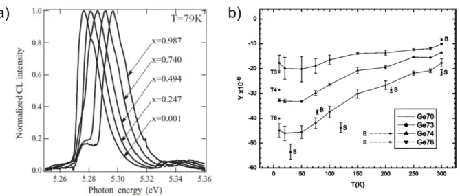
Figure 2.1: (a) The evolution of the phonon energies (Raman frequencies) of different isotopically engineered Si samples with 〈m〉. (Reproduced with permission from Widulle et al. [30]). (b) The evolution of the Raman line width of the different isotopically engineered Ge samples with 〈m〉. (Reproduced with permission from Zhang et al. [33]). ... 12 Figure 2.2: (a) Free excitonic CL spectra collected at T = 79 K from different isotopically
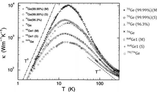
engineered C diamond films. (Reproduced with permission from Watanabe et al. [49]). (b) x-ray back scattering measurement results on the fractional change in relaxed lattice constant ∆a/a of 73Ge, 74Ge, and 76Ge with respect to 70Ge as a function of temperature. The abscissa represents Y = (a〈m〉− a70)/a70 in ppm. The points labelled T3, T4, and T6 are theoretical calculated values of Y at T = 0K, for 73Ge, 74Ge, and 76Ge respectively. (Reproduced with permission from Hu et al. [5]). ... 16 Figure 2.3: Evolution of the lattice thermal conductivity of different isotopically engineered Ge
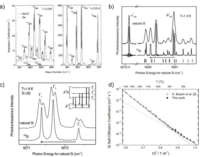
samples: 70Ge(99.99%), 70Ge(96.3%), 76Ge(86.3%), NatGe, and 70/76Ge as a function of temperature. The 70/76Ge sample had 43.0% of 70Ge and 48.0% of 76Ge and residual 72Ge and 74Ge. M and S represents the measurements done at labs in Moscow and Stuttgart respectively. The black dotted lines represent the T3 and T−1 dependence of κ at low and high temperatures respectively. (Reproduced with permission from Asen-Palmer et al. [55]). For clarity, the figure legends are highlighted alongside. ... 19 Figure 2.4: (a) LVS of NatGe2:16O (left) and the superimposed spectra of enriched jGe2:16O j = 70, 73, 74, 76 (right). (Reproduced with permission from Mayur et al. [69]). (b) High resolution NP PL lines of excitons bound to neutral B (BNP1 ) and P (αNP1 ) impurities in NatSi (top) and enriched 28Si(bottom). (c) High-resolution NP lines of excitons bound to neutral Al acceptor in NatSi (top) and enriched 28Si (bottom). Inset: Energy level diagram showing the doublet splitting of the A0 ground state in NatSi (absent in enriched 28Si) as well as the triplet A0X excited state. The spectrum in both (b) and (c) obtained from 28Si is red-shifted by 0.92 cm−1 (the length of the arrow) to account for the band gap difference between the two. (Both (b) and (c) reproduced with permission from Karaiskaj et al. [72]). (d) Evolution of DSD for Si as a function of annealing temperature. The solid circles represent the DSD values obtain from Raman spectroscopic investigation [73], while the open circles represent the DSD values
obtained from the SIMS measurements. The dashed and the dotted lines represent the contribution of self-interstitial and self-vacancy to DSD. (Reproduced with permission from Bracht et al. [74]). ... 23 Figure 2.5: (a) Schematics of a proposed five 29Si QIP device with a field gradient applied in the
direction of the qubit chain for qubit selectivity. The 31P at the end of the chain is for qubit readout. (Reproduced with permission from Itoh et al. [85]). (b) SEM image of a QIP device showing the location of the 31P electron spin and NS qubit in a top gated nanostructure on a NS-free 28Si platform. (Reproduced with permission from Muhonen et al. [90]). ... 27 Figure 2.6: (a) From the top: A LiMnO2 nanoparticle, electrostatically attached to a micro-needle
is being transferred to a micro-post. The micro-needle detached from the nanoparticle. A protective Pt layer deposited over the nanoparticle. Needle shaped tip prepared by annular ion-milling. (Reproduced with permission from Devraj et al. [106]). (b) Top: A single NW, picked up using a W micro-needle and is being placed into a FIB-bored hole on the top of the APT micro-tip post. Bottom: The micro-needle detached from the NW. (Reproduced with permission from Sanford et al. [107]). (c) Top: APT micro-posts on Si (111) produced by dicing the wafer and subsequent etching of the particulates left by the grinding. Bottom: Si NWs directly grown on a micro-post. The scale bar in the top and the bottom figures represent 5 μm and 100 nm respectively. (Reproduced with permission from Perea et al. [108]). (d) Top: A W micro-needle is being used to pick up a NW from a TEM grid. Bottom: The NW welded to the micro-needle inside a Dual-FIB. (Reproduced with permission from Agarwal et al. [109]). (e) From left: A W micro-needle (green) is being used to pick up a dummy NW (blue). The dummy NW is being used to pick up the target NW (red). The target NW is being welded to an APT micro-post (yellow). The dummy NW is detached from the target NW without dislodging the latter from its position. (Reproduced with permission from Koelling et al. [110]). (f) From left: The short Si NWs coated with Ni/Pt in FIB. Circular markers are laid, each centered on a single NW and a thin lamella, containing 3 NWs, is milled out. The lamella is lifted out using a micro-needle and welded to an APT micro-post with the marker right at the center of the post. FIB milling the structure into the desired shape of an APT tip with the NW in its center. (Reproduced with permission from Blumtritt et al. [111]). ... 31
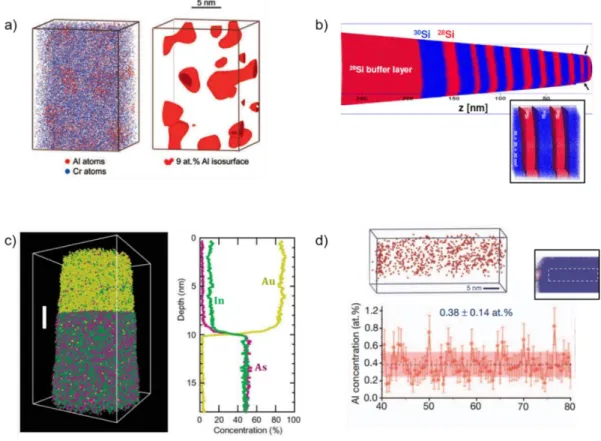
Figure 2.7: (a) 3D distribution showing the Al and Cr atoms within a Ni-Al-Cr alloy (left) and the location of a fraction (30%) of the γ′ precipitate, denoted by 9.0 at.% Al iso-concentration surfaces (right). (Reproduced with permission from Yoon et al. [117]). (b) 3D atom-by-atom mapping of the 28Si and 30Si isotopes within a 28Si/30Si superlattice. (Reproduced with permission from Moutanabbir et al. [118]). Inset: The homointerfaces drawn at 50.0 at.% of 28Si isoconcentration surface. (c) 3D distribution of atoms within a InAs NW. Alongside, the proximity histogram, depicts the 1D concentration profile of the In (green), As (purple), and Au (yellow) atoms across the catalyst-NW interface. (Reproduced with permission from Perea et al. [131]). (d) The 3D distribution of Al impurity atoms along the growth axis of a Si NW (top). The axial concentration of Al atoms along the growth axis of a Si NW (bottom). The concentration was averaged over a cylinder of diameter 10nm (inset). The black dotted line depicts the average axial concentration within the cylinder and the shaded region depicts the uncertainty of the measured average concentration (which is about 0.14 at.%). (Reproduced with permission from Moutanabbir et al. [138]). ... 36 Figure 3.1: (a) Schematic illustration of an APT setup showing the needle shaped tip, the local
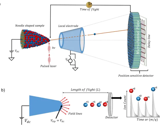
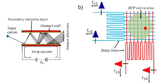
electrode, the position sensitive detector (MCP and the delay line) and a pulsed laser being applied to the tip. (b) Schematic illustration of a time-of-flight mass spectrometer. ... 38 Figure 3.2: (a)-(b) Schematic illustration of the two key components of an APT detector: (a) a
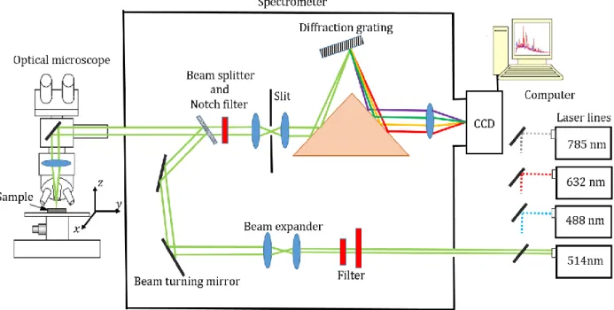
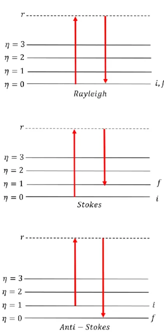
microchannel plate, and (b) a delay line detector. ... 43 Figure 3.3: Schematic illustration, showing the different components of a Raman spectrometer. 50 Figure 3.4: Energy level diagram related to the Rayleigh, Raman Stokes, and Raman Anti-Stokes
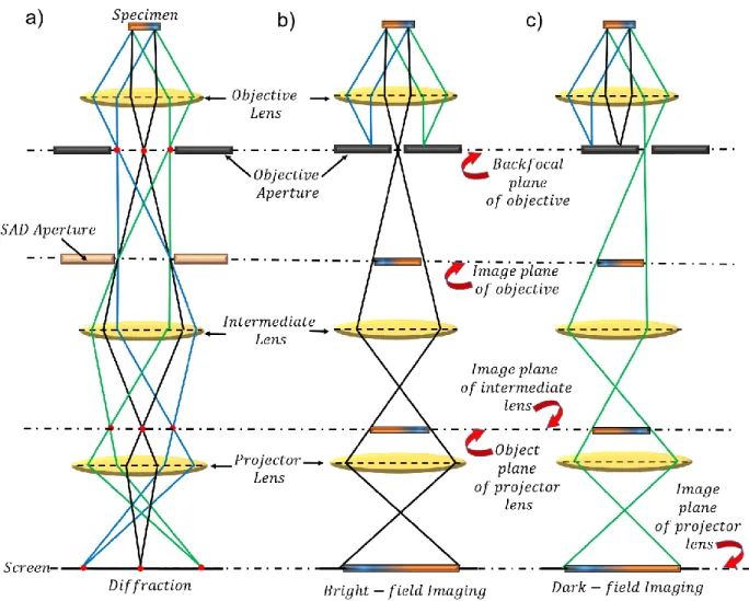
scattering of light. ... 54 Figure 3.5: Ray diagram depicting the position of each lens and aperture, located between the
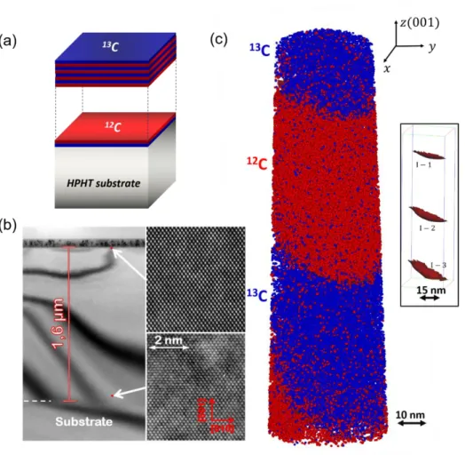
specimen and the screen in a TEM column during operations in (a) the diffraction mode (b) the bright field imaging mode and (c) the dark field imaging mode. ... 59 Figure 4.1: (a) Schematics of the CVD-grown isotopically modulated 12C/13C nanoscale layers
investigated in this work. (b) Cross-sectional transmission electron microscopy image of the as-grown diamond superlattice. Insets: High-resolution TEM images of regions near the surface (top) and interface with HPHT substrate (bottom) demonstrating the high crystalline
quality of the sample. The growth direction of sample is (001). The scale bar is the same for the top and bottom image. c) 3-D atom-by-atom reconstruction of the isotopically modulated diamond superlattice sample. The analysis direction of the sample is also (001). The 12Catoms are shown in red bubbles and the 13C atoms are shown in blue bubbles. For the sake of clarity, only 10% of the collected atoms are displayed. Inset: The interface between 12C and 13C, defined as isoconcentration surfaces drawn at 50 at.% concentration of 12C. ... 65 Figure 4.2: Sequential steps of FIB fabrication APT nanotips. (a) A small piece of the as grown
sample was first coated with Ni (70 nm) and then Pt (0.15 µm). Trenches were milled on 3 sides of a chosen section on the sample by Ga+ ion (30 kV) FIB milling. (b) After milling off the 4th side, the section was lifted out using a micromanipulator. (c) The section was then attached to an APT micro-post using cold Pt welding. (d) To initiate the nanotip sharpening process, first a pyramidal shape was given to the attached sample using rectangular milling patterns. (e), (f), and (g) Circular milling patterns of varying diameter were used to give the sample a needle like shape to the nanotip. (h) Final polishing of the nanotip was done using low energy Ga+ ions (5 kV) (i) Final shape of the APT nanotip before inserting into the APT chamber. ... 66 Figure 4.3: (a) Mass spectra recorded at Epulse=1000 pJ, showing singly, doubly, and triply
charged states of both 12C and 13C (in blue). The spectra reveal clusters with a maximum size up to 3 carbon atoms. The inset showing the mass spectra up to m/n = 120 Da confirming the absence of clusters higher than three carbon atoms. We also see some additional weak peaks in the mass spectra that are not labelled. For example, the peaks at 22 Da and 22.5 Da can be attributed to CO12 22+ and CO
2 2+
13 respectively. The peaks at 28 Da and 30 Da most likely originate from N2+ and NO+. (b) The proximity histogram showing the atomic concentration of both12C (in red) and 13C (in blue) along the long axis of the tip (z axis in Figure 1(c)). (c) The comparison between the normalized mass spectra of 13C2+ recorded at E
pulseof 500pJ (blue spheres) and 1000pJ (red spheres). The width of the mass spectra was calculated by fitting the raw data with Lorentzian line shapes (continuous black lines). There is an additional (cannot be identified at the moment) peak present (marked by black arrows) just before the 13C2+ peak. This was not taken into account during the fitting (d) The comparison between the normalized mass spectra at Epulse =1000pJ for of 13C2+ atoms located at the surface on the
dark side (red spheres) and the illuminated side (blue spheres) of the nanotip. The width of the mass spectra was calculated by fitting the raw data with Lorentzian line shapes (continuous black lines). Note that the unidentified additional peak disappears in the mass spectra for the surface atoms. ... 69 Figure 4.4: (a) Schematics depicting various diffusion processes (details in text). (b) Normalized
concentration profile for 13C atoms at the surface (dark side) of the nanotip at I-1 for Epulse= 1000 pJ and 500 pJ. The data points are displayed with sphere (green and blue spheres for 1000pJ and 500pJ respectively). In (b), (c), and (d) the red dashed lines are the cubic spline interpolation of the raw data and continuous black line is the fit using Fick’s second law. (c) Normalized concentration profile for 13C atoms at the surface (dark side) of the nanotip at I-1 and I-2 for Epulse = 1000 pJ. The data points are displayed with sphere (blue and green spheres for I-1 and I-2 respectively). Inset: Displaying only the Fick’s law fitting of the raw data. It is clear, that the diffusion length of the 13C atoms at the surface (dark side) of the nanotip is more at I-2 than at I-1. (d) Normalized concentration profile for 13C atoms at the core of the nanotip at I-1 and I-2 for Epulse = 1000 pJ. The data points are displayed with sphere (blue and green spheres for I-1 and I-2 respectively). Inset: Displaying only the Fick’s law fitting of the raw data. It is evident that the diffusion length of the 13C atoms at the core of the nanotip is more at I-2 than at I-1. Also, the diffusion length of the 13C atoms at the core of the nanotip at I-1 or I-2 is much less that that at the surface for the same pulse energy ... 76 Figure 4.5 : (a) Plot of normalized concentration of +q, +2q and +3q (inset) cations with radial
distance for EPulse = 1000 pJ. The +2q and +3q (inset) cations have the highest concentration roughly at the center which corresponds to the center of the nanotip (reason explained in the text). (b) Plot of normalized concentration of mono, di, and tri atomic species with radial distance for EPulse = 1000 pJ. The minima in the concentrations of di and tri atomic specis occur roughly at the center of the nanotip(reason explained in the text). Also noteworthy is that the location of the extremum values occurs slightly to the right in both the figures rather than being exactly at the center. This might be due to the fact that the nanotip had an inherent asymmetry from the FIB fabrication process or the non-uniform temperature distribution has shifted the field extrema from the center to one side of the nanotip. ... 80
Figure 5.1: (a) High angle annular dark field STEM (top) and high resolution STEM (bottom) images of the Si0.04Ge0.84Sn0.12/Ge interface. Inset: A diffraction pattern taken from a selected region at the interface (b) 3-D reconstruction of the ternary alloy (Si0.04Ge0.84Sn0.12), showing the Ni capping layer, the SiGeSn thin film and a portion of the Ge buffer layer. For the sake of clarity, only 10% of Ge atoms and 50% of Sn atoms are displayed. ... 86 Figure 5.2: (a) Frequency distribution of Si (green), Ge (blue), and Sn (red) in Si0.04Ge0.84Sn0.12 as
determined from APT reconstruction (in histograms). The corresponding binomial distribution of these atoms are shown in black continuous lines (b) The partial radial distribution function of Sn and Si atoms with respect to Sn (top), Ge (middle), and Si (bottom) in the same sample as in (a) for r = 10 nm. The Integrated Visualization and Analysis Software (IVAS) computed error bars are smaller than the data symbols. The black dotted line represents p − RDF =1. ... 88 Figure 5.3: (a) Frequency distribution of Si (green), Ge (blue), and Sn (red) in Si0.10Ge0.875Sn0.025 as determined from APT reconstruction (in histograms). The corresponding binomial distribution of these atoms are shown in black continuous lines. (b) The partial radial distribution function in the same sample as (a) for r = 10 nm of Sn atoms wrt. Sn (top), Si wrt. Si (middle), and Si wrt. Sn (bottom). The IVAS computed error bars are smaller than the data symbols. The black dotted line represents p − RDF =1. ... 91 Figure 5.4: (a) Si-Si and Sn-Sn NN 2, 3, and 5 distribution in the alloy containing 12.0 at.% Sn.
The distribution as determined from APT reconstruction are shown in solid spheres Si (green) and Sn (red). The corresponding binomial distribution are shown in black continuous lines. All the data sets are normalized with respect to the theoretical probability distribution, Pk(r, C). (b) Departure of the observed Si-Si and Sn-Sn NN 2, 3, and 5 distributions from the binomial distribution. The y-axis in all the three figures are the same. ... 92 Figure 6.1: (a) A schematic illustration of the VLS growth of the isotopically engineered Si NWs.
Vapor phase precursors are supplied to Au-Si eutectic droplet. For the isotopically pure NWs the precursor is 29SiH
4 (purity 99.9%) and for the isotopically mixed NWs, a mixture of 28SiH4 (purity 99.99%) and 30SiH
4 (purity 99.9%) was injected. Crystallization of Si atoms from the supersaturated droplet takes place at the droplet-nanowire interface which becomes the growth front. Inset: Low magnification SEM images of as grown isotopically mixed 28Six30Si1-x NWs
and isotopically pure 29SiNWs, both recorded at a tilt angle of 60º. The scale bars in both the figures denote 1μm. (b) STEM images of the isotopically pure 29Si NWs. Left: A single 29Si NW. The NW have grown along the [121] direction and the image taken from the [111] Si zone axis. The scale bar in the figure is 200nm. Middle: STEM image of the NW sidewalls showing gold decoration on the facets. The scale bar in the figure is 20nm. Right: High magnification STEM image (taken from the region marked by the red box in the middle image) and the power spectrum (fast Fourier transform (FFT)) in the inset shows the high crystalline quality of the NW. The scale bar in the figure corresponds to 1nm. (c) SEM image of a single 29Si NW after sonication and dispersion atop Au capped Si substrate. The scale bar denotes 1μm... 99 Figure 6.2: Si-Si LO normalized phonon spectra of 28Si
x30Si1-x NW and 29Si NW at different incident laser power densities. The spectra at 1.94 mw/µm2 and 0.08 mw/µm2 were recorded using the 488nm laser and the remaining spectra using the 532nm laser. The spectra shown here are representative of a single 28Si
x30Si1-x NW and a single 29Si NW. The data points for the 28Six30Si1-x NWs are shown as empty green squares and that of 29Si NWs correspond to empty red circles. The black continuous curve corresponds to the Voigt fit. ... 101 Figure 6.3: (a) and (b) represent measurements using 488nm laser at low incident power density
whereas (d) and (e) represent measurements using 532nm laser at high incident power density. In all figures, the empty blue squares correspond to the isotopically mixed 28Six30Si1-x NWs and the filled black circles represent the isotopically pure 29Si NWs. (a) and (d): Evolution of average peak position with incident laser power density for both 28Six30Si1-x NWs and 29Si NWs. (b) and (e): Evolution of the average FWHM with incident laser power density for both 28Si
x30Si1-x NWs and 29Si NWs. In (a) and (b) the averaging was done over measurements on more than 10 single NWs and in (d) and (e) the averaging was done over measurements on 7 single NWs. The error bars in (a), (b), (d), and (e) are double the standard deviation of the peak position and FWHM from respective average values. (c) and (f): Plots of the effective local temperature of the NWs extracted from the shift in average peak position in (a) and (d) respectively. The error bars represent the uncertainty in the calculated temperature due to the standard deviation of the measured peak position. The dotted lines in (a) - (f) are guides to the eye. ... 104
Figure 6.4: (a) Si-Si LO normalized phonon spectra of 28Si0.630Si0.4 and 29Si bulk crystals at different incident laser (488nm) power densities: 1.94mW/µm2,0.97 mW/µm2, 0.17 mW/µm2, and 0.08 mW/µm2. (b) Evolution of average peak position and (c) evolution of average FWHM with incident laser power density for both 28Si0.630Si0.4 and 29Si bulk samples extracted from the corresponding Voigt fits. In all the three figures the data points for the 28Si0.630Si0.4 bulk sample are shown in empty blue squares and that of 29Si bulk sample are shown in filled black circles. The averaging was done over measurements on four different spots on each sample. In (a) the red and the green curves correspond the Voigt fit of the respective raw data. In (b) and (c) the error bars in both the figures are smaller than the data symbols used. The dotted lines in both the figures are guide to the eye. ... 109 Figure 6.5: (a) The spectrum of a single 28Six30Si1-x NW at an incident power density of
0.08mW/μm2 – data points shown in empty blue squares and the cumulative Voigt Fit (pink) has been simulated using the convolution of three different spectrum (red, green, and black) each representing different isotopic composition (details in text) within the NW; (b) Peak position and FWHM profiles measured along the growth axis of individual 28Six30Si1-x nanowires. Each data point is an average over a few measurements on different nanowires. The horizontal dashed lines indicate the average values; (c) APT radial profile of 28Si (red) and 30Si (blue) isotopes across the diameter of an isotopically mixed nanowire. The offset in x-axis reflects the thickness of the Ni protective layer deposited around the nanowire to prevent any damage that may occur during FIB processing. ... 111 Figure 7.1: (a) 3D atom-by-atom reconstruction of a 28Six30Si1-x NW, with the 28Si atoms shown in
red and the 30Si atoms shown in blue. (b) The mass spectra collected from the reconstruction in (a), showing the single and doubly charge states of the three Si isotopes. Inset: The mass spectra of Au and the iso-concentration surface (red) used to extract the NW out of the Ni layer. The gold atoms (marked by black arrows) can be seen to reside mostly at the surface of the NW. ... 116 Figure 7.2: Radial concentration of (a) 28Si and (b) 30Si respectively within the ROI’s. The ROI’s
are cuboids of width 5 nm, placed across the growth axis of the NW (inset of (a)). (c)-(f) Axial concentration of the two Si isotopes within cuboids of width 2 nm placed along the growth axis of the NW. The 28Si and 30Si concentrations are shown using red and blue spheres,
respectively. The mean axial concentrations in (c)-(f) are shown by the red and blue dotted lines respectively. The IVAS generated error bars are shown in black. The placement of the ROI’s are shown in the inset of each plot. ... 118 Figure 7.3: (a) Schematic illustration of the Au catalyst-NW interface, showing the (111) main
facet terminating into the stepped truncated facets. (b) Schematic illustration of the nucleation of atoms (28Si atoms are depicted in red and the 30Si atoms depicted in blue): (1) Atoms after being deposited on to the truncated facet make diffusive hops until they find a nucleation site. (2) While a complete layer has grown on the truncated facet, there is still no sign of any critical nucleus formation on the main facet. (3) Once all nucleation sites are exhausted on the truncated facet, nucleation is driven on to the main facet. Growth on the main facet takes place by the formation of a critical nucleus and 2D step propagation. ... 121 Figure 7.4: (a) Evolution of average peak position with incident laser power density for both
28Si
x30Si1-x NWs and 29Si NWs. The error bars are double the standard deviation of the peak position from the average value. Inset: SEM image showing a NW suspended after being dispersed on a gold grid. The outline of the NW has been marked with false white color. (b) The evolution of the average temperature of the NWs as a function of incident power density. The error bars represent the uncertainty in the calculated temperature due to the standard deviation of the measured peak position. The back dotted dot lines in (a) and (b) are guides to the eye. Inset: The local temperature variation for the first three data points and the corresponding linear fits (dot-dash line). ... 124 Figure 7.5: (a)-(e) HAADF STEM image of a p-28Six30Si1-x NW, recorded after the kink, at different
levels of magnification (details in text). (c) is recorded from the white dotted rectangular box in (b). (d) is recorded from the red square box marked in (b). (e) is recorded from the blue square box marked in (d)... 127 Figure 7.6: (a)-(c) Raman spectra of a single suspended p-28Si
x30Si1-x NW, each having lamellar stacking faults along their 〈121〉 growth axis. The periodicities of the faults in the three NWs are possibly different (details in text) leading to different line shapes of the satellite peak. The spectra were recorded at the lowest incident laser power density of 0.01 mW/μm2. The raw data (black spheres) was normalized and fitted with one, two, or three Voigt functions (red, blue and green lines), whichever gave the best R2 value for the cumulative fit (orange lines).
(d) Schematic illustration of the zone folding effect on the phonon dispersion relation in Si in presence of stacking disorder. ... 129 Figure 7.7: (a) Evolution of average Raman peak position of the 3C (cyan) and the 9R (orange)
phases within the p-28Six30Si1-x NWs, as a function of laser power density. The error bars are double the standard deviation of the measured peak position from the average value. Inset: SEM image of a kinked p-28Si
x30Si1-x NW. The portion of the NW after the kink is suspended on top of a hole in the Au-grid. (b) Evolution of the average local temperature of the 3C (cyan) and the 9R (orange) phases and of the p-28Si
x30Si1-x NWs (magenta) as a function of laser power density. (c)-(e) Comparison of the evolution of the average temperature as a function of laser power density and the corresponding linear fit for (c) the p-28Six30Si1-x NWs (magenta) and the 3C-28Six30Si1-x NWs (green). (d) the p-28Six30Si1-x NWs (magenta) and the 3C-29Si NWs (brown). (e) the 9R phase within the p-28Six30Si1-x NWs (orange) and the 3C-29Si NWs (brown). The comparisons in (c)-(e) are done only for the first three data points. The error bars in (b)-(e) represent the uncertainty in the calculated temperature due to the standard deviation of the measured peak position. (f) Raman spectra collected from a p-28Six30Si1-x NW and from a diamond cubic 3C-28Six30Si1-x NW. The raw date was normalized and fitted with Voigt line profile(s). Inset: The overlap of the Voigt line profiles originating from the 3C phase within the p-28Six30Si1-x NW (brown) and the 3C-28Six30Si1-x NW (blue). ... 131 Figure 9.1: (a) Schematic illustration of a 28Si-30Si axial (left) and radial (right) superlattice NW.
(b) Schematic illustration of axial homojunction NWs: a 28Six30Si1-x/28Si NW (top) and a 28 Si-30Si/28Si NW (bottom). (c) Schematic illustration of a nuclear spin-engineered device with the antiparallelly magnetized ferromagnetic source/drain electrodes tunnel-coupled to the 29Si quantum dot. ... 141
LIST OF ABBREVIATIONS
amu Atomic mass unit
APT Atom probe tomography
APFIM Atom probe field ion microscope ATDC Amplifier time-to-digital conversion
CCD Charge couple device
CL Cathodoluminesence
CVD Chemical vapor deposition
Da Dalton
DFT Density functional theory
EBSD Electron backscattered diffraction
E-P Electron-phonon
EXAFS Extended X-ray absorption fine structure
FD Frequency distribution
FE Free exciton
FET Field effect transistor
FIB Focused ion beam
FIM Field ion microscope
FWHM Full width at half maxima
HOMO Highest occupied molecular orbital HPHT High pressure high temperature
HRTEM High-resolution transmission electron microscope
HV High-voltage
HWP Half-wave plate
IAP Imaging atom probe
IVAS Integrated visualization and analysis software
LA Longitudinal acoustic
LE Local electrode
LEAP Local electrode atom probe
LO Longitudinal optic
LUMO Lowest unoccupied molecular orbital LVM Local vibrational mode
LVS Local vibrational spectra
MBE Molecular beam epitaxy
MD Molecular dynamics
MCP Microchannel plate
NA Numerical aperture NN Nearest neighbor NP No-phonon NS Nuclear spin NW Nanowire NV Nitrogen vacancy PL Photoluminescence
ppm. Parts per million
p-RDF Partial radial distribution function PoSAP Position sensitive atom probe
QIP Quantum information processing
ROI Region of interest
SAD Selected area diffraction
SAP Scanning atom probe
sccm. Standard cubic centimeter per minute SEM Scanning electron microscope
SiGeSn Silicon-germanium-tin
SIMS Secondary ion mass spectrometer
STEM Scanning transmission electron microscope
TA Transverse acoustic
TBP Triple phase boundary
TEM Transmission electron microscope
TO Transverse optic
TOF-MS Time-of-flight mass spectrometer
UV Ultraviolet
VCA Virtual crystal approximation
LIST OF SYMBOLS
A Arbitrary constant
𝑎 Lattice constant
𝛼 Scattering angle of an electron
𝛼𝜌𝜎 (𝜌, 𝜎) components of the atomic polarizability tensor
𝛼0 Atomic polarizability at the equilibrium position of a vibrating atom 𝛼𝑓𝑟𝑒𝑒−ℎ𝑜𝑙𝑒 Free hole absorption coefficient
𝐵 Magnetic field
𝒷 Arbitrary constant
ℬ Isothermal bulk modulus
𝛽 Arbitrary constant
𝛬 Binding energy of an atom at the surface of an atom probe tip 𝛾𝑞,𝑗 Grüneisen parameter
𝒞 Arbitrary constant
𝐶(𝑇) Specific heat at a temperature T
𝐶𝐼/𝑉𝑒𝑞 Fraction of atoms undergoing self-interstitial (I) and self-vacancy (V) diffusion 𝑐 Velocity of light
𝑐𝑖 Fractional composition of the ith isotope
𝑐𝑡ℎ Threshold concentration for defining an iso-concentration surface
D Arbitrary constant
𝔇 Diameter of an aperture associated with a magnetic lens 𝐷𝑆𝐷 Coefficient of self-diffusion
𝐷𝐼/𝑉 Coefficient of self-interstitial (I) and self-vacancy (V) diffusion 𝐷28/30 Coefficient of self-diffusion for 28Si atoms and 30Si atoms
𝐷𝑒𝑥 Exchange factor in interstitial and vacancy mediated self-diffusion ∆ Imaginary part of phonon self-energy (Width of a Raman line) ∆0 Spin-orbit splitting
∆𝐻𝑚𝑖𝑥 Mixing enthalpy of an alloy
∆𝐻𝐶ℎ Contribution of chemical interaction to the total enthalpy of an alloy 𝛿𝑎 Anomalous skin-depth in metals
𝛿𝑇 Constant coupling the laser intensity to the rise in temperature of an atom probe tip 𝐸𝑔𝑖 Indirect band gap
𝐸0 Direct band gap
𝐸𝑃𝑢𝑙𝑠𝑒 Laser pulse energy 𝐸1 Electric field of light
𝐸1𝜎 𝜎th component of the electric field of light
𝑒 Electronic charge
ℇ𝜂 Energy of the quantized vibrational levels
𝐹 DC electric field at the apex of an atom probe tip 𝐹𝑡 Total Helmholtz free energy of a crystal
𝐹𝑝ℎ Phonon free energy 𝐹𝑒𝑣 Evaporation field
𝐹𝑂𝑅 Electric field generated by optical-rectification 𝑓 Final vibrational state of an atom
𝑓𝑚 Focal length of a magnetic lens
𝑓𝐼,𝑉 Correlation factor for interstitial (I) and vacancy (V) mediated self-diffusion 𝐺𝑒, 𝐺ℎ Electron (e) and hole (h) generation rate within diamond from impact ionization 𝑔2 Degree of mass-disorder or second order moment of mass fluctuation
𝐻𝑆𝐷 Enthalpy of self-diffusion 𝐻𝑎𝑙𝑙𝑜𝑦 Enthalpy of an alloy
𝐻𝑆𝑖, 𝐻𝐺𝑒, 𝐻𝑆𝑛 Enthalpy of the pure element: silicon, germanium, and tin
ℎ Planck’s constant
ℏ Reduced Planck’s constant 𝑖 Initial vibrational state of an atom
𝐼𝑖 Energy of the ith ionization state of a cation 𝐼𝑠 Intensity of scattered light
𝐼𝑆𝑡𝑜𝑘𝑒𝑠 Intensity of Raman Stokes scattered light 𝐼𝐴𝑛𝑡𝑖−𝑆𝑡𝑜𝑘𝑒𝑠 Intensity of Raman Anti-Stokes scattered light 𝐽 Laser pulse intensity
𝑗 Branch of phonon dispersion relation
𝜃 Angle of dispersion of light from a diffraction grating
𝜃𝐷 Debye temperature
𝑘 Electron wave vector
𝑘1 Wave vector of incident light 𝑘𝑠 Wave vector of scattered light 𝑘𝐵 Boltzmann constant
𝜅 Lattice or phononic thermal conductivity 𝜅𝑚𝑎𝑥 Maximum value of lattice thermal conductivity
𝑘𝜐̅ Constant connecting light scattered at wavenumber 𝜐̅𝑠 to its intensity 𝓀 Arbitrary constant depending on the shape of an atom probe tip 𝐿 Separation between an atom probe tip and position-sensitive detector 𝔏 Length of an atom probe tip
𝑙 Total path length of the x-coordinate delay-line detector ℒ Width of the 13C/ C12 homointerfaces
ℓ Diffusion length of atoms across the 13C/ C12 homointerfaces ℓe Electron mean free path
𝜆1 Light wavelength 𝜆𝑝ℎ Phonon mean free path
λ𝑒𝑙 Electron de-Broglie wavelength 𝑚 Mass of a particle
𝔪 Number of monolayers in a superlattice ℳ Magnification factor of a magnetic lens 𝑚𝑖 Atomic mass of the ith isotope
𝑚0 Rest mass of an electron 〈𝑚〉 Average atomic mass
𝜇𝑒 Permeability
𝑁 Number of kink sites at the surface of an atom probe tip 𝑁′ Groove density of a diffraction grating
𝒩 Number of silicon-tin bonds in an alloy
𝑁𝑆𝑡𝑜𝑘𝑒𝑠 Population of the vibrational level that initiates the Raman Stokes scattering 𝑁𝐴𝑛𝑡𝑖−𝑆𝑡𝑜𝑘𝑒𝑠 Population of the vibrational level that initiates the Raman Anti-Stokes scattering 𝑛 Branch of an electron dispersion relation
𝔫 Order of a diffraction spectrum
𝑛′ Number of photons
𝑛𝐵 Bose-Einstein factor
𝑛ℎ Free hole concentration at the surface of an atom probe tip 𝓃 Charge state of an evaporated cation
𝜂 Vibrational quantum number
𝑃𝑒𝑣 Probability of evaporation of a cation from an atom probe tip 𝑃𝑖(2) Second order polarization
𝑃𝑘(𝑟, 𝐶) Probability of finding a nearest neighbor at 𝑟 of the 𝑘th atom-type with conc. 𝐶 𝛱(𝜔) Phonon self-energy
𝛱′(𝑇) Shift in Raman peak position at a temperature 𝑇 relative to that at 0K
𝑝 Electron momentum
𝑝𝑜 Amplitude of induced electric dipole moment in an atom 𝑝𝜌 𝜌th component of electric dipole moment vector
𝜎𝑒 Electronic conductivity
𝑄0 Evaporation barrier for a cation at 𝓃th charge-state, under no-field 𝑄𝑘 Displacement of the 𝑘𝑡ℎ atom from its equilibrium position 𝑄𝑘0 Vibrational amplitude of the 𝑘𝑡ℎ atom
𝑄𝓃(𝐹) Evaporation barrier for a cation at 𝓃th charge-state, under a field F
𝑞 Phonon wave vector
𝓆 Charge of a particle
𝑅 Reflectivity of light from an atom probe tip ℛ2 Coefficient of determination
𝑟𝑎𝑝𝑒𝑥 Apex radius of an atom probe tip 𝑆𝑆𝐷 Entropy of self-diffusion
𝜎𝑠𝑝𝑜𝑡 Laser spot diameter 𝑆𝑟𝑒𝑠 Residual sum of squares 𝑆𝑡𝑜𝑡 Total sum of squares
T Absolute temperature
𝑇𝑚𝑎𝑥 The temperature at which the maxima of lattice thermal conductivity occurs 𝑇𝑚𝑎𝑥′ Maximum temperature rise of an atom probe tip
𝑇2 Coherence time
t Time
𝑡𝑓𝑙𝑖𝑔ℎ𝑡 Time-of-flight of an evaporated cation
𝑡𝑥 Total charge traverse time along the x-coordinate delay-line detector
𝑡𝑥1 Charge traverse time to the terminal-1 of the x-coordinate delay-line detector 𝑡𝑥2 Charge traverse time to the terminal-2 of the x-coordinate delay-line detector 𝛤 Real part of phonon self-energy (Position of a Raman line)
𝛤𝑒𝑣 Evaporation rate of cations from an atom probe tip 𝜏𝑝ℎ Phonon decay-time
𝜏𝑝 Laser pulse duration
𝜏𝑐𝑜𝑜𝑙𝑖𝑛𝑔 Effective cooling time of the surface of an atom probe tip
𝜏𝐸𝑣 Effective evaporation time for a cation from the surface of an atom probe tip 𝜏𝐴𝑛ℎ Phonon decay-time due to anharmonic scattering
𝜏𝐷𝑖𝑠 Phonon decay-time due to scattering from mass-disorder 𝑈0 Crystal binding energy
𝑢2 Squared vibrational amplitude of atoms
𝑉 Crystal volume
𝑉𝑑𝑐 DC voltage applied to an atom probe tip 𝑉𝑝 Pulsed voltage applied to a local electrode 𝑉𝑡𝑖𝑝 Voltage at the apex of an atom probe tip 𝑣 Velocity of a particle
𝓋 Normal component of vibration of an atom at the surface of an atom probe tip 𝑣𝑒𝑙 Velocity of an electron
𝜐1, 𝜐2, 𝜐3 Localized vibrational modes of impurity oxygen in silicon 𝜐̅𝑠 Wave number of scattered light
𝑣𝑖𝑜𝑛 Final velocity of an evaporated cation from an atom probe tip 〈𝑣𝑝ℎ〉 Average phonon group velocity
𝜙e Work function of the atom probe specimen
𝜔𝑞,𝑗 Phonon energy at a wave vector 𝑞 and jth branch of dispersion relation
𝜔1 Frequency of incident light
𝜔𝑠 Frequency of scattered light 𝜔𝑣𝑖𝑏 Frequency of atomic vibration
𝜔𝑓𝑖 Difference in frequency between the final and initial vibrational state of an atom 𝜔𝑆𝑡𝑜𝑘𝑒𝑠 Frequency of Raman Stokes scattered light
𝜔𝐴𝑛𝑡𝑖−𝑆𝑡𝑜𝑘𝑒𝑠 Frequency of Raman Anti-Stokes scattered light
𝜔3𝐶/9𝑅 Raman peak position for the diamond cubic (3C) and hexagonal (9R) phases 𝛺𝑆𝑖−𝑆𝑛 Silicon-tin interaction parameter
LIST OF APPENDICES
APPENDIX A: SUPPLEMENTARY INFORMATION FOR ARTICLE 1: LASER-ASSISTED FIELD EVAPORATION AND THREE- DIMENSIONAL ATOM-BY-ATOM MAPPING OF DIAMOND ISOTOPIC HOMOJUNCTIONS ……….………169
APPENDIX B: SUPPLEMENTARY INFORMATION FOR ARTICLE 2: SHORT-RANGE
ATOMIC ORDERING IN NON-EQUILIBRIUM SILICON-GERMANIUM-TIN
SEMICONDUCTORS.…..………...181
APPENDIX C: SUPPLEMENTARY INFORMATION FOR ARTICLE 3: PHONON ENGINEERING IN ISOTOPICALLY DISORDERED SILICON NANOWIRES….. ……….……….………193
APPENDIX D: ATOM PROBE TIP FABRICATION ON A 28Six Si 1−x
30 NANOWIRE, IN DUAL
FIB….………..…202
CHAPTER 1
INTRODUCTION
We begin this introductory chapter with a brief overview of the core elements of this thesis. The overview puts this thesis in perspective and outline its broad scientific context. This introductory chapter also identifies the important scientific questions that has been tackled as we highlight the main motivations, the key objectives, as well as the methodologies adapted to achieve these objectives. We end this chapter by describing the organization of this document.
1.1 Overview
As realized by Fredrick Soddy in 1911 [1], isotopes are atomic nuclei of an element which have the same number of electrons (the same atomic number), the same number of protons but different number of neutrons (different mass number). Stable semiconductor isotopes differ in their atomic mass, nuclear spin, and the thermal neutron capture cross-section during a nuclear reaction. Table 1.1 lists the stable isotopes of the group IV semiconductors along with their established atomic masses, natural abundances, nuclear spin, and thermal neutron capture cross-section. By engineering the concentration and distribution of stable isotopes of an element within a nanoscale material, we essentially introduce an additional degree of freedom to manipulate some of its fundamental properties. This has two main benefits: first, it paves the way to fabricate a novel class of semiconductor devices with targeted application in nano-thermoelectric, nano-optoelectronic, and quantum information processing. Second, it stimulates the development of new techniques of precise metrology capable of detecting and quantifying the subtle isotope effects. However, before we can harness any of these benefits in nanostructures, two major challenges need to be overcome. The synthesis of nanostructures is in itself a more challenging process as compared to their bulk counterparts. The first challenge involves tailoring the content and the distribution of different isotopes during the growth of a nanostructure. Once that is achieved comes the next hurdle, which is to characterize the same within the grown nanomaterial.
The entire field of stable isotope engineering in nanostructures are based on these two pillars: the ability to control and characterize the isotopic content at nanoscale. In this thesis, we have addressed these two challenges as we report the first demonstration of the synthesis of isotopically engineered silicon (Si) nanowires (NWs), their atomistic level characterization, and
the measurement of their thermal properties. The phonon behavior in the monoisotopic and isotopically mixed NWs was studied in realm of the precise isotopic concentration and distribution, as revealed by the atom probe tomography (APT). APT is the only known analytical technique, with supreme mass resolving power that can spatially resolve even the two isotopes of an element, within nanoscale materials. However, the technique, especially when it comes to the analysis of nanoscale materials like the NWs, is far from being simple. To expose ourselves to the scope, technicalities, and the limitations associated with this technique we performed atom probe analysis on two other materials, each came with its own challenges, questions to address, and revelations.
Table 1.1: Stable isotopes of C, Si, and Ge, along with their natural abundances, atomic mass, nuclear spin, and neutron capture cross-section
Element Stable isotopes Natural abundances (at. %) [2] Atomic mass (Dalton) Nuclear spin Neutron capture cross-section (barn) [1barn = 10−24cm2] [3] Carbon 12C 98.93 12.000 0 0.0034 C 13 1.07 13.003 1 2⁄ 0.0009 Silicon 28Si 92.24 27.9769 0 0.17 Si 29 4.68 28.9764 1 2⁄ 0.10 Si 30 3.08 29.9737 0 0.11 Germanium 70Ge 20.84 69.9242 0 3.25 Ge 72 27.54 71.9220 0 1.0 Ge 73 7.73 72.9234 9 2⁄ 15.0 Ge 74 36.28 73.9211 0 0.36 Ge 76 7.61 75.9214 0 0.16
The first of the two system is an isotopic diamond 12C/13C superlattice. APT was employed to map the distribution of the two diamond isotopes within the superlattice structure and evaluate interfacial properties. Diamond, with the highest evaporation field among all materials, is always known to be a non-cooperative material for field evaporation and has eluded all previous attempts of being imaged in an atom probe. It therefore requires an in-depth knowledge of the science of
field evaporation process to achieve an optimal control the key parameters during an atom probe experiment. 3D atomistic maps of the diamond isotopes could become crucial to the ultimate performance of future diamond based quantum sensing and quantum information processing devices. Such devices and applications call for the knowledge of the location of the various defect-centers and/or the isotopes, precise to a scale of few atomic distances, which only APT can provide. The second of the two material systems analyzed in the APT is a set of ternary non-equilibrium group IV alloys of Si, germanium (Ge), and tin (Sn). These Sn-rich alloys have been in the limelight for quite sometime now for the bright prospect that they hold as future building-blocks for on-chip optical communication on an industry compatible group-IV platform. APT was employed to look for Sn aggregates and investigate the atomic distribution of the three constituent atomic species within the alloys. With Ge and Sn having five and ten stable natural isotopes respectively, it required the full potential of the mass sensitivity and spatial resolution of an atom probe to resolve all the isotopes of all the three elements and an in-depth knowledge of the atom probe data analysis tools to evaluate their spatial distribution within nanoscopic volumes of the alloys. Such maps could point out limitations that are inherent to the metastable nature of these alloys and never envisioned before. Side-by-side the information can be used as guidelines to optimize the synthesis of such alloys which can eventually broaden their scope and applicability.
1.2 Motivation
Isotope engineering in semiconductors is a powerful paradigm to manipulate some of their important physical parameters and exploit them in form of novel device structures. Earlier works mainly focused on isotopically engineered bulk semiconductors [4]–[7]. Nanoscale materials can provide a unique platform where the size related effects (like the surface effects and confinement) can be combined with the atomic mass related effect coming from the isotopes. A striking example of the same was set by demonstrating carrier confinement in nanoscopic 12C layers of a 12C/13C isotopic superlattice, using only the isotope effect on the electronic gap [8]. Of all the material properties, the isotopic effect on phonon transport is the most prominent and much easily observable compared to the other subtle effects. Consequently, the phonon spectra of isotopically engineered semiconductors generate tremendous amount of interest. The theoretical studies on the transport properties indicate a myriad of possibilities by which the isotope effect in Si NWs can be exploited to tune the lattice thermal conductivity and the thermoelectric figure of merit [9], [10].
However, no experimental investigations related to the isotope effect on the transport properties were ever reported. We have therefore undertaken the growth of isotopically engineered Si NWs and study their phonon behavior. Through these studies, we looked to unravel as to how the isotopic composition affect the phonon behavior in a nanoscale material and provide a test-ground to the proposed theoretical models of the phonon transport in isotopically engineered Si NWs.
No such study is complete without correlating it with the concentration and the distribution of the isotopes within the material being studied. Apart from the time-of-flight instruments, most of the conventional characterization techniques rely on the difference in electronic properties between different elements (like the electron microscopes, where the image contrast depends on the atomic number of an element) and are therefore incapable in probing the isotopic distribution. Secondary ion mass spectrometry (SIMS) requires a large area for sputtering materials and is therefore unfit for application to nanoscale materials. The decision to use APT is rather unambiguous, motivated by its near atomic scale spatial resolution coupled with an unparallel mass resolving power. However, before we can exploit its full potential, grasping a complete knowledge of the underlying science and practice of an atom probe is indispensable for the ultimate success of these investigations. Although the use of this technique is rather straight-forward in the case of metals, probing non-metallic specimen and that too with unusual geometries like a nanowire, is still fraught with uncertainties. We have therefore carried out atom probe investigations on two other systems. This will provide us with a first-hand experience as how to make specimen for an atom probe, control the key parameters during an atom probe experiment on complex nanoscale samples, and how to analyze the atom probe data. The choice of these two material systems were not random, but rather handpicked in a way that they would push the capabilities of an atom probe to its limit. By this process we look to build up a concrete base comprising of a sound knowledge of the fundamentals and technicalities of an atom probe, before we apply it to carry out atomistic studies of the isotopically programmed Si NWs.
The first of the two systems is an isotopic diamond superlattice. The field evaporation of diamond in an atom probe has always been a major challenge. There are no earlier reports of a controlled atom-by-atom field evaporation of diamond, with earlier attempts leading to the evaporation of atomic clusters [11]. Meteoritic nanodiamonds although successfully evaporated, the volume of the nanodiamonds embedded within a platinum matrix were extremely small [12]. Defect and isotope engineering has shown great promises in recent years in the field of diamond