HAL Id: hal-00080481
https://hal.archives-ouvertes.fr/hal-00080481
Submitted on 2 Mar 2018
HAL is a multi-disciplinary open access
archive for the deposit and dissemination of
sci-entific research documents, whether they are
pub-lished or not. The documents may come from
teaching and research institutions in France or
abroad, or from public or private research centers.
L’archive ouverte pluridisciplinaire HAL, est
destinée au dépôt et à la diffusion de documents
scientifiques de niveau recherche, publiés ou non,
émanant des établissements d’enseignement et de
recherche français ou étrangers, des laboratoires
publics ou privés.
Magnetic tunnel junctions with a zinc oxide - cobalt
oxide composite tunnel barrier
Laurent Le Brizoual, Patrick Alnot, Michel Hehn, François Montaigne, M.
Alnot, A. Schuhl, Etienne Snoeck
To cite this version:
Laurent Le Brizoual, Patrick Alnot, Michel Hehn, François Montaigne, M. Alnot, et al.. Magnetic
tunnel junctions with a zinc oxide - cobalt oxide composite tunnel barrier. Applied Physics Letters,
American Institute of Physics, 2005, 86 (11), pp.112505-1 - 112505-3. �10.1063/1.1882762�.
�hal-00080481�
Magnetic tunnel junctions with a zinc oxide–cobalt oxide composite tunnel barrier
L. Le Brizoual, P. Alnot, M. Hehn, F. Montaigne, M. Alnot, A. Schuhl, and E. SnoeckCitation: Appl. Phys. Lett. 86, 112505 (2005); doi: 10.1063/1.1882762 View online: https://doi.org/10.1063/1.1882762
View Table of Contents: http://aip.scitation.org/toc/apl/86/11 Published by the American Institute of Physics
Articles you may be interested in
Tunnel magnetoresistance of 604% at by suppression of Ta diffusion in pseudo-spin-valves annealed at high temperature
Applied Physics Letters 93, 082508 (2008); 10.1063/1.2976435
Giant tunneling magnetoresistance in fully epitaxial body-centered-cubic magnetic tunnel junctions Applied Physics Letters 87, 222508 (2005); 10.1063/1.2138355
Enhanced tunnel magnetoresistance in fully epitaxial ZnO:Co-based magnetic tunnel junctions with Mg-doped ZnO barrier
Applied Physics Letters 100, 132406 (2012); 10.1063/1.3698151
Giant tunneling magnetoresistance up to 410% at room temperature in fully epitaxial magnetic tunnel junctions with bcc Co(001) electrodes
Applied Physics Letters 89, 042505 (2006); 10.1063/1.2236268
Tunnel magnetoresistance in magnetic tunnel junctions with a ZnS barrier Applied Physics Letters 78, 3487 (2001); 10.1063/1.1372206
High temperature annealing stability of magnetic properties in MgO-based perpendicular magnetic tunnel junction stacks with CoFeB polarizing layer
Magnetic tunnel junctions with a zinc oxide–cobalt oxide composite
tunnel barrier
L. Le Brizoual and P. Alnot
Laboratoire de Physique des Milieux Ionisés et Applications, UMR CNRS 7040, BP 239, 54506 Vandoeuvre lès Nancy Cedex, France
M. Hehn,a兲F. Montaigne, M. Alnot, and A. Schuhl
Laboratoire de Physique des Matériaux, UMR CNRS 7556, B.P. 239, 54506 Vandoeuvre lès Nancy Cedex, France
E. Snoeck
CEMES-CNRS-Groupe NanoMatériaux, 29 rue Jeanne Marvig, B.P. 94347, F-31055 Toulouse Cedex, France
共Received 22 September 2004; accepted 21 January 2005; published online 8 March 2005兲
Composite CoO–ZnO tunnel junctions showing nonlinear and asymmetric current-voltage characteristics with significant magnetoresistance ratios共up to 8% at 77 K兲 have been prepared by using reactive sputtering from a zinc target. Electron transmission microscopy demonstrates the formation of a zinc oxide–cobalt oxide bilayer. Observed asymmetries, which are directly linked to the difference in zinc oxide and cobalt oxide barrier heights are in good agreement with calculations done within the framework of a parabolic bands model, using thicknesses extracted from transmission electron microscopy共TEM兲 images and barrier heights found in literature.
© 2005 American Institute of Physics.关DOI: 10.1063/1.1882762兴
Since the discovery of spin dependent Tunneling共SDT兲 across a Ge barrier by Jullière,1 SDT has been shown to occur using others tunnel barrier materials. Therefore, sev-eral barrier growth methods have been developed and opti-mized. As far as amorphous barriers are concerned, the most used techniques are based on the post oxidation of a previous deposited metallic layer.2–6 Indeed, several attempts have been made by sputtering directly the barrier materials from an oxide target,7,8 or by performing a reactive sputtering from a metallic target.9,10 However, since oxygen has to be added to the plasma to reach the film stoichiometry, it leads to an oxidation of the bottom electrode. Nevertheless, one can take advantage of this in order to obtain composite tun-nel junctions. As soon as such junctions are expected to show highly nonsymmetric electrical characteristics,11 it would have an important technological impact, for example, for the magnetic random access memory共MRAM兲 production.12
In this letter, we present our study on CoO–ZnO com-posite tunnel barriers. Those double barriers are made of a CoO–ZnO bilayer where the ZnO insulating layer is grown on the top of a CoO layer covering the Co bottom electrode. Zinc oxide layers were prepared by reactive sputtering from a zinc target. ZnO thin films are mainly applied in various fields such as surface acoustic waves,13 optoelectronics devices14 and transparent conducting coating15 but no at-tempt was made up until now to use them as tunnel barriers. However, this material could be used with Zn1−xCoxO
16
pre-dicted to be a magnetic semiconductor at room temperature in Zn1−xCoxO – ZnO– Zn1−xCoxO multilayers. In this letter, we report a tunnel magnetoresistance ratio of 8% at 77 K with nonlinear and asymmetric current–voltage characteristic using a ZnO–CoO double barrier. It appears that the control of the bottom CoO layer thickness is the key to optimize the
magnetic-field dependent current–voltage characteristics of these potential rectifying diodes.
Junctions are deposited onto float-glass substrates by sputtering cobalt and zinc targets. The samples studied are nominally composed of Glass/ / Ta共10 nm兲/Co共10 nm兲/ / ZnO共3 nm兲/ /Co*共20 nm兲. After sputter-etching of the glass
substrate, a Ta共10 nm兲/Co共10 nm兲 bilayer is grown at room temperature at an operating pressure of 5 · 10−3mbar. In pre-vious studies,17 we showed that those deposition conditions result in a smooth surface with peak to peak roughness less than 1 nm. Then, the sample is brought back to the air and transferred in a different apparatus in which the ZnO thin films are grown by dc reactive sputtering of a zinc target. The sample is heated to 200 °C and then an argon–oxygen gas mixture is introduced with a total pressure of 2 · 10−3mbar and an oxygen percentage of 70%. A 120 W dc
power is applied on a planar magnetron for ZnO deposition at 0.8 Å / s. These optimized deposition conditions lead to good piezoelectric quality and stoichiometric ZnO thin films.18 Finally, the sample is again brought back to the air and transferred for deposition of the top Co layer referred to as Co* is deposited at 1.5· 10−2mbar. The films deposited at this high pressure have an increased coercivity field of about 200 Oe at room temperature compared to 65 Oe for the bot-tom electrode. The same growth procedure 共with the same “bring back to the air”兲 gives magnetic tunnel junctions with a 15% tunnel magnetoresistance 共TMR兲 for a 2.5 nm thick alumina barrier.
Transmission electron microscopy 共TEM兲 experiments on cross sectional specimen were carried out on a Philips CM30 microscope. Low magnification TEM images indicate that even if the interfaces are very rough, the ZnO barrier is continuous over distances as long as at least 0.5µm as illus-trated in Fig. 1共a兲. In the high-resolution TEM 共HRTEM兲 experiments, Fig. 1共b兲, the ZnO barrier is polycrystalline with a thickness of about 3 nm and a grain size no larger than
a兲
Electronic mail: [email protected]
APPLIED PHYSICS LETTERS 86, 112505共2005兲
8 nm. The lattice parameters, evaluated to 2.6 and 2.77 Å, correspond to the hexagonal ZnO phase共2.603 and 2.814 Å in bulk兲 and exclude the other ZnOx phases. Moreover, a
TEM contrast different to the one observed in the Co layers is observed in a 3 nm thick layer running between the ZnO oxide layer and the Co bottom electrode. The lattice distance evaluated to 2.6 Å in that layer indicates that it corresponds to a CoO oxide film共2.62 Å in bulk兲 and excludes the other CoxOy phases. This TEM analysis shows clearly that using
oxygen reactive sputtering to make magnetic tunnel junc-tions leads to the oxidation of the bottom magnetic electrode. Then hybrid composite CoO–ZnO tunnel barriers are stabi-lized. However, we cannot exclude that a precursory CoO layer forms during the time spent outside the sputtering plan. Then, experimentally, no correlation could be found between the time spend in the air between the deposition of the Ta–Co and the ZnO barrier growth and the transport characteristics. This is in accordance to studies of the oxidation process of thin Co layers.19As soon as a Co layer with thickness above 5 nm is exposed to the air, a thin passivation CoO layer forms. Its thickness does not evolve with time. In Ref. 19, the thickness of the passivation CoO layer has been found to be 2.5 nm.
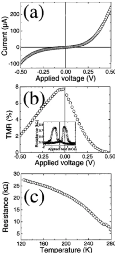
In order to perform the magneto-electrical characteriza-tion, junctions are defined in a cross-strip geometry through metallic contact masks. The path width is 200µm and each sample contains 14 tunnel junctions 200m⫻200m in size.17The resistance is measured with a standard two-probe dc technique, the positive voltage being applied on the top electrode. The average yield is about 50% of junctions with resistances exceeding the lead resistance by at least a factor of ten. At room temperature, the I共V兲 curves are nonlinear and symmetric and no evidence of TMR could be found even if electrodes have been shown to be magnetically decoupled using Kerr magnetometry. Nevertheless, I共V兲 were fitted us-ing the Brinkman formula20and a barrier height of 0.91 eV and a barrier thickness of 2.1 nm could be extracted. At 77 K, the I共V兲 curves are nonlinear and asymmetric 关Fig. 2共a兲兴 and the junction resistance varies between 6 and 25 k⍀. The voltage dependent current asymmetry, defined as
␣共V兲=I共+V兲/I共−V兲, increases with applied voltage when the
bottom electrode is positively biased and reaches 2–5 at 0.5 V. Furthermore, a TMR signal with values from 4% up to 8% could be observed关Fig. 2共b兲兴. The TMR versus applied volt-age characteristic, TMR共V兲, is asymmetric and, particularly interesting, the TMR maximum is shifted to the negative bias. This asymmetry can originate from a different Co–ZnO and ZnO– Co*interface smoothness but also from a different Co–ZnO and ZnO– Co* interface barrier height. Then, the
barrier height at Co–ZnO interface is less than the one at the ZnO– Co* interface. Finally, the temperatudependent re-sistivity, R共T兲, has been measured on those junctions. As shown by Akerman et al.,21this is the most reliable tunneling criteria. This last characteristic is reported in Fig. 2共c兲 for an applied voltage of 10 mV. No divergence of resistance could be observed as temperature is decreased. Then, elastic elec-tron tunneling remains the principal transport mechanism with respect to electron hopping inside the barrier.22 How-ever, the resistance varies by a factor of 5–10 and this large variation is beyond the one predicted from the smearing of the Fermi function as shown, for example, by Stratton.23
We thus have tried to understand these features using a simple model of the tunnel magnetoresistance. A parabolic bands approximation allows to simply solve the Schrödinger equation for an arbitrary potential and to take into account the composite nature of the barrier. The model we have used is described in Ref. 11 and is basically an extension of the approach proposed by Slonczewski24 including an exact nu-FIG. 1.共a兲 Low magnification TEM micrograph evidencing the continuity
of the ZnO barrier with a regular roughness;共b兲 HRTEM image evidencing the appearance of a 3 nm thick CoO layer located between the ZnO barrier and the bottom Co electrode.
FIG. 2.共a兲 Current versus voltage and 共b兲 magneto-resistance vs voltage at 77 K共inset: Resistance vs field兲; 共c兲 resistance vs temperature measured on a Glass– Ta共10 nm兲/Co共10 nm兲/ZnO共3 nm兲/Co共20 nm兲 tunnel junction.
merical resolution of the Schrödinger equation and a com-plete integration of the tunneling coefficient over all the states. The parameters used into the model are the thick-nesses of the CoO and ZnO layers, equal to 3 nm from the TEM pictures, and the barrier heights found in literature, equal to 0.6 eV for CoO25and 1 eV for ZnO.26Indeed, those parameters could not be extracted from fitting the I共V兲 curves as it is done commonly. To model the electrode bands, we used the parameters proposed by Davis et al.27 It appears clearly in Fig. 3 that all features described in Fig. 2 can be fairly reproduced and especially I共V兲 and TMR共V兲 asymme-tries. Changing slightly barrier heights and/or thicknesses does not modify drastically the shape of those curves but asymmetries are linked to the difference in barrier heights of the CoO and ZnO tunnel barriers. The low temperature fea-tures are thus well explained considering the composite na-ture of the barrier.
On the other hand, the lack of TMR and the symmetric I共V兲 curve at room temperature contrast with this picture. The important temperature dependance of the resistance, a factor of 5 between 300 and 77 K, indicates the existence of thermally activated modes of conduction. The effective pa-rameters deduced from the room temperature I共V兲 curves, fitted effective barrier height of 0.91 eV and a barrier thick-ness of 2.1 nm, could be interpreted as the one of a single ZnO barrier. This would imply that the thermally activated transport is mostly related to CoO which loses its insulating character at room temperature. This behavior has already been observed by Platt et al.25 The suppression of TMR at room temperature is then explained by the progressive tran-sition from a ferromagnetic Co bottom electrode with a CoO–ZnO barrier to a non polarized CoO electrode with a
ZnO barrier. Indeed, at room temperature, CoO is either an-tiferromagnetic or paramagnetic.
The good agreement between our low temperature ex-perimental data and the free electron model make us confi-dent in the prediction of this theoretical approach, which predicts we can achieve much higher asymmetry ratio by decreasing the CoO layer thickness. Indeed, the control of the bottom CoO layer thickness is the key to optimize the magnetic field dependent current–voltage characteristics of these rectifying diodes. The oxidation of the bottom elec-trode is caused of course by the atmosphere when the sample is transferred共and the metallic mask changed兲 but also and mainly by the oxygen reactive atmosphere during the ZnO deposition.
1
M. Jullière, Phys. Lett. 54A, 225共1975兲.
2
J. Zhang, R. M. White, J. Appl. Phys. 83, 6512共1998兲; J. Nassar, M. Hehn, A. Vaurès, F. Petroff, and A. Fert, Appl. Phys. Lett. 73, 698共1998兲.
3
M. Tsunoda, K. Nishikawa, S. Ogata, and M. Takahashi, Appl. Phys. Lett. 80, 3135共2002兲.
4
W. Zhu, C. J. Hirschmugl, A. D. Laine, B. Sinkovic, and S. S. P. Parkin, Appl. Phys. Lett. 78, 3103共2001兲; M. F. Gillies, A. E. T. Kuiper, J. B. A. van Zon, and J. M. Sturm, ibid. 78, 3496共2001兲; J. S. Moodera, L. R. Kinder, T. M. Wong, R. Meservey, Phys. Rev. Lett. 74, 3273共1995兲.
5
M. Covington, J. Nowak, and D. Song, Appl. Phys. Lett. 76, 3965共2000兲; P. Rottländer, H. Kohlstedt, P. Grünberg, and E. Girgis, J. Appl. Phys. 87, 6067共2000兲.
6
H. Boeve, J. De Boeck, and G. Borghs, J. Appl. Phys. 89, 482共2001兲; J. J. Sun, K. Shimazawa, N. Kasahara, K. Sato, S. Saruki, T. Kagami, O. Redon, S. Araki, H. Morita, and M. Matsuzaki, Appl. Phys. Lett. 76, 2424
共2000兲. 7
S. Tanoue and A. Yamasaki, J. Appl. Phys. 88, 4764共2000兲.
8
R. S. Beech, J. Anderson, J. Daughton, B. A. Everitt, and D. Wang, IEEE Trans. Magn. 32, 4713共1996兲; T. S. Plaskett, P. P. Freitas, J. J. Sun, R. C. Sousa, F. F. da Silva, T. T. P. Galvao, N. M. Pinho, S. Cardoso, M. F. da Silva, and J. C. Soares, Proceedings of the Mat. Res. Soc. Conference, Symp. M, Spring共1997兲.
9
C. L. PLatt, B. Dieny, and A. E. Berkowitz, Appl. Phys. Lett. 69, 2291
共1996兲. 10
T. S. Plaskett and P. P. Freitas, J. Appl. Phys. 76, 6104共1994兲.
11
F. Montaigne, M. Hehn, and A. Schuhl, Phys. Rev. B 64, 144402共2001兲.
12
C. Tiusan, M. Chshiev, A. Iovan, V. da Costa, D. Stoeffler, T. Dimopoulos, and K. Ounadjela, Appl. Phys. Lett. 79, 4231共2001兲.
13
T. Mitsuyu, S. Ono, and K. Wasaj, J. Appl. Phys. 51, 2464共1980兲.
14
R. G. Heideman, P. V. Lambeck, and J. G. E. Gardeniers, Opt. Mater.
共Amsterdam, Neth.兲 4, 741 共1995兲. 15
T. K. Subramanyam, B. Srinivasulu Naidu, and S. Uthanna, Opt. Mater.
共Amsterdam, Neth.兲 13, 239 共1999兲. 16
T. Dietl, H. Ohno, F. Matsukura, J. Cibert, and D. Ferrand, Science 287, 1019共2000兲; J.-J. Wu, S.-C. Liu, and M.-H. Yang, Appl. Phys. Lett. 85, 1027共2004兲.
17
M. Hehn, O. Lenoble, D. Lacour, C. Féry, M. Piécuch, C. Tiusan, and K. Ounadjela, Phys. Rev. B 61, 11643共2000兲.
18
T. Lamara, M. Belmahi, O. Elmazria, L. Le Brizoual, J. Bougdira, M. Rémy, and P. Alnot, Diamond Relat. Mater. 13, 581共2004兲.
19
L. Smardz, U. Köbler, and W. Zinn, J. Appl. Phys. 71, 5199共1992兲.
20
W. F. Brinkman, R. C. Dynes, and J. M. Rowell, J. Appl. Phys. 41共5兲, 1915共1970兲.
21
J. J. Akerman, R. Escudero, C. Leighton, S. Kim, D. A. Rabson, R. W. Dave, J. M. Slaughter, and I. K. Schuller, J. Magn. Magn. Mater. 204, 86
共2002兲. 22
Y. Xu, D. Ephron, and M. R. Beasley, Phys. Rev. B 52, 2843共1995兲.
23
R. Stratton, Phys. Chem. Solids 23, 1177共1962兲.
24
J. C. Slonczewski, Phys. Rev. B 39, 6995共1989兲.
25
C. L. Platt, A. S. Katz, E. P. Price, R. C. Dynes, and A. E. Berkowitz, Phys. Rev. B 61, 68共2000兲.
26
L. F. Lou, J. Appl. Phys. 50, 555共1979兲.
27
A. H. Davis and J. M. MacLaren, J. Appl. Phys. 87, 5224共2000兲. FIG. 3. 共a兲 Current vs voltage and 共b兲 magneto-resistance vs voltage
com-puted in the free electron model on a CoO–ZnO composite tunnel barrier using thicknesses extracted from TEM images and barrier heights found in literature.