Science Arts & Métiers (SAM)
is an open access repository that collects the work of Arts et Métiers Institute of
Technology researchers and makes it freely available over the web where possible.
This is an author-deposited version published in:
https://sam.ensam.eu
Handle ID: .
http://hdl.handle.net/10985/17935
To cite this version :
Magdalena G. NISTOR, Nicolae Bogdan MANDACHE, Jacques PERRIÉRE, Christian HÉBERT,
Florin V. GHERENDI, Wilfried SEILER - Growth, structural and electrical properties of polar ZnO
thin films on MgO (100) substrates - Thin Solid Films - Vol. 519, n°11, p.3959-3964 - 2011
Any correspondence concerning this service should be sent to the repository
Administrator :
archiveouverte@ensam.eu
Growth, structural and electrical properties of polar ZnO thin
films on
MgO (100) substrates
M. Nistor
a,⁎
, N.B. Mandache
a, J. Perrière
b, C. Hebert
b, F. Gherendi
a, W. Seiler
ca
National Institute for Lasers, Plasma and Radiation Physics, Plasma Physics and Nuclear Fusion Laboratory, L22 P.O. Box. MG-36, 77125 Bucharest-Magurele, Romania
bInstitut des Nanosciences de Paris, Université Pierre et Marie Curie-Paris 6, CNRS UMR 7588, Campus Boucicaut, 140 rue de Lourmel, 75015 Paris, France c
Laboratoire d'Ingenierie des Materiaux, Ecole Nationale Supérieure des Arts et Métiers, CNRS UMR 8006, 151 Boulevard de l'Hopital, 75013 Paris, France
a b s t r a c t
Keywords:
Epitaxial zinc oxide thinfilms Metal-semiconductor transition Pulsed-electron beam deposition Channel-spark
ZnOfilms have been grown on (100) oriented MgO substrates by pulsed-electron beam deposition in the room temperature to 500 °C range. Highly (00·2) texturedfilms are obtained for a growth temperature higher than 200 °C, and epitaxialfilms are formed at 500 °C with the following epitaxial relationships: (1-1·0)ZnO// (110)MgO
and (11·0)ZnO// (110)MgO, despite the difference in symmetry betweenfilm and substrate. The low temperature
resistivity curves evidenced a metal–semiconductor transition for the ZnO films grown in the 300 to 500 °C range which has been interpreted in the frame of the model of conductivity in disordered oxides.
1. Introduction
While the growth of c-axis epitaxial ZnO films on crystalline substrates like sapphire presenting the rhomboedral symmetry has been and is nowadays the subject of numerous works [1], the formation of ZnO films on single crystal substrates presenting a different structural symmetry is not so well documented. The formation of non polar ZnOfilms, i.e. ZnO films with their c-axis in the plane parallel to the substrate, would however lead to interesting applications[2,3]. Motivated by this aspect, the growth of ZnOfilms on cubic substrates has been studied, in particular on SrTiO3single
crystal substrates according to the fact that a high density, two dimensional electron gas with unique electrical and thermal proper-ties forms at the interface between SrTiO3and other oxides[3,4]. The
growth of non polar m oriented (11·0) ZnOfilms on (001) SrTiO3
substrates has been thus reported [3,4], while the classical polar (00·2) ZnO growth is observed on (111) oriented SrTiO3[5].
In the case of ZnOfilms on MgO single crystal substrates, the situation appears rather confusing, with results which in terms offilm orientation not only depend upon the substrate orientation, but also on the growth method, and experimental conditions. Indeed,films with multiple textures, or m-axis or c-axis oriented ZnOfilms can be obtained depending upon growth parameters[2,6–8]. This underlines
the difficulties to obtain high crystalline quality ZnO thin films with a single epitaxial relationship with the MgO single crystal substrate. The epitaxial growth is not trivial, due to differences in crystallographic symmetries of the hexagonal ZnO network (a = 0.3249 nm and c = 0.5206 nm) and the cubic MgO (a = 0.421 nm).
We have studied the formation, structure and electrical properties of ZnOfilms grown on (100) oriented single crystal MgO substrates, by the pulsed-electron beam deposition method (PED). This thinfilm growth technique[9–13], conceptually similar to the pulsed laser deposition, differs by the use of an intense pulsed electron beam to ablate the target material instead of a laser beam. Oxidefilms are easily grown by PED, with a good control of the surface morphology, cationic composition, oxygen stoichiometry and crystalline structure of thefilms[9–14]. Our main objective was to determine the pertinent parameters governing the ZnOfilm orientation and epitaxial relation-ships with MgO substrates, and to correlate their structural char-acteristics with their electrical properties. We evidenced the (00·2) ZnO growth on (100) MgO substrates, as well as the heteroepitaxial growth of ZnO films. Depending on the growth temperature, variations in the electrical properties were observed for the ZnO films grown on (100) MgO substrates. The resistivity curve shows a semiconducting behaviour for thefilms grown at room temperature, while thefilms grown in the 300 to 500 °C range show a metallic conductivity at room temperature followed at lower temperatures by a metal–semiconductor transition (MST), as was already observed in epitaxially ZnOfilms on Al2O3single crystal substrates grown by PED
[14]. This behaviour was interpreted in the frame of the quantum corrections to conductivity in a disordered medium[15].
⁎ Corresponding author. Tel./fax: +40 214574490. E-mail address:mnistor@infim.ro(M. Nistor).
2. Experimental details
The ZnOfilms were grown on (100) oriented MgO substrates by the PED method[9,16,17]. The PED set-up consists of a pulsed electron beam source in the channel-spark discharge configuration and a vacuum chamber for the thin film growth. The channel-spark discharge configuration consists of a hollow cathode, a dielectric capillary tube (6 mm diameter and 100 mm length) and the vacuum chamber as the grounded anode.
A pulsed intense electron beam is produced when an external capacitor of 16 nF, charged at 15 kV, is discharged between the hollow cathode and the anode. The pulsed electron beam has 100 ns full width at half maximum (FWHM), a fluence of 2.5 J/cm2 and a
repetition rate of 1 Hz. The electron beam interacts at an angle of 45° with the ZnO target, in Ar gas at a pressure of 1 Pa and a residual oxygen pressure equal to 10−3Pa. The MgO (100) substrates were placed parallel to the target at a distance of 40 mm. ZnO thinfilms were grown under a controlled substrate temperature in the room temperature to 500 °C range. After deposition thefilms were cooled down under the argon pressure used for the growth.
The thickness and composition of thefilms were measured by Rutherford backscattering spectrometry (RBS) using the 2 MeV Van de Graaff accelerator at the Institut des Nanosciences de Paris (Université Paris 6). The structural characterizations of the ZnO films were carried out by X-ray diffraction (XRD) analyses using a four-circle diffractometer (Philips Xpert MRD) with the Cu Kα radiation (λ=0.154 nm) at the Laboratoire d'Ingenierie des Materi-aux (Ecole Nationale Supérieure des Arts et Métiers). Analyses in the symmetric Bragg–Brentano geometry were used to determine the axis parameters and possible textures of thefilms. The in-plane epitaxial relationships between the ZnOfilms and MgO substrates were studied by asymmetric X-ray diffraction from the measurements of pole figures for selected XRD peaks of the films and substrate. The resistivity of ZnOfilms as a function of temperature (from room T down to liquid He) was obtained by the standard dc four-probe measurements.
3. Results
The parameters of the PED method were optimized in order to obtain dense and smooth ZnOfilms free from any particulates at their surface, as it has been previously established [9], with the film thickness in the 50–100 nm range.Fig. 1 represents a typical RBS spectrum which shows the formation of a stoichiometric and uniform ZnOfilm. However, due to the accuracy of the RBS analysis for the determination of the content in light elements (like oxygen), i.e. about 5%, we cannot exclude a slight oxygen deficiency in the ZnO films. Such a possible deviation in stoichiometry could be due to the fact that thesefilms are grown under a quite low oxygen pressure that usually involves an unbalanced incorporation of cations and oxygen atoms into thefilm[18,19]. This RBS spectrum does not show the presence of elements other than Zn, O and Mg, i.e. the incorporation during the PED growth of foreign atoms which could play an important role in the transport properties of thefilms[20,21]is not evidenced by RBS.
X-ray diffraction patterns were recorded for the ZnOfilms grown on (100) MgO substrates at room T, 300 and 500 °C. Films grown at Tb200 °C were found amorphous.Fig. 2shows typical XRD patterns for films grown at 300 and 500 °C and for the MgO substrate, respectively. The scan shows the presence of the (00·2) reflection peak and its harmonics characteristic of the ZnO wurtzite structure, along with the (100) MgO substrate reflections, indicating that the ZnOfilm is highly c-axis oriented, a very small (10·0) ZnO peak being observed only at 2θ=31.7°. Note that the (111), (200), (220) and (311) Au peaks observed in the XRD pattern of the ZnOfilm are due to the Au contacts deposited on thefilm for resistivity measurements.
Moreover, the absence of any additional peaks in the XRD patterns rules out the presence of spurious crystalline phases in the ZnOfilms. The c-axis parameters obtained from the XRD patterns, the values of crystallite size d (coherence length) deduced from the (00·2) ZnO line width (the Scherrer formulae) and the FWHM values of the rocking curves of the (00·2) reflection peaks are presented inTable 1 for the ZnO films grown on MgO substrates at 300 and 500 °C substrate temperatures. The FWHM of the (00·2) ZnO rocking curves show a decrease from 4.8° at 300 °C to 2.4° at 500 °C. Moreover, the ZnO c axis values are larger than the bulk value (0.5206 nm), the difference decreasing with increasing growth temperature, which could be explained by a decreasing defect density in thefilms as the growth temperature increases. All these results prove an enhance-ment of the crystalline quality of the ZnOfilms with T, i.e. a decrease of the defect density infilms with increasing growth T, as it is generally observed in the case of ZnOfilm growth[1,14,22].
XRD polefigures were observed only for films grown at TN300 °C. Fig. 3 represents a typical pole figure of the (10·3) ZnO plane, recorded for 2θ=62.8°, for a ZnO thin film grown on the (100) MgO substrate at 500 °C. Twelve well-defined poles are observed at a declination angleψ equal to 31.6°, i.e. the value expected for the (10·3) plane of the ZnO wurtzite structure in the case of a (00·2) texture. In addition, the poles located atψ=45° with a four fold
Fig. 1. A typical RBS spectrum recorded for a ZnOfilm grown by PED on the (100) MgO substrate at 300 °C.
Fig. 2. X-ray diffraction patterns for the ZnO thinfilms grown on the (100) MgO substrate at 300 and 500 °C and the (100) MgO substrate, respectively. The (111), (200), (220) and (311) Au peaks are marked by *.
symmetry (Fig. 3) correspond to the (220) plane of the MgO substrate, and are observed owing to the diffraction angle 2θ=62.8° of this plane.
The azimuthal positions of the (10·3) ZnO poles in respect with the MgO substrate (110) poles lead to the following in-plane relationships:
1−1·0
ð ÞZnO== 110ð ÞMgO and ð11·0ÞZnO== 110ð ÞMgO:
Owing to the six-fold in plane symmetry of the ZnO, these two relationships lead to the 12 poles which are observed inFig. 3. To highlight these epitaxial relationships,Fig. 4a and b represents the in-plane atomic arrangement corresponding to the interface (00·2) ZnO film on the (100) MgO substrate. In this schema, we have taken into account the rumpling phenomenon on the MgO surface. Indeed the MgO substrate heated under reduced oxygen pressure can undergo a rumpling phenomenon, i.e. atomic displacements of the O versus Mg atoms of the free surface plane, leading thus to the formation of an oxygen atomic plane at the surface[23]. The last MgO plane can thus be considered as an electronegative plane, and it has been schematized inFig. 4by the oxygen atoms of the (100) MgO plane. Accordingly, thefirst deposited ZnO plane is an electropositive plane, i.e. a (00·2) Zn plane has been thus considered in thesefigures.
The epitaxial relationships presented inFig. 4can be explained in the frame of the domain matching epitaxy or extended atomic distance mismatch approach[24], in which the m lattice units of the film match with p lattice units of the substrate. The values of m and p are defined as the minimum integers which satisfy the relation: m dZnO= p dMgO or dZnO= dMgO≈p = m
with dZnOand dMgObeing the respective atomic distances in the ZnO
and MgO parallel directions. The corresponding lattice mismatchδ can then be defined by:
δ = 2 m dZnO−p dMgO
h i
= m dZnO+ p dMgO
h i
:
Considering the two aligned directions inFig. 4, and the values of dZnOalong the (1-1·0) and (11·0) directions (0.2814 and 0.3249 nm
respectively), to compare with dMgO (0.5954 nm), the resulting
matching and lattice mismatches are given inTable 2. The limited values of the lattice mismatch along the two directions inFig. 4can justify the epitaxial relationships observed in this work.
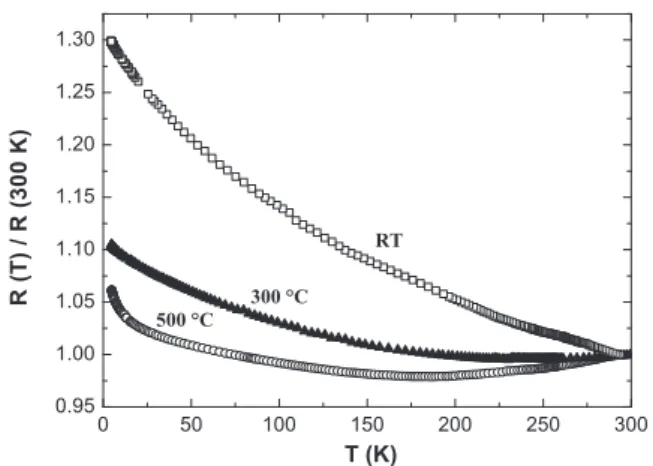
In order to check how the growth of ZnOfilms on (100) MgO single crystal substrates influence the electrical properties of the films, temperature variable resistivity measurements were performed.Fig. 5 shows the normalized resistance (R(T)/R(300 K)) measured in the temperature range 4–300 K for films grown at room T, 300 and 500 °C, respectively. The absolute values of resistivities measured at 300 K are: 0.0122Ωcm for the ZnO/MgO film grown at RT; 0.0033 Ωcm for the ZnO/MgOfilm grown at 300 °C and 0.0023 Ωcm for the ZnO/MgO film grown at 500 °C.
Thefilm grown at room T shows only a negative coefficient of R(T) which is characteristic of semiconducting behaviour. On the contrary, minima are observed on the curves corresponding to the 300 and 500 °C growth temperatures. In fact, from room T to the normalized resistance minimum, the temperature coefficient of resistivity is
positive (metallic behaviour), while for the lowest T it is negative (semiconducting behaviour). Such a metal–semiconductor transition has been reported for ZnOfilms doped with various elements, grown by different deposition methods [20,21,25–30], but pure undoped ZnO films grown with the same methods and same experimental conditions did not present such a metal–semiconductor transition (MST). Recently, a metallic behaviour and a MST have been reported in undoped ZnOfilms grown on c-cut sapphire substrates by PED[14], spray pyrolysis[30], the transition temperature being at about 170 K and around 420 K, respectively.
Fig. 3. Polefigure of the (10·3) ZnO plane for the ZnO film grown on the (100) MgO substrate at 500 °C.
Fig. 4. Schematic representation of the interface between the (00.2) ZnOfilm and the (100) MgO substrate with the corresponding in-plane relationships: (a) [1-1·0]ZnO// [110]MgO
and (b) [11·0]ZnO// [110]MgO.
Table 1
Structural parameters of the ZnOfilms grown at 300 and 500 °C on (100) MgO substrates. Substrate temperature C-axis parameter (nm) Crystallite size (nm) FWHM rocking curve (°) 300 °C 0.5307 14 4.8 500 °C 0.5253 28 2.4
Fig. 6a shows the Arrhenius plot of the resistivity of the ZnOfilm grown on a MgO substrate at room T. As it is shown in the inset, in the temperature range 294 to 185 K (ΔT=109 K) the resistivity follows an Arrhenius law versus temperature written in the form: lnρ=lnρ0+ (Ea/
kB) T−1, and the estimated activation energy is Ea= 2.65 meV. For
Tb185 K the resistivity increases and a pronounced curvature is observed in the Arrhenius plot, as it is generally observed in semiconducting oxides[19]. A classical explanation of this behaviour is based on a variable range hopping (VRH) mechanism related to the localization of carriers, in which lnρ (T) follows a linear dependence on T−1/4(three dimensional VRH)[19]. However, this does not seem to be the case for the ZnOfilm grown at room T. Actually, as it is shown in Fig. 6b, lnρ (T) does not present a linear variation with T−1/4on a
significant temperature range thus a VRH mechanism does not seem to be the dominant mechanism in this low temperature domain.
The MST observed in the curve corresponding to ZnOfilms grown at 300 and 500 °C (Fig. 5) could be due to a variation with the temperature of the carrier density[28,29]. The density and mobility of carriers were determined by Hall effect measurements. However, the density and mobility of carriers were determined with a rather poor accuracy (about 10%), i.e. of the order of the resistivity variation due to the MST. So even if the carrier density was found roughly constant between 80 and 300 K and equal to 1.95 × 1020cm−3(for the ZnOfilm
grown at 500 °C), it is not possible to a priori exclude that the MST is due to a change in the carrier concentration. However another explanation can be envisaged, similar to that proposed in the case of ZnOfilms grown on sapphire substrates[14]. As a result, the specific behaviour of the R(T) curves corresponding to the ZnOfilms grown at 300 and 500 °C was analyzed in the frame of the quantum corrections to conductivity in a disordered conductor[15]. Indeed, the metallic conductivity followed at a low temperature by a metal–semiconductor transition can originate from the weak localization and electron– electron interactions effects which are known to occur in a disordered conductor[16]. Such an approach has been already used to explain the crossover from semiconductor to metallic behaviour in various oxide materials like SrRuO2[31], LaNiO3[31,32]or even ZnO[14,21,27].
In this approach, the changes in conductivity have been analyzed and modelled[32]and the resistivity of oxidefilms can be described by the following expression:
ρ Tð Þ = 1
σ0+ a1Tp= 2+ a2T1= 2
+ bT2 ð1Þ
whereσ0is related to the residual resistivity (σ0= 1/ρ0); a1Tp/2and
a2T1/2are the quantum corrections corresponding respectively to the
weak localization effect (a1Tp/2) and Coulomb interaction effect (a2T1/2)
in the case of a 3D dimension disordered oxidefilm[32]; and bT2is the
usual Boltzmann term. The value of p depends on the type of the interactions, p being 2 for electron–electron and 3 for electron–phonon interactions, respectively.
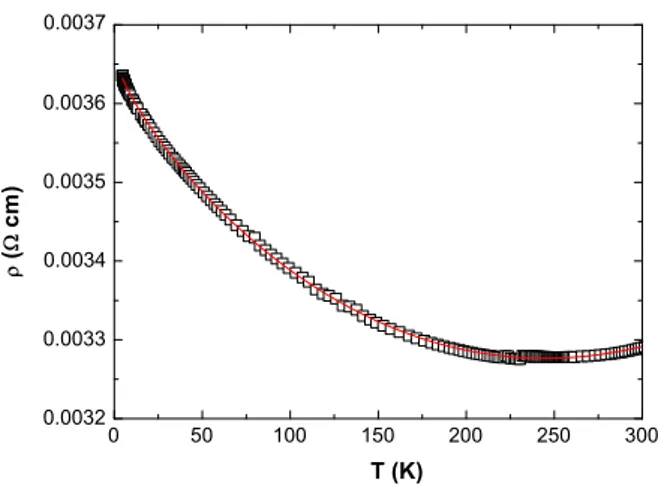
The resistivity curves for ZnOfilms grown on MgO substrates at 300 and 500 °C, respectively werefitted with the Eq.(1), as shown inFigs. 7 and 8and thefit parameters are given inTable 3. Owing to thefilm thickness (N50 nm), the fit indicates that the 3D approach (Eq.(1)) describes correctly theρ (T) behaviour for both films. Moreover, we have checked that theρ (T) variation could not be described by a log (T) variation predicted for a 2D dimensional disordered system[15].
The parameter a1is very small compared with a2, and it is a clear
indication that the Coulomb interaction represents the most important contribution in the quantum corrections to conductivity in disordered oxidefilms as it has been previously reported[27,31,32].
The model of quantum corrections to conductivity is valid when the Fermi wavelengthλF(2π / (3π2n)1/3) and the electronic mean free path Fig. 5. Normalized resistance as a function of temperature for ZnO thinfilms grown on the (100) MgO substrate at room T, 300 and 500 °C.
a
b
Fig. 6. a. Arrhenius plot of the normalized resistance of a ZnO thinfilm grown on the (100) MgO substrate at room T. The inset shows the variation in the 294 to 185 K range on an expanded scale. b. The variation of the lnρ in function of T−1/4.
Table 2
The domain matching epitaxy relationships and the lattice mismatch for the corresponding in-plane orientations of the ZnOfilms on the (100) MgO substrate.
In-plane orientation Domain matching epitaxy relationships
Lattice mismatch
(1-1·0)ZnO// (110)MgO 2 dZnO≈1 dMgO δ=5.60%
Λ (h / ρne2λ
F) are comparable, where n is the carrier density,ρ the
resistivity and e the electron charge[14,32]. In this work, with the values of resistivity (ρ) and electron density (n) measured by Hall effect measurements at room T for the ZnO film grown at 300 °C (ρ=0.0033 Ωcm, μ=12.94 Vcm2
/s and n = 1.45 × 1020cm−3) and 500 °C (ρ=0.0023 Ωcm, μ=14.12 Vcm2/s and n = 1.95 × 1020cm−3)
the validity of the model was checked,λFandΛ being comparable
(λF 300= 3.9 nm,Λ300= 1.9 nm andλF 500= 3.5 nm,Λ500= 1.7 nm,
respectively).
This model leads to a relatively high value of the transition temperature corresponding to the minimum of the resistivity (Tm= 240 K for the ZnOfilm grown at 300 °C and 186 K for the ZnO
film grown at 500 °C) but similar values of the Tmwere already reported
for other oxidefilms: Ga doped ZnO (Tm= 170 K)[21], B doped ZnO
(Tm= 120 K)[27], undoped ZnO (Tm= 170 K)[14], indium-tin oxide
(Tm= 175 K)[33]and non-polar ZnOfilms[34]. In order to check the
validity of the model at such higher Tmthe quantum corrections were
compared to the Boltzmann conductivity in the range 10–250 K (δσ=a1Tp/2+ a2T1/2bb σ0). The values of the quantum corrections
obtained from thefit (Fig. 8) give a ratioδσ/σ0b0.1 and are much smaller
than the values corresponding to the Boltzmann conductivity[32]. The fact that the Boltzmann conductivity variation with temperature (bT2
term) is very limited in this temperature range (due to the low b value deduced from thefit) leads to a variation of the Boltzmann conductivity lower than 1% in the 10–250 K range. So, even with limited values, the
quantum corrections can overcome this low variation in Boltzmann conductivity and can lead to the high transition temperature Tm.
4. Discussion
The ZnOfilms grown by PED on MgO substrates show a preferred c-axis orientation, while the published results on ZnOfilms grown by other methods report a wide variety of orientations [2,6–8]. The strong (00·2) texture observed in this work has to be explained and in this aim, the effects of the surface free energy have to be considered. Indeed, if γf, γs and γi are the free energy for the film–ambient,
substrate–ambient and film–substrate interface respectively, and γe
the epitaxial energy gain, the increase of surface free energy due to the presence of thefilm is given by:
G =ðγf−γsÞ + γð i−γeÞ
and thefilm grows in a way to minimize the free energy G[35]. First, the (00·2) ZnO texture was observed in films presenting or not epitaxial relationships with the MgO substrates. The termγedoes not
seem thus to play a major role on the ZnOfilm texture.
In the ZnO wurtzite structure, the (00·2) plane is a polar plane, i.e. alternate planes of Zn and O. The surface free energy of such planes will diverge as it has been shown[36]. By comparison the prismatic planes of this wurtzite structure have a lower surface free energy. In a first approach, solely based on energy considerations, the growth of ZnOfilms should occur with a prismatic plane ((10·0) or (11·0) for example) parallel to the substrate surface, whatever be the substrate. However, kinetics effects are present during thefilm formation, and the very high growth rate of ZnO along the c-axis leads to a columnar growth for ZnO which is observed on various substrates[1,37], despite the unfavourable surface free energy of the (00·2) plane. On the contrary, the (10·0) or (11·0) ZnO texture would lead to a 2D like growth, i.e. a platelet like structure, and should only be obtained in the case of a low growth rate or deposition rate. These conditions are fulfilled in the growth by molecular beam epitaxy, and the formation of m oriented ZnOfilms on MgO substrates has been reported in these conditions[7]. A highflux of incident species on the substrate, which is a characteristic of the pulsed deposition methods, will favour a high growth rate and therefore the formation of polar (00·2) ZnOfilms can be expected by PED.
Another important factor can play a role on the precise ZnOfilm texture, i.e. the rumpling phenomenon described above. This phenomenon will be equivalent to the creation of an electronegative surface plane (polar plane), which will result in the deposition of an electropositive Zn plane, i.e. a polar plane as the (00·2) ZnO plane. This explanation of the ZnO film orientation related to the polar nature of the substrate surface is very similar to what was recently proposed in the growth of ZnO on SrTiO3substrates[3,4]. Generally,
non polar (11·0) oriented ZnOfilms are grown on (001) oriented SrTiO3substrates, however a c-axis columnar growth is observed on
etched (001) oriented SrTiO3substrates. This change in ZnO growth
direction is believed to be caused by the change of SrTiO3polarity
induced by the etching[5].
The metallic conductivity observed in the ZnO films can be explained by the formation of a degenerate band appearing in heavily doped semiconductors [20,38]. Hall measurements performed on thesefilms gave carriers densities in the 1020
cm−3ranges, i.e. values sufficient to give rise to this effect[39]. In addition, the crossover from metallic to semiconducting behaviour has been interpreted by the quantum corrections to conductivity in disordered conductors[15]. The two pertinent points for the occurrence of MST are thus a sufficient high density of carriers and a sufficient density of structural defects in thefilms. In the case of ZnO films doped by various elements [20,21,25–27], the density of carriers is related to the presence of dopants. In the present case, noticeable incorporations of foreign
Fig. 7. Temperature dependence of the resistivityρ(T) of ZnO grown on the (100) MgO substrate at 300 °C by PED. The solid line is thefit with the Eq.(1)of the experimental data (open rectangles).
Fig. 8. Temperature dependence of the resistivityρ(T) of ZnO grown on the (100) MgO substrate at 500 °C by PED. The solid line is thefit with Eq.(1)of the experimental data (open rectangles).
atoms in the ZnOfilms has not been evidenced, but owing to the sensitivity of RBS analysis, we cannot a priori exclude that a very small amount of elements is present and could thus contribute to the high density of carriers. On the other hand, even if measurable oxygen deficiencies have not been evidenced by RBS, the oxygen pressure during the growth, estimated around 10−3Pa would be sufficiently low to lead to limited oxygen incorporation in thefilms[18], i.e. to the presence of oxygen vacancies. This oxygen deficiency can explain the rather high carrier densities determined by Hall effect measurements (about 1020cm−3) in thesefilms.
One part of the disorder in the PED grown ZnOfilms may be related to the oxygen vacancies due to the growth process. Indeed, these oxygen vacancies could be at least partly at the origin of ZnO cell distortion in thefilms. Moreover, the high deposition rates observed in PED[9], which plays a role on thefilm growth texture (see above), can also be at the origin of the disorder created in the ZnOfilms. Indeed, deposition rates as high as 1 nm per pulse are currently obtained during PED growth, thanks to the high efficiency of energy transfer from incident polyenergetic (up to 15 keV) electrons to the ZnO target. For comparison purposes, ten times lower deposition rates are obtained during another pulsed deposition process, pulsed laser deposition. With such high deposition rates, the crystalline quality of the grownfilms cannot be guaranteed, as it can be checked through the difference in ZnO axis parameter with bulk value, width of the diffraction peak and FWHM values of the (00·2) rocking curve, observed in this work.
5. Conclusions
In summary, the pertinent factors allowing the formation by PED of (00·2) rhombohedral ZnO texturedfilms on (100) MgO substrates are (i) the high deposition rate (high flux of incident species) favouring the high (00·2) ZnO growth rate, and (ii) the rumpling phenomenon of the MgO substrate favouring the growth of the polar (00·2) ZnO plane at the surface of the substrate. The high density of crystalline defects in the ZnOfilms grown on (100) oriented MgO substrates over the 300–500 °C temperature range associated with the high deposition rate of the PED method is very favourable for the occurrence of the metal–semiconductor transition observed in the variable temperature resistivity curves.
Acknowledgements
The authors gratefully acknowledgefinancial support from the Romanian Ministry for Education, Research, Youth and Sport (Project No. 12-112/2008) and from the agreement on cooperation between INSP, Université Pierre et Marie Curie-Paris 6 and NILPRP.
References
[1] S.J. Pearton, D.P. Norton, K. Ip, Y.W. Heo, T. Steiner, Prog. Mater. Sci. 50 (2005) 293. [2] L.C. Nistor, C. Ghica, D. Matei, G. Dinescu, M. Dinescu, G.V. Tandeloo, J. Cryst.
Growth 277 (2005) 26.
[3] C.H. Jia, Y.H. Chen, G.H. Liu, X.L. Liu, S.Y. Yang, Z.G. Wang, J. Phys. D Appl. Phys. 42 (2009) 015415.
[4] M. Karger, M. Schilling, Phys. Rev. B 71 (2005) 075304.
[5] X.H. Wei, Y.R. Li, J. Zhu, W. Huang, Y. Zhang, W.B. Luo, H. Ji, Appl. Phys. Lett. 90 (2007) 151918.
[6] F.K. Shan, G.X. Liu, W.J. Lee, B.C. Shin, Integr. Ferroelectr. 78 (2006) 181. [7] E. Cagin, J. Yang, W. Wang, J.D. Phillips, S.K. Hong, J.W. Lee, J.Y. Lee, Appl. Phys. Lett.
92 (2008) 233505.
[8] M.W. Cho, A. Setiawan, H.J. Ko, S.H. Kong, T. Yao, Semicond. Sci. Technol. 20 (2005) S13. [9] M. Nistor, N.B. Mandache, J. Perrière, J. Phys. D Appl. Phys. 41 (2008) 165205. [10] R.J. Choudhary, S.B. Ogale, S.R. Shinde, V.N. Kulkarni, T. Venkatesan, K.S.
Harshavardhan, M. Strikovski, B. Hannoyer, Appl. Phys. Lett. 84 (2004) 1483. [11] M. Nistor, P. Charles, M. Ganciu, M. Lamoureux, N.B. Mandache, A.M. Pointu,
Plasma Sources Sci. Technol. 11 (2002) 183.
[12] M. Nistor, F. Gherendi, M. Magureanu, N.B. Mandache, A. Ioachim, M.G. Banciu, L. Nedelcu, M. Popescu, F. Sava, H.V. Alexandru, Appl. Surf. Sci. 247 (2005) 169. [13] M. Nistor, J. Perrière, C. Hebert, W. Seiler, J. Phys. Condens. Matter 22 (2010)
045006.
[14] M. Nistor, F. Gherendi, N.B. Mandache, C. Hebert, J. Perrière, W. Seiler, J. Appl. Phys. 106 (2009) 103710.
[15] P.A. Lee, T.V. Ramakrishnan, Rev. Mod. Phys. 57 (1985) 287. [16] M. Nistor, N.B. Mandache, J. Optoelectron. Adv. Mater. 7 (2005) 1619. [17] M. Nistor, F. Gherendi, M. Magureanu, N.B. Mandache, J. Optoelectron. Adv. Mater.
7 (2005) 979.
[18] R. Perez-Casero, A. Gutierrez-Llorente, O. Pons-Y-Moll, W. Seiler, R.M. Defourneau, D. Defourneau, E. Millon, J. Perrière, J. Appl. Phys. 97 (2005) 054905.
[19] R. Perez-Casero, J. Perrière, A. Gutierrez-Llorente, D. Defourneau, E. Millon, W. Seiler, L. Soriano, Phys. Rev. B 75 (2007) 165317.
[20] V. Bhosle, A. Tiwari, J. Narayan, Appl. Phys. Lett. 88 (2006) 032106. [21] V. Bhosle, A. Tiwari, J. Narayan, J. Appl. Phys. 100 (2006) 033713.
[22] V. Craciun, R.K. Singh, J. Perrière, J. Spear, D. Craciun, J. Electrochem. Soc. 147 (2000) 1077.
[23] D.R. Alfonso, J.A. Snyder, J.E. Jaffe, A.C. Hess, M. Gutowski, Phys. Rev. B 62 (2000) 8318. [24] J. Narayan, K. Dovidenko, A.K. Sharma, S. Oktyabarsky, J. Appl. Phys. 84 (1998)
2597.
[25] O. Bamiduro, H. Mustafa, R. Mundle, R.B. Konda, A.K. Pradhan, Appl. Phys. Lett. 90 (2007) 252108.
[26] A.K. Pradhan, L. Douglas, H. Mustata, R. Mundle, D. Hunter, C.E. Bonner, Appl. Phys. Lett. 90 (2007) 072108.
[27] X.D. Liu, E.Y. Jiang, Z.Q. Li, J. Appl. Phys. 102 (2007) 073708.
[28] C. Fournier, O. Bamidoro, H. Mustafa, R. Mundle, R.B. Konda, F. Williams, A.K. Pradhan, Semicond. Sci. Technol. 23 (2008) 085019.
[29] Y. Li, C. Li, D. He, J. Li, J. Phys. D Appl. Phys. 42 (2009) 105303. [30] N. Kavasoglu, A.S. Kavasoglu, Phys. B 403 (2008) 2807.
[31] G. Herranz, F. Sánchez, B. Martínez, J. Fontcuberta, M.V. García-Cuenca, C. Ferrater, M. Varela, P. Levy, Eur. Phys. J. B 40 (2004) 439.
[32] W. Noun, B. Berini, Y. Dumont, P.R. Dahoo, N. Keller, J. Appl. Phys. 102 (2007) 063709. [33] T. Ohyama, M. Okamoto, E. Otsuka, J. Phys. Soc. Jpn 54 (1985) 1041.
[34] P. Pant, J.D. Budai, R. Aggarwal, R.J. Narayan, J. Narayan, Acta Mater. 57 (2009) 4426.
[35] O. Pons, Y. Moll, J. Perrière, E. Millon, R.M. Defourneau, D. Defourneau, B. Vincent, A. Essahlaoui, A. Boudrioua, W. Seiler, J. Appl. Phys. 92 (2002) 4885.
[36] P.W. Tasker, J. Phys. C Solid State Phys. 12 (1979) 4977.
[37] V. Craciun, J. Perrière, N. Bassim, R.K. Singh, D. Craciun, J. Spear, Appl. Phys. A 69 (1999) 531.
[38] N.F. Mott, Metal Insulator Transitions, Taylor and Francis, London, 1974. [39] A.P. Roth, J.B. Webb, D.F. Williams, Solid State Comm. 39 (1981) 1269. Table 3
Values of thefit parameters of Eq.(1)for ZnOfilms grown on (100) MgO substrates at 300 and 500 °C, respectively. Substrate temperature Fit parameters 1/ρ0(Ω−1cm−1) a1(Ω−1cm−1K−p/2) p a2(Ω−1cm−1K−1/2) B (Ω−1cm−1K−2) 300 °C 272.4 ± 0.05 0.2 ± 0.001 2 1.0 ± 0.02 3.6 × 10⁻⁹± 2.8 × 10⁻¹¹ 500 °C 419.2 ± 0.2 0.009 ± 0.0002 3 2.1 ± 0.04 4.0209 × 10⁻⁹± 4.9 × 10⁻¹¹