3 Acknowledgements:
As with any large work there are many people to thank, first and foremost my thanks go to my wonderful wife Bec, you are my muse and we have made it through this great adventure we set out on. Maybe not in the way we thought we would but the important thing is we made it! Secondly I’d like to thank my parents, as ‘The Herd’ say I am the sum of it all, and at this stage the majority of my time on earth has been guided by your advice, be it comedic, direct, soft or stern. Both of you have helped to mould me into the man I am. I would like to thank my sister as well for encouraging me to chase my dreams and thanks for all the support from B, Carolyn, Andrew, Dan and Basti the best in laws I could ask for.
Many thanks go to both my supervisors Daniel and Duy, it has been a challenging project to pull together over the past three years. The research meandered through many different avenues and cul-de-sacs but thanks to your guidance we have reached the end. It has truly been my pleasure to work with both of you, best of luck with your on-going collaborations and I hope that fruit would continue to come from this partnership. I also hope that we can continue to work together.
Thanks to Mél, my co-doctorante, for putting up with me for the many hours of experimental work and the many more of lengthy conversations about AgNW. Thanks for being a good friend in the lab and a great colleague but mostly thanks for being patient with my bad French! Hang in there and ‘beam on’.
My final thanks go to my other family, in fact I have two additional ones, one from Liege and one from Grenoble. To those from the Kitchen of joy, thank you for making the start of my PhD so enjoyable, thankyou for welcoming me to Europe, and for hosting me all those times I have randomly dropped into whichever cities you live in now. Special thanks go to Gavril and Bilal who both hosted me on my many work visits to Liege. For team Awesome, thanks for the fun outside the lab, for the rock climbing, rafting. Summer skiing, caving and many, many board games. Truly you are all like family to me, come visit in Australia. As a mixed bag of expats and one Française we forged friendships that I hope will last a lifetime, good luck and good science!
4 Abstract:
The use of transparent conductive materials (TCMs) has rapidly increased in the last two decades as a result of the increasing demand for personal electronic devices and the development of thin film based solar cells. To date, the most commonly used TCM is indium tin oxide (ITO). However indium is a rare earth metal with a complex geopolitical environment surrounding its supply and production. Furthermore, the oxide family suffers from poor mechanical properties such as brittleness and generally requires either high temperature synthesis (>400°C) or vacuum processes for their deposition. For these reasons, research in recent years has focused on the discovery or the design of a TCM to replace ITO.
This thesis applies a dual approach combining simulations and experiments to explore the fabrication and optimisation of silver nanowire networks for use as a TCM and to improve the understanding of their physical properties. The simulation contribution focuses on the application of percolation modelling to 2D nanowire networks while the experimental part explores the electrical and optical properties of silver nanowire networks and their electrical behaviour under thermal annealing. We present in this work the modelling of 2D stick percolation systems initially composed of perfect idealised sticks, and then, investigate the influence of parameters such as length distributions, angular distributions or shape (curved nanowires). We address the divergence of the critical density for the onset of percolation observed for small system sizes and introduce some preliminary work on simulating the collection (or injection) efficiency of charges by a nanowire network.
The experimental component provides a discussion of the impact of wire length, wire diameter, network density and fabrication technique on the optical and electrical properties of silver nanowire networks. An in-depth study of the effect of thermal annealing on the networks properties was undertaken, which revealed several mechanisms responsible for the initial reduction of resistance and the observed final loss of conductivity. An original observation enables the revelation of geometrical quantized percolation for rather sparse networks. Finally we conclude that silver nanowire networks are an excellent prospect as a TCM to replace ITO: these materials have superior mechanical properties and enable comparable and even superior electro-optical properties.
5 Résumé:
L'utilisation de matériaux conducteurs transparents (TCM) a rapidement augmenté au cours des deux dernières décennies en raison de la demande croissante liée à l’usage d’appareils électroniques personnels ainsi qu’au développement de cellules solaires à base de couches minces. Jusqu'à présent, le TCM le plus couramment utilisé a été l'oxyde d'indium et d’étain (ITO), mais l’indium est une terre rare dont l’environnement géopolitique lié à son approvisionnement et à sa production est complexe. En outre, la famille des oxydes transparents conducteurs possèdent de médiocres propriétés mécaniques (associées à une fragilité mécanique) et exige souvent, pour leur dépôt, soit une synthèse à haute température (> 400 ° C) soit des procédés sous vide. Pour ces raisons, la recherche au cours des dernières années a mis l'accent sur la découverte ou l’élaboration de TCM alternatifs afin de remplacer l'ITO.
Cette thèse est abordée sur une approche double combinant simulations numériques et expériences pour explorer le dépôt et l'optimisation de réseaux de nanofils d'argent pour une utilisation comme électrode transparente d’une part, et d'améliorer la compréhension de leurs propriétés physiques d’autre part. Le volet ‘simulation’ concerne la modélisation de la percolation de réseaux de nanofils 2D tandis que le volet expérimental explore les propriétés électriques et optiques des réseaux de nanofils d'argent, notamment le comportement de la résistance électrique lors de recuits thermiques. Nous présentons dans ce travail la modélisation 2D de la percolation de systèmes initialement composés de bâtonnets parfaits au sein d’un réseau idéal, puis l’étude de l'influence de paramètres tels que la distribution en longueur des bâtonnets, leur distribution angulaire ou la forme de ces bâtonnets (courbure). Nous nous sommes aussi intéressés à la divergence de la densité critique nécessaire pour observer la percolation au sein de systèmes de petite taille (vis-à-vis de la longueur des bâtonnets). Par ailleurs un travail préliminaire sur la simulation de l'efficacité de collecte (ou d’injection) de charges par un réseau de nanofils est présenté.
Le volet expérimental fournit une analyse de l'influence de la longueur des fils, de leur diamètre, de la densité du réseau et enfin de la méthode de dépôt sur les propriétés optiques et électriques des réseaux de nanofils d'argent. Une étude approfondie de l'effet de recuit thermique sur les propriétés des réseaux a été réalisée, ce qui a révélé plusieurs mécanismes qui sont à l’origine de la diminution initiale de la résistance électrique à relativement basse température puis de la divergence de la résistance électrique observée à haute température. Une observation originale a permis de révéler un phénomène de percolation géométrique quantifiée pour les réseaux peu denses, qui a été associé à la présence de chemins efficaces de percolation indépendants. Ce travail permet de conclure que les réseaux de nanofils d'argent constituent une solution intéressante pour une utilisation en tant qu’électrode transparente en remplacement de l’ITO, notamment en raison de leurs propriétés mécaniques supérieures ainsi que de leurs propriétés électro-optiques comparables voire supérieures.
6
Table of Contents
Introduction ... 9
References ... 12
Chapter 1 Motivation ... 13
1.1 Transparent Conductive Materials ... 13
1.2 Fabrication of silver nanowires ... 17
1.3 Fabrication of silver nanowire networks ... 20
1.4 Electrical properties ... 21
1.5 Optical properties ... 24
1.6 Optimising the electro-optical properties ... 26
1.7 Thermal properties ... 28
1.8 Structural and mechanical properties ... 29
1.9 General Remarks on Applications of Nanowire Networks ... 31
1.10 Solar cells ... 32 1.11 Transparent heaters ... 33 1.12 Displays (OLED) ... 35 1.13 Touch panels ... 35 1.14 Closing Remarks ... 37 1.15 References ... 37
Chapter 2 A gentle introduction to Percolation Theory: ... 43
2.1 What is percolation? ... 43
2.2 Dimensionality ... 47
2.3 Continuum Percolation ... 48
2.4 Application of percolation theory to 2D stick systems. ... 49
2.5 Stick Percolation: Semi-Empirical Models for Real Systems ... 52
2.6 Closing Remarks on Percolation ... 54
2.7 References ... 54
Chapter 3 2D Stick Percolation Simulations: ... 57
3.1 Percolation Simulation Framework ... 58
3.2 Ideal System ... 61
3.3 Length Distributions ... 73
7
3.5 Curved Nanowires: Circles ... 80
3.6 Collection or Injection Efficiency ... 86
3.7 Closing Remarks ... 94
3.8 References ... 95
Chapter 4 Physical Properties of Ag Nanowire Networks ... 97
4.1 Opening Remarks ... 97
4.2 Electrical and Optical Properties... 98
4.3 Impact of network density on the electrical properties ... 101
4.4 Impact of wire diameter ... 108
4.5 Potential for incorporation into solar cells ... 110
4.6 Closing Remarks ... 112
4.7 References ... 113
Chapter 5 Thermal Annealing of Nanowire Networks ... 115
5.1 Opening Remarks ... 115
5.2 Experimental section ... 97
5.3 Electrical and morphological evolution during thermal annealing ... 116
5.4 Quantized activation of Percolation ... 119
5.5 Pre-annealing ... 123
5.6 Physical mechanisms at play during thermal annealing: ... 125
5.7 Spheroidization ... 127
5.8 Individual Junctions In-Situ SEM Observations ... 128
5.9 AFM Observations of Individual Junctions Before and After Annealing ... 130
5.10 In-situ AFM observation of Thermal Grooving ... 134
5.11 Observation of wire break down in-situ ... 141
5.12 Closing remarks ... 146
5.13 References ... 147
9
Introduction
“We live in a society exquisitely dependent on science and technology, in which hardly anyone knows anything about science and technology.”
Carl Sagan[1]
The current era is often referred to as the information age and is increasingly driven by electricity and information technology. The past century has seen the industrial revolution, two world wars, the great depression and the global economic crisis. We live in a changing world and need to take some level of responsibility for the world that we live in. The lancet report on climate change in 2009 made the statement that “Climate change is the biggest global health threat of the 21st century.”[2] In many ways the academia of the world is responsible for the
current crisis as research and development carried out in the past has led to the technologies of the present day, both good and bad. At this point in time we have an opportunity as scientists to work towards a better future, one which allows sustainable energy production and consumption as well as minimizing the inbuilt energy costs associated with advanced technology. Spending time and money on the research and development of renewable energy is an investment for our future and that of our children. The field of ‘green’ energy is broad and all aspects of it such as photovoltaics, high density energy storage, energy transport and energy-efficient devices are in desperate need of diligent efforts in research and development.
Applied science research has direct benefits to the community but is dependent on the underlying understanding of the world that comes from fundamental research. Fundamental research represents a quest for answers to the question “why?” without necessarily demanding an application for the outcome. As it is often difficult to see the implications and applications of fundamental research until after the questions have been answered we should aim to explore all aspects of the systems we work in, not just those for which an application is immediately obvious. As the reader will see, the present thesis addresses both these aspects: fundamental research (for instance percolation theory, geometrical quantized percolation) and applied research (collection efficiency, optimization of transparent electrodes for solar applications).
For the topic of this thesis we chose to work on Transparent Conductive Materials (TCMs), which play a large role in electronic displays, solar cells and some lighting applications. These types of materials are continuing to attract growing interest due to the high demand for personal electronic devices. Currently, Indium Tin Oxide (ITO), and more generally Transparent Conductive Oxides (TCOs), dominate the market as mature technologies which show excellent transparency (above 80%) combined with very low resistivity (of the order of 10-4 Ω cm). [3]
10
However the synthesis of ITO requires the use of indium, a rare earth metal. Due to the scarcity of indium, a replacement for ITO needs to be found and an intense search for new indium-free TCMs is underway.[4,5] In the late 90’s
this search was focused on alternate TCOs; however, in recent years several new materials[6–9] have emerged to not only replace TCOs in existing applications but
fulfil the requirements of future applications which TCOs cannot satisfy, such as flexibility, low temperature deposition and low fabrication cost.[3] Having at our
disposal several different types of TCMs with a broad range of physical properties and behaviour will enable the selection of materials and processing methods which are matched to the needs of the application. The demand for transparent electrodes is expected to increase significantly in the next decade as they are increasingly applied to new generations of electronic devices and thin film solar cells.[10]
Among the new emerging materials, such as carbon nanotubes[11],
graphene and metallic nanogrids[8,12] one of the most promising emerging TCMs
are the metallic nanowire networks,[5] especially those fabricated with silver
nanowires.[13,14] Extensive work has been performed to develop the synthesis of
nanowires made of silver, as it exhibits the lowest resistivity at room temperature out of all the elements. This effort led to the discovery of a method to fabricate nanowires with very large aspect ratios (length divided by the diameter). Their low resistivity and high aspect ratios allow the fabrication of networks which can simultaneously conduct electricity and be transparent to visible light. These are the two most essential properties required for a transparent electrode.
The goal of this thesis is to explore the fabrication of randomly-oriented silver nanowire networks as an alternative transparent conductive material for use in solar cells or display technologies. In particular we describe the motivation for alternative transparent conductive materials to replace Indium Tin Oxide, and propound the benefits of silver nanowire networks.
Silver nanowire networks have already been shown to produce similar electro-optical properties as commercial ITO,[13,15] however, these materials are
still considered an emerging TCM. Therefore, improvements in the electro-optical properties of Silver nanowires networks are expected, especially through post-deposition treatments, which, we anticipate, will lead to silver nanowire networks surpassing the opto-electrical properties of ITO.[3] Several treatments
have been studied in the literature such as mechanical pressing,[16] chemical,[17]
electrical,[18] and plasmonic sintering.[19]
Important parameters which govern the physical properties of nanowire networks include the network density, nanowire morphology and post-treatments. The network density is a key factor which determines the physical properties of a nanowire network: a trade-off between optical and electrical properties must be balanced to achieve optimal electrode properties as too low a nanowire density results in loss of conductivity (or carrier collection) and too dense networks will absorb too much light.
In this work the impact of wire geometries on the required density for percolation is explored by Monte Carlo simulations: this allows the investigation of the percolative nature of silver nanowire networks. As shown in the thesis,
11
percolation properties should be studied at the network level but also at much smaller lengths, closer to the diffusion length of carriers (for the collection of photo-generated carriers in a solar cell) when their collection efficiency is concerned. Often, a post-deposition step is required to optimize the electrical properties of the network. In this work, we have focused on the effects of thermal annealing as post-deposition treatment. We show that applying such a process helps to drastically reduce the electrical resistance of silver nanowire networks without degrading the material transparency. Although thermal annealing is widely used for such layers, surprisingly there has been very few or no systematic analysis in the literature focused on the effect of thermal annealing on the electrical resistance of metallic nanowire networks. When performing this study we observed a new phenomenon, the quantized activation of a percolating network: in a sparse network the lowering of the electrical resistance during a thermal ramp was found to occur through sudden dropping steps within a particular temperature range. We interpreted these steps with geometrical quantized percolation. A simple model is proposed and agrees well with experimental data.
This thesis consists of five chapters. The first chapter can be considered a literature review and provides the context of the thesis as well as the discussion of many of the works that have already been undertaken by other groups. It is focused on the possible applications of nanowire networks and the impetus behind the drive to replace indium tin oxide. The second chapter continues the discussion of the literature but is focused on the concept of percolation, discussing the fundamental concepts of percolation and providing the foundations for chapter 3. In chapter 3 we report the development of Monte Carlo simulations and analyse the results on the percolation in 2D systems of sticks. Chapter 4 discusses the electro-optical properties of silver nanowires and Chapter 5 provides an in-depth description of the behaviour of silver nanowire networks under thermal annealing. Finally the thesis concludes with a summary of the work and a discussion of which direction future research should take.
We hope that this work will provide you with an understanding of percolation, silver nanowire networks and their behaviour under thermal annealing. As a global objective of this work, we aimed at contributing to the study of this emerging material which will hopefully be applied in solar energy and display technologies on a large scale within the next few years. Transparent conductive materials made from silver nanowires may also be useful to other applications in different fields such as antennas, lightning, transparent heaters… for which understanding of the physical properties will be of the utmost importance.
12
References
[1] C. Sagan, Demon-Haunted World: Science as a Candle in the Dark, Random House Publishing Group, 2011.
[2] A. Costello, M. Abbas, A. Allen, S. Ball, S. Bell, R. Bellamy, S. Friel, N. Groce, A. Johnson, M. Kett, others, The Lancet 2009, 373, 1693.
[3] G. Guisti, D. P. Langley, M. Lagrange, R. Collins, C. Jiménez, Y. Bréchet, D. Bellet, Int. J. Nanotechnol. 2014, 11, 785.
[4] R. G. Gordon, Mrs Bull. 2000, 25, 52. [5] A. Kumar, C. Zhou, ACS Nano 2010, 4, 11. [6] S. De, J. N. Coleman, MRS Bull. 2011, 36, 774.
[7] D. Langley, G. Giusti, C. Mayousse, C. Celle, D. Bellet, J.-P. Simonato, Nanotechnology 2013, 24, 452001.
[8] D. S. Hecht, L. Hu, G. Irvin, Adv. Mater. 2011, 23, 1482.
[9] S. Bae, H. Kim, Y. Lee, X. Xu, J.-S. Park, Y. Zheng, J. Balakrishnan, T. Lei, H. Ri Kim, Y. I. Song, Y.-J. Kim, K. S. Kim, B. Özyilmaz, J.-H. Ahn, B. H. Hong, S. Iijima, Nat. Nanotechnol. 2010, 5, 574.
[10] S. Reuter, R. Das, 2009.
[11] B. Dan, G. C. Irvin, M. Pasquali, ACS Nano 2009, 3, 835.
[12] J. van de Groep, P. Spinelli, A. Polman, Nano Lett 2012, 12, 3138. [13] S. De, T. M. Higgins, P. E. Lyons, E. M. Doherty, P. N. Nirmalraj, W. J.
Blau, J. J. Boland, J. N. Coleman, ACS Nano 2009, 3, 1767.
[14] V. Scardaci, R. Coull, P. E. Lyons, D. Rickard, J. N. Coleman, Small 2011, 7, 2621.
[15] J.-Y. Lee, S. T. Connor, Y. Cui, P. Peumans, Nano Lett 2008, 8, 689.
[16] T. Tokuno, M. Nogi, M. Karakawa, J. Jiu, T. T. Nge, Y. Aso, K. Suganuma, Nano Res. 2011, 4, 1215.
[17] S. Magdassi, M. Grouchko, O. Berezin, A. Kamyshny, ACS Nano 2010, 4, 1943.
[18] M. L. Allen, M. Aronniemi, T. Mattila, A. Alastalo, K. Ojanperä, M. Suhonen, H. Seppä, Nanotechnology 2008, 19, 175201.
[19] E. C. Garnett, W. Cai, J. J. Cha, F. Mahmood, S. T. Connor, M. Greyson Christoforo, Y. Cui, M. D. McGehee, M. L. Brongersma, Nat. Mater. 2012, 11, 241.
13
Chapter 1
Motivation
1.1 Transparent Conductive Materials
This chapter provides the general context and motivation for this work. We explore the growing demand for transparent conductive materials, and the design requirements for their use in existing and emerging applications. We highlight the emerging field of indium-free transparent conductive materials, specifically the use of silver nanowires. Much of this initial chapter appeared as a
review article in Nanotechnology written with our colleagues from CEA LITEN.[1]
Within the framework of this thesis the article has been modified and updated to address the key literature surrounding silver nanowire growth, network fabrication, network properties and several important applications.
Thin films with a combination of high electrical conductivity and optical transparency are crucial for many modern devices such as touch panels, e-papers, organic light-emitting diodes (OLEDs), liquid-crystal displays (LCDs), and solar cells. These films are typically fabricated from transparent conductive oxides (TCOs) such as Indium Tin Oxide (ITO), Fluorine doped Tin Oxide (FTO) or Aluminium doped Zinc Oxide (AZO). Historically the majority of research and current industrial technologies for Transparent Conductive Materials (TCMs) have focused on vacuum deposition processes of TCOs. At present the dominant TCO is ITO, typically a solid solution of approximately 90% indium oxide and 10% tin oxide.[2] Currently geopolitical uncertainty associated with the global
distribution of indium, and the growing demand for touch screens in consumer electronics have led to the expectation of an exponential increase in the price of indium in the near future.[3] To understand the current market environment it is
quite instructive to look at the global indium production, the price history and the forecasted demand for transparent electronics. Figure 1.1 a) depicts the global indium production of 2012 broken down by country. With over 80% of world indium production being centred in Asia and 51% in China alone, indium prices are dominated by the east, western countries have minimal production apart from Canada.[4] This results in a complex geopolitical situation in which the west
is heavily dependent on the east for both device manufacture and raw materials
supply. For some indium producing countries such as France, Italy and Belgium[5]
(representing 6% of global production) the situation is even more complex as these countries have very limited mine sources of indium. Instead of producing indium ores directly they purchase from other countries indium containing lead/zinc residues, flue dust and drosses which require special extraction techniques to obtain pure indium.[5] As a result their indium production is once
14
Figure 1.1 a) 2012 Indium production by country as a percentage of the total global production. b) Indium production and price history for the past 4 decades. Information
extracted from the U.S. geological survey.[4]
Despite a continued growth in world indium production over the past 40 years as indicated in Figure 1.1 b) the price of indium has grown significantly. This is a result of the rapid expansion in the use of ITO in personal electronic devices. Fears of unpredictable price hikes due to potential political instabilities and expected increase in price due to limited availability of indium are the driving forces behind recent efforts to develop new indium free TCMs. Worldwide a large amount of research, both academic and industrial, is focusing on the development of earth-abundant TCMs, it is unclear yet as to which will be able to replace indium tin oxide.[3] The future of TCMs may come in the form of a
TCO or one of the emerging materials such as Graphene, Carbon Nanotubes (CNTs) or metal nanowires.[6] It is likely though that no one material will be able
to satisfy all of the requirements for the large variety of applications that rely on TCMs, more likely several TCMs will be used to satisfy the demands of current and emerging applications.
The role and requirements of the TCM layer can vary significantly depending on the type of device in which it will be integrated. In the case of solar cells, the transparent electrode works as the anode for extracting and separating charge carriers from the absorbing layer, as such this can be a large area electrode. Furthermore, for organic light emitting diodes (OLEDs) LCDs and touch screen applications the TCM must be patterned to address the spatial location of the interaction or pixel. The requirements associated with the fabrication of TCMs for these devices continue to grow intensively, expanding with the industrial demand for transparent electrodes in different applications.[7] Therefore
numerous scientific investigations have been devoted to explore different possibilities for the fabrication of thin layers exhibiting good compromise between optical transparency and electrical conductivity. These two properties are the most important properties of a TCM though there are many others such as flexibility, toughness and chemical reactivity to name a few. The development of new TCMs is dictated by the requirements of the specific application, however
1970 1975 1980 1985 1990 1995 2000 2005 2010 2015 0 100 200 300 400 500 600 700 800 Indium Production Indium Price Year Ind ium Prod uctio n ( To ns/ye ar ) 0 200 400 600 800 1000 Ind ium Price ( USD /kg) a) b)
15
high conductivity and low optical absorption are always desirable attributes. According to Kumar and Zhou, “Future generations of opto-electronic devices are anticipated to require conductive electrodes which are flexible, cheap and compatible with large scale manufacturing methods.”[3]
However, TCM requirements are often application-dependent, thus it is not possible to give an overall set of ideal figures of merits for emerging flexible transparent electrodes. For instance light scattering as measured by the Haze factor (percentage of the transmitted light which is scattered) can be valuable for photovoltaics but is detrimental when electrodes are used for touch panel displays. Many parameters have to be taken into account for each specific application. Cost, optical properties, thermal stability, processability, chemical compatibility with other materials and work function are only few of the key parameters. Three emerging criteria for the next generation of electronic devices are presented in 0: transparency, electrical conductivity and mechanical flexibility, with expected performance requirements for some applications. These properties are expected to be the most important for a successful emerging TCM. Even for these principal properties, different applications require different specifications. The indications provided in table 1.1 are meant as a general guide to the average requirements of a stated application family. With respect to each property there is a broad range of requirements depending on the specific type of application that is being considered.
Table 1.1: Desired properties for the main applications of transparent conductive materials. Number of symbols indicates importance of the property to the application.
Whi
le TCOs are very well adapted for some applications, they suffer from significant limitations such as costly fabrication processes, scarcity (especially concerning Indium based TCOs like ITO) and brittleness. In order to overcome the issue of brittleness a variety of other materials have been intensively investigated recently such as CNTs, graphene thin films, conducting polymers, metallic grids and metal nanowire networks.[3,8–10] Of these emerging TCMs CNTs and graphene
are both intrinsically good light absorbing materials, De and Coleman[6] compare
CNTs, graphene flakes and Ag nanowires and identify Ag nanowires as the most promising emerging TCM. Sorel et al. also made a similar comparison but included considerations of their heat generation properties comparing the emerging materials to identify the most suitable for transparent conductive heaters.[11] Again the same conclusion that metal nanowires were the most
effective materials was reached.
When selecting the appropriate material for an application it is crucial to consider the costs associated with the raw materials and production methods used to fabricate the electrode and whether high temperature or vacuum
Application Transparency Conductivity Flexibility
Photovoltaics +++ +++ +
OLED/PLED ++ ++ +
Film Heaters + +++ ++
Touch Screens +++ ++ ++
16
processes are required for, or incompatible with, device production and the specific needs of the application.
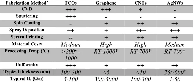
Table 1.2 provides a brief summary of some fabrication methods of electrodes using transparent conductive materials, it is by no means exhaustive, but allows a simple comparison of the currently available and emerging materials.
Table 1.2: General guide to transparent conductive material electrode fabrication methods. + symbols indicate positive results – symbols represent poor results.
♦Fabrication method refers to the production of electrodes directly not the production of
the constituent components which are used to fabricate the electrode itself.
▲Deposition temperatures of TCO’s usually require several hundred degrees Celsius or
the use of vacuum processes such as sputtering.
*Electrodes can be fabricated at RT but if device fabrication requires high temperature processes, vacuum or encapsulation are required to stabilize the films.
#Thickness is diameter and density dependant though with high pressure it can be
reduced to the diameter of a single nanowire.
Reduction of the sheet resistances of both graphene and carbon nanotubes can be achieved by doping the films but typical resistances of undoped films are shown in the table. The processing temperature indicated in Table 1.2 refers to the range of temperatures that the film may be exposed to during device fabrication. The low temperature refers to the lowest temperature that films can be fabricated at and the upper value is related to the stability of the material. Each type of TCM has strengths and weaknesses and in the end the material to use must be determined by the specific needs of the application.
For the properties mentioned in Ag nanowires are able to meet or exceed the toughest demands of existing applications. From this it can be seen that the available deposition methods for Ag nanowires are cheap and compatible with large scale samples. In light of this fact and the properties highlighted by De[6]
and Sorel[12] the remainder of this thesis will focus on the use of silver nanowire
networks as a TCM. This chapter will discuss the production of Ag nanowires and fabrication of TCMs with very promising properties produced by low-cost, solution-based, methods. Some time is also spent to discuss the application of
Fabrication Method♦ TCOs Graphene CNTs AgNWs
CVD
+++
+++
+
-
Sputtering
+++
-
-
-
Spin Coating
-
+
++
++
Spray Deposition
++
+
+++
+++
Screen Printing
--
+
++
++
Material Costs
Medium
High
High
Medium
Processing Temp (ºC)
>200
▲-1000
RT-1000*
RT-700*
RT-700*
Uniformity+++
+
++
++
Typical thickness (nm)100-300
<5
<10
25>600
# Typical Rs (Ω/□)5-100
300-5000
100-300
1-50
17
this material to devices, although several new applications have been recently demonstrated with silver nanowire networks, like EMI Shielding,[13,14] and RF
antenna[15–17] this chapter focuses on applications which will find large
improvements thanks to the three properties mentioned in Table 1.1.
1.2 Fabrication of silver nanowires
The synthesis of one-dimensional nanomaterials has grown impressively in the last two decades. In particular, the fabrication of metallic nanowires has been tackled recently for the development of transparent flexible electrodes. One of the very key criteria is the need to obtain materials from low cost solution-based processes. Among possible metallic nanostructures, silver nanowires (AgNWs) have been the most studied for several reasons. Bulk silver has the highest electrical conductivity thus it has been the focus of a lot of research.[18–20]
Moreover, synthesis of AgNWs is rather easy whereas protocols for large scale synthesis of nanowires from other metals are still under development. Several other metallic nanowires have been prepared so far and some of them show interesting properties for the fabrication of TCMs. In particular, copper,[21–24]
gold[25,26] and cupronickel[27] nanowires have demonstrated promising results. To
date, silver nanowires continue to be the most studied metallic nanowires.
Several routes have been followed experimentally to fabricate silver nanostructures with various shapes and form factors. These methods include the hydrothermal method, microwave-assisted process, electrochemical technique, UV irradiation technique, template technique… (see Coskun et al.[28] and Chen et
al.[29] and references therein). When compared to these methods, the polyol
approach appears as the most promising synthetic procedure regarding ease of mass production, cost and simplicity. This method proposes a simple route for the synthesis of metal nanoparticles through reduction of metallic salts by a polyol, generally ethylene glycol.[30,31] Crystallization of noble metals usually
leads to highly symmetric cubic unit cells. Thus, to obtain the growth of nanowires from isotropic solutions, some form of anisotropic confinement must be applied in order to achieve one-dimensional growth.[32] The polyol method of
fabrication of AgNWs was first developed by the team of Xia.[18,20] Ethylene
glycol reduces the metal precursor (usually silver nitrate) in the presence of a nucleating agent and poly-vinylpyrrolidone (PVP). The PVP plays the role of capping agent capable of controlling the growth rates of different faces of silver nanospecies. Thus the PVP is responsible for the introduction of anisotropic confinement. The near-unanimous choice of ethylene glycol as the reductant is based on its ability to solvate both AgNO3 and PVP, and its boiling point (196 °C)
which allows synthesis at high temperature.
The exact mechanism of AgNW growth is complex and as yet has not been entirely clarified. First, ethylene glycol reduces Ag+ ions in Ag atoms, thereby
inducing silver crystal formation and subsequently growth of silver nanostructures. The synthesis of AgNWs has three distinct steps; nucleation, evolution of nuclei into seeds and growth of seeds into nanocrystals. In these
18
steps the phenomena of atomic addition and aggregate formation are essentially governed by mechanisms of diffusion and surface energy minimization. By modifying the thermodynamics and kinetics of each of these steps, it is possible to have some control on the form of the synthesized nanocrystals.[33] Different
approaches have been explored. The addition of particles playing the role of seeds can change the process of nucleation. Various nucleating agents, either in a pure form or as combination of a few salts, have been used to study the effect on AgNW growth.[20,29,34–36] In general, chlorinated derivatives give good results,
and in particular NaCl is often preferred. The presence of a nucleating agent directly affects the morphology of metallic seeds during their initial formation. Thus, the addition of NaCl leads to the formation of AgCl nanocrystallites and reduces the concentration of free cationic silver ions in the solution during initial seed formation. These slow reaction conditions enable the formation of the thermodynamically more stable multiply twinned Ag seeds required for wire growth. The seed structures have an important role in the shape evolution of metal nanocrystals and therefore in the resulting materials. It has also been demonstrated that the addition of traces of salts involves selective oxidative etching controlling the structure and population of seeds once formed. Ag nanocubes or AgNWs can be obtained selectively just by modifying salt concentrations.[37–39] These parameters are key for the fabrication of
one-dimensional Ag nanostructures. According to Xia et al.,[18,33,40] the nanowires are
derived from multiple-twinned particles. Among the various possible seed structures (crystal, simple twin or multiple twins), the multiply twinned decahedra is the most thermodynamically stable seed, as it is bound almost entirely by the lower energy {111} facets. It is therefore the most naturally abundant seed but also the most reactive because of the presence of twin defects.
Figure 1.2 Schematic illustration of the mechanism proposed to account for the growth of silver nanowires with pentagonal cross sections: (A) Evolution of a nanorod from a multiply twinned nanoparticle (MTP) of silver under the confinement of five twin planes
and with the assistance of PVP. The ends of this nanorod are terminated by {111} facets, and the side surfaces are bounded by {100} facets. The strong interaction between PVP and the {100} facets is indicated with a dark-gray colour, and the weak interaction with
the {111} facets is marked by a light-blue colour. The red lines on the end surfaces represent the twin boundaries that can serve as active sites for the addition of silver atoms. The plane marked in red shows one of the five twin planes that can serve as the
internal confinement for the evolution of nanorods from MTP. (B) Schematic model illustrating the diffusion of silver atoms toward the two ends of a nanorod, with the side
surfaces completely passivated by PVP. This drawing shows a projection perpendicular to one of the five side facets of a nanorod, and the arrows represent the diffusion fluxes
19
Sun and co-workers[41] have recently reported that each nanowire is
composed of a heavily strained core encapsulated in a less-strained sheath. The crystalline defects where the cores are exposed provide active sites for growth of the nanowires along their longitudinal axes, while the less-strained side surfaces of the nanowires, bound by {100} facets, have lower reactivity towards the deposition of silver atoms (see Figure 1.2).
Once the pentagonal rod is formed, PVP plays a critical role in the growth mechanism. Originally used to prevent the aggregation of nanoparticles, it has also proven to be an agent controlling the structure of the nano-objects. Indeed, it reacts preferentially with the {100} facets of the silver nanoparticles, through interactions between surface silver atoms and the oxygen atoms of the PVP carboxyl groups.[42] Tests performed with other polymers like poly(ethyleneoxide)
(PEO) or polyvinylalcohol (PVA) did not lead to good nanowire formation.[20]
Concerning the experimental protocol of the synthesis, many parameters have to be tightly controlled, which is a common feature for the synthesis of nanoparticles. A recently published parametric study gives some details related to the effects of temperature, injection rate, molar ratio of PVP to silver, NaCl amount and stirring rate.[28] All of these parameters are important and for some
of them tiny changes can lead to dramatic alterations of the nanoparticle’s size and shape. It should also be emphasized that the quality of chemical reagents is extremely important, in particular the purity of the ethylene glycol. A few grams of AgNWs can be obtained through a single experiment which allows large area deposition considering that only few tens of mg are deposited per m² to obtain a ~90 % transparency,[43] though this is dependent on deposition technique and
wire geometry. The nanowires generally have diameters in the order of a 50-150 nm and lengths of 5-50 µm, resulting in an aspect ratio (length/diameter) typically in the 50-500 range (see Figure 1.3).
Figure 1.3 SEM images of silver nanowires at two magnifications
Recently, very long AgNWs have been synthetized thanks to a successive multistep growth method. Very high aspect ratio of 1000-3000 with lengths of over 300µm and diameter of less than 150 nm were obtained.[44] According to the
percolation behaviour of 2D stick systems as discussed in chapters 2 and 3 these nanowires represent an ideal candidate for transparent electrode fabrication.
After the synthesis, the as-obtained product requires some purification. Indeed, a mixture of nanowires and nanoparticles in organic solvent is generally
20
obtained. To remove most of the ethylene glycol and excess PVP, several washes with acetone are commonly used. To separate the nanoparticles from the nanowires the product solution is put through a centrifuge. According to different research groups, the parameters of the commonly used centrifugation procedure can be changed from 20 min at 2000 rpm[20,34,45], 6000 rpm[28] or 8000
rpm[46] to 10 min at 16000 rpm.[47] Most of the time the product is then dispersed
in another solvent such as water[17,28,46–48], ethanol[28,34] or methanol[49] to be
washed a second time. Filtration has also been described to further purify the product, either by filtering through a polycarbonate membrane with 0.8 µm pore size[35,42] or a glass filter with mean pore size of 5-40µm.[50,51] Although less
common, cross-flow filtration is also a possibility.[52] Another very
straightforward method is to let the crude reaction mixture settling for few days before removing supernatant. This decantation technique allows easy production of a high quantity of nanowires in a single run.[53]
1.3 Fabrication of silver nanowire networks
The development of high performance transparent conductive material is increasingly requiring the use of nanostructures. Therefore, it is necessary to develop simple, reliable and cost-efficient fabrication techniques to achieve both random and ordered nanowire arrays. Assembling such networks is also a critical step to control their resulting electro-optical properties. In respect to their physical properties and ease of synthesis, high aspect ratio metallic nanowires are one of the most attractive materials to fabricate such networks.[54]
Random nanowire networks can be readily and cheaply made by solution-process techniques such as spray coating[50,55–57], drop casting[58–60], spin
coating[61,62] or rod-coating.[63] All these techniques are compatible with low
temperature deposition processes (<200 °C) and do not require any vacuum equipment. In addition techniques such as spray coating are easily surface-scalable. Such solution-processed electrodes have already demonstrated their ability to be integrated into operational devices such as organic solar cells.[58,62]
Nevertheless, while working with colloidal solutions and depositing them as thin films, it is often difficult to achieve high reproducibility as determined by comparing the opto-electrical properties of different networks. It is well-known that drop cast nanowire networks may show spatial inhomogeneities known as “coffee ring effect” on the substrates during the solvent evaporation step.[63,64]
Films obtained from air-spraying coatings are usually more homogeneous and tend to form much more uniform networks.
Methods for ordering and control of nanowire arrangements have attracted increasing interest. Oxide nano templates such as anodic alumina have been used to separate and order metallic nanowires.[65,66] Polydimethylsiloxane
stamps have also been successfully used for dry transfer printing.[19,67,68] A wealth
of other different and original techniques such as blown-bubble film technique,[69]
controlled dip coating,[70,71] microfluidic assembly,[72,73] electronic/magnetic
21
assembly of nanowires,[80–82] direct gravure printing,[83] and electrospinning[23,84]
have also been attempted to produce high quality ordered nanowire arrays. One of the most important points to be addressed for device integration is the surface roughness and the contact resistance between nanowires. The former can be addressed by lamination[85] preventing shunts from occurring,[36]
embedding nanowires within a transparent polymer using a wet chemical process as demonstrated by Zeng et al.[86] or by sandwiching a metallic nanowire
network in between two ZnO layers.[87] Junction resistances can be lowered by
annealing which can be made very spatially selective using plasmonic welding.[88]
Lastly, improving thermal and more generally environmental stability is a critical issue to address for integrating nanostructures in devices. Embedding within oxide materials is proving to be a very promising way to achieve this. Indeed, it has been used to prevent thermal degradation of silver nanowire networks.[65,84,87,89,90] Ramasamy et al.[90] showed that their TiO
2 encapsulated
silver nanowires are thermally stable up to a temperature of 750 °C. However in the case of Ramasamy, the thermal annealing was performed under vacuum, in which case as we demonstrate in chapter 5 un-encapsulated wires are also stable to >700 °C.[91] Recently, Chung et al.[61] and Kim et al.[87] also demonstrated that
such embedding is also beneficial for lowering junction resistances and smoothing the surface morphology, improving the mechanical adhesion to the substrate while maintaining good mechanical flexibility.
1.4 Electrical properties
The electrical properties of nanowire networks are dependent upon several characteristics of the nanowires themselves and of course the network morphology. In general the resistance of the network increases as the length of the nanowires used decreases, this trend is continued if the wire diameter is decreased.[12,21] This increase of resistance with decreasing wire diameter is due
to an increase of the individual nanowire resistance. This phenomena was studied by Bid et al.[92] who attributed the increase in resistance to surface
scattering of the electrons, as the diameter of the nanowire reduces close to or below the mean free path of electrons in the bulk material the role of surface scattering becomes dominant. The dominance of surface scattering causes a reduction of the mean free path and causes an increase in the resistivity above that of the bulk.
The role of the nanowire length is less straightforward as the dependence is a direct result of the percolative nature of the conduction mechanism in nanowire networks. In the fabrication of nanowire networks nanowires are deposited onto a substrate layer, when two nanowires touch they form a junction connecting the two wires electrically. The formation of a conductive electrode requires many such junctions to create a conductive pathway across the electrode. Hecht et al.[93] take an elegantly simple view of the conduction mechanism to
explain the dependence of network resistance on length, although initially considered for carbon nanotube networks it is also applicable for metallic
22
networks. Put simply, the concept is that for a given network size the minimum number of nanowires required to cross it is inversely proportional to the square of the nanowires lengths. The orientations of the nanowires determine the number of junctions required to make the network percolate, but the minimum number is determined by the length of the wire. In this model the longer nanowires require fewer wires to make a conduction path across a given space, thus they have less junctions and fewer transfers between wires. This results in the lower resistances observed in networks made of long wires.
Beyond the dimensions of the wires themselves, the wire density plays a large role in the conduction properties of the network. Many studies have shown that increasing the number of wires decreases the resistance, however this also results in a decrease in the optical transmission of the network.[19,21,23,36,86] Striking
a balance between the electrical and optical properties has long been the challenge for transparent conductive materials. Among others, there are two specific advantages of nanowire networks as transparent conductive materials. One is the low sheet resistances achievable with nanowire systems which can be on the order of a few ohms per square, and the other is the transparency in the infra-red region of the spectrum. This point will be covered in more detail in section 1.5.
The overall resistance of metallic nanowire networks depends on the material used to make the network, so far mainly copper and silver networks are being studied with the silver networks having the better electrical properties. Resistance of the network is also determined by the nanowire density and the junction resistance. The diameter and length of the nanowires play a crucial role in the required density for percolation and hence the number of conduction pathways through the network. Increasing the density of nanowires above the percolation threshold results in conduction pathways through the network that are in parallel, hence as the number of conduction paths increases the resistance decreases. The junction resistance is determined by the physical properties of the junction, these are dependent on how the nanowires are grown, purified, and deposited. Modification of the junction resistance has been studied in the literature and methods such as thermal annealing[19,43,86,94] high pressure[94],
electrical annealing[43], optical sintering[88] and encapsulation[63,86] have all been
shown to reduce the resistance of the network. Some examples of post-treatments and their effects on the morphology of the network are provided in Figure 1.4. This provides a contrast in the final electrode geometry, for the thermal annealing (Figure 1.4 2b) case the junctions’ electrical properties are improved with some minor changes to the network, in the case of mechanical pressure (Figure 1.4 4b) the network morphology is reduced to the width of a single wire.
23
Figure 1.4 SEM images of silver nanowire networks, the a) series are top down views of the sample and the b) series show off angle cross-sectional views. Images 1a-b) are of as-deposited nanowire networks 2a-b) show the effect of thermally annealing at 200ºC for 20 min. 3a-b) show an as-deposited network after rinsing in water and ethanol and 4a-b)
show the effect of 5s of mechanical pressure applied at 25 MPa. Images adapted from[94] The I-V characteristics of metallic nanowires at low voltages have been shown to be close to linear[88,95] and at higher voltages the electrical breakdown
mechanism of individual single crystal nanowires has been determined to be due to electro-migration of atoms within the wires.[95] The nanowires will be subject
to Joule heating as a result of current flow. However, the electrical resistance of the individual wires is low and the thermal conductivity of the wires is high. As a consequence, the thermal energy is quickly distributed throughout the network. In this case it was shown that electro-migration will cause failure of the networks before the critical temperature (the temperature required to cause spheroidization) to cause thermal failure is reached, as shown in Figure 1.5.
Figure 1.5 Electrical breakdown of a silver nanowire, two measurements were performed (AB and CD). The images show the wire before and after breakdown. Due to
the position of the failure in each case it was determined that electro-migration is the most likely candidate as the failure mechanism. Scale bar in A) is 200 nm.[95]
24
Failure due to electro-migration is expected to occur close to junctions in the nanowire network which carry high current loads. In general electro-migration is expected to dominate the electrode failure under high current loads, the exception to this is the case where the junction resistance is high. In this case the Joule heating is localised at the junctions of nanowires in the network will act to increase the local temperature. Fortunately in this case it typically results in a reduction of the junction resistance through thermal sintering of the junction, which then reduces the heat produced at that point.
1.5 Optical properties
The use of optical properties of nanoscale particles is not really a new development, our ancestors put them in good use when fabricating magnificent colour pigments for stained glass. The vivid colours of metal colloids are a result of elastic light scattering. When an incident electromagnetic field impacts on a metallic nanoparticle, the electric field component will set into collective motion of both the bound and the free electrons with respect to fixed positive ions of the metal. This leads to electronic (which are essentially independent of the particle size) and geometric resonances over some spectral regions, effectively polarizing the material. Such polarization occurs if the particle size (the radius r of a spherical particle for example) is a multiple of the incident wavelength value. In that case, very narrow peaks are added to the extinction and scattering efficiencies. The former can be accurately described using the classical Drude-Lorentz-Sommerfeld equation for the resulting dielectric function:
(1.1)
Where j and fe are the resonant frequency and the damping constant of
the jth harmonic oscillator, respectively. fe is the damping constant of the free
electrons and ωp the bulk plasma frequency.[96]
In metals though, the contribution of free electrons is dominating the dielectric function resulting in a remarkable effect of light coupling to metallic nanoparticles via the excitation of surface-plasmon polaritons (SPPs) (as opposed to “bulk” plasmons) theorised by the pioneering work of Ritchie[97] in the 1950s.
Surface plasmons are simply plasmons confined to the surface and are directly responsible for the geometry-dependence of nanoparticle optical responses. They have both longitudinal and transverse components and can actually be observed at high spatial resolution with electron-energy loss spectroscopy experiments[98,99]
or scanning near-field optical microscopy.[100,101] SPPs stems from the relative
difference of permittivities between the metals and the surrounding non-conducting (dielectric) media. For instance, for metallic cylinders of infinite length and small diameter, the resonance condition for an SPP resonance is given by: ε1=- εM and ε2 ~ 0 where ε1 is the real part of the dielectric function of the
particle, εM the dielectric function of the surrounding medium and ε2 the
j j j j j fe p iωω ω ω ω S + iωω + ω ω = ω ε 2 2 2 2 2 125
imaginary part of the dielectric function ε.[96] Surface plasmons can be damped by
surface roughness, domain boundaries or any other sort of defects.
Having light being concentrated and channelled over the surface of nanoparticles as well as in between them results in a strong electromagnetic field enhancement. Indeed, the amplitude of the electromagnetic field observed in the vicinity of nanoparticles[102,103] can amount to several hundred times that of the
incident field in places called “hot spots”. Garnett et al. [88] put this effect to a
practical use performing plasmonic welding to assist sintering metallic nanowires into large interconnected networks. Spechler and Arnold also used this method but employed a pulsed laser to minimise the excess energy input.[104]
This feature is also used for surface-enhanced Raman spectroscopy.[65] These
phenomena also illustrate what is called dependent scattering or “optical antenna effects”. Indeed, while individual nanoparticles exhibit a single or a few plasmon resonances, much more complex resonance spectra are observed for interacting and coupled structures. Figure 1.6 shows different transmittance spectra of transparent conductors in the visible/near infra-red range.
Figure 1.6 Vis-NIR transmittance spectra (substrate subtracted) of indium tin oxide, aluminium-doped zinc oxide, PEDOT:PSS, silver nanowires and single walled carbon
nanotubes.
The plasma frequency of indium tin oxide and aluminium-doped zinc oxide falls in the near-infrared so that the transmittance drastically decreases in this region, silver nanowires and carbon nanotubes do not show such a feature and demonstrate similar transmittance in the visible range. For applications requiring conductive films that are transparent in the infra-red region of the spectrum, nanostructured films of metallic nanowires or carbon nanotubes are an excellent choice. In the case of silver nanowire networks, the transmittance loss is mainly accounted for by reflective scattering of light by the nanowires themselves.[61] In addition there is a significant reduction of the reflectance since
there is a refraction index gradient (directly resulting from having nanowires suspended in air) which is an inherent factor enabling better coupling of light to the material. [105]
26
On a final note, the ratio of diffuse transmission to direct transmission of light (the haze factor) of a material can be considered a critical factor for some applications. It is dependent on the experimental conditions and methods used for fabrication of the network. It is possible to fabricate a broad range of metallic nanowire networks with haze factors from <2% to more than 30%.[106] This range
allows metallic nanowire electrodes to be fabricated to suit many different applications.
As already briefly discussed in section 1.1 the proportion of scattered transmitted light is an important parameter which should be considered alongside optical transparency and sheet resistance. The Haze factor is associated with the degree to which transmitted light is scattered. A low Haze factor is required for display applications while higher values are desirable for enhancing the path length of light in the absorbing layer of a solar cell, thus improving the photovoltaic efficiency.[107] Haze factor is usually not considered, for instance
when calculating the figure of merit (FoM), however recent studies have focused on its importance.[106,108,109] Unfortunately it is still difficult to provide a fair
comparison and discussion on AgNWs Haze factor since literature reports very dispersed data relating to the Haze factors of nanowire networks. Actually Haze factor depends upon several parameters including NW density or diameter,[106]
deposition method and post processing. Clearly, more work should be dedicated to this topic as it is of crucial importance for the optimal integration of AgNW based transparent electrodes in real devices.
1.6 Optimising the electro-optical properties
Optimising the properties of a TCM is a delicate challenge which depends upon the application considered. Such a task is associated with the inherent trade-off between the two requirements of electrical conductivity and optical transmittance. A material transparency can be improved by decreasing the sample thickness for a thin film (such as TCO) or the density of conducting nanoparticles (such as AgNWs or CNTs or disordered arrays of exfoliated graphene flakes). However a very low thickness or low density results in an increased resistance, in percolating systems this is due to the reduced number of conduction pathways. This feature is well illustrated by Figure 1.7a where transmittance versus sheet resistance has been plotted for graphene, single wall carbon nanotubes (SWNTs), Cu and Ag NWs.[6] Such a set of data points is
associated with a series of specimen with varying thickness or density. The data can be fitted by using two different regimes which can be ascribed to bulk-like and percolation behaviour.[6] For each material considered, the bottom left
portion of the data (fitted by the solid line and corresponding to thicker films) is associated with bulk-like materials for which dc conductivity is invariant with sample thickness. Another dependency should be considered for the high transparency regime where deviation from bulk-like behaviour and can be explained by percolation effects as revealed by the good fit between the dashed lines and the data in the top right region of Figure 1.7a. A discussion of the
27
equations used to fit this data can be found in the work of De and Coleman[6]
which is also discussed in chapter 2 section 2.5. When the density of nanowires or nanotubes is decreased the sample state approaches the threshold for network percolation. At this point the probability that the network conducts is 50%; as the percolation threshold is crossed the network becomes less and less likely to contain conduction pathways and consequently the sheet resistance soars.
Figure 1.7 (a) Optical transmittance (at 550 nm) versus sheet resistance for transparent conductors composed of nanostructured materials. Each set of points can be divided into two regimes: the bulk regime (solid line) and the percolation regime (dashed line). [6]
. (b) Optical transmittance (at 550 nm) versus sheet resistance for graphene,[110–115]
carbon nanotubes,[19,56,116–121]
Ag NWs[55,57,58,68,88,94,106]
and ITO. [10,19,122]
The balance between electrical and optical properties should be quantified to allow comparison of the performance of TCMs. Therefore Figures of merit (FoM) are considered based on the pursued physical properties. A traditional FoM as defined by Haacke[123] is commonly used:[10,113]
(1.2)
Where T is the transmission measured at a wavelength of 550nm, which corresponds to the maximum human visual sensitivity and the peak in photon output of the sun. Note as well that another FoM often considered is the ratio between the electrical conductivity and the optical absorption coefficient.
Figure 1.7b exhibits experimental optical transmission and sheet resistance data associated with graphene,[110–115] carbon nanotubes,[19,56,116–121] Ag
NWs[55,57,58,68,88,94,106] and ITO. [10,19,122] The lines show iso-values of the FoM
defined by equation 1.2. The larger the FoM values are, the better are the associated electro-optical properties (so the ideal region corresponds to the top left of this graph). While a dispersion of the data points can be observed, general trends can be stated. ITO properties are still the best, while metallic nanowires exhibit rather promising properties. Carbon nanotubes are associated with lower FoM values because of the high junction resistance between carbon nanotubes. Graphene exhibits rather scattered data and except for some studies, such as
S R T FoM 10
![Figure 1.9 Flexible organic solar cell in operation (left) and the I-V curves at different angles (right) from [147]](https://thumb-eu.123doks.com/thumbv2/123doknet/6196289.159753/33.893.140.771.318.565/figure-flexible-organic-solar-operation-curves-different-angles.webp)