HAL Id: hal-02552632
https://hal.archives-ouvertes.fr/hal-02552632
Submitted on 16 Dec 2020
HAL is a multi-disciplinary open access
archive for the deposit and dissemination of
sci-entific research documents, whether they are
pub-lished or not. The documents may come from
teaching and research institutions in France or
abroad, or from public or private research centers.
L’archive ouverte pluridisciplinaire HAL, est
destinée au dépôt et à la diffusion de documents
scientifiques de niveau recherche, publiés ou non,
émanant des établissements d’enseignement et de
recherche français ou étrangers, des laboratoires
publics ou privés.
In Situ Microgravimetric Study of Ion Exchanges in the
Ternary Cu-In-S System Prepared by Atomic Layer
Deposition
Harold Le Tulzo, Nathanaelle Schneider, Frédérique Donsanti
To cite this version:
Harold Le Tulzo, Nathanaelle Schneider, Frédérique Donsanti. In Situ Microgravimetric Study of Ion
Exchanges in the Ternary Cu-In-S System Prepared by Atomic Layer Deposition. Materials, MDPI,
2020, 13 (3), pp.645. �10.3390/ma13030645�. �hal-02552632�
Materials 2020, 13, 645; doi:10.3390/ma13030645 www.mdpi.com/journal/materials
Article
In Situ Microgravimetric Study of Ion Exchanges in
the Ternary Cu-In-S System Prepared by Atomic
Layer Deposition
Harold Le Tulzo 1,2, Nathanaelle Schneider 1,3,* and Frédérique Donsanti 1,4,*
1 Institut Photovoltaïque d’Ile de France (IPVF), 18 boulevard Thomas Gobert, 91120 Palaiseau, France; harold.letulzo@gmail.com
2 French Environment and Energy Management Agency (ADEME), 20 avenue du Grésillé, 49004 Angers, France
3 CNRS, Institut Photovoltaïque d’Ile de France (IPVF), UMR 9006, 18 Boulevard Thomas Gobert, 91120 Palaiseau, France
4 EDF Research & Development, 18 Boulevard Thomas Gobert, 91120 Palaiseau, France
* Correspondence: n.schneider@chimie-paristech.fr (N.S.); frederique.donsanti@edf.fr (F.D.)
Received: 17 December 2019; Accepted: 21 January 2020; Published: 1 February 2020
Abstract: Reaction mechanisms during the growth of multinary compounds by atomic layer
deposition can be complex, especially for sulfide materials. For instance, the deposition of copper indium disulfide (CuInS2) shows a non-direct correlation between the cycle ratio, the growth per
cycle of each binary growth cycles, i.e., CuxS and In2S3, and the film composition. This evidences
side reactions that compete with the direct Atomic Layer Deposition (ALD) growth reactions and makes the deposition of large films very challenging. To develop a robust upscalable recipe, it is essential to understand the chemical surface reactions. In this study, reaction mechanisms in the Cu-In-S ternary system were investigated in-situ by using a quartz crystal microbalance system to monitor mass variations. Pure binary indium sulfide (In2S3) and copper sulfide (CuxS) thin film
depositions on Al2O3 substrate were first studied. Then, precursors were transported to react on
CuxS and In2S3 substrates. In this paper, gas-phase ion exchanges are discussed based on the
recorded mass variations. A cation exchange between the copper precursor and the In2S3 is
highlighted, and a solution to reduce it by controlling the thickness deposited for each stack of binary materials during the CuInS2 deposition is finally proposed.
Keywords: ALD; sulfide materials; thin films; QCM; CIS; exchange mechanisms
1. Introduction
Atomic Layer Deposition (ALD) is a technique based on self-limited surface chemical reactions, where the precursors are injected successively in a reactor under vacuum and heated at a relatively low temperature [1–4]. By exploiting its unique properties, conformal, pinhole-free, and precisely controlled (thickness, composition and interfaces) ultrathin binary, but also multinary films, can be synthesized. In the case of multinary compounds (ternary, quaternary materials, etc.), the most common ALD approach is the so-called “supercycle synthesis strategy” that consists of alternating binary ALD cycles [5–7]. Among its parameters, the cycle sequence (i.e., the order of the precursor doses) and the cycle ratio (i.e., the number of cycles of one binary process vs. the total number of cycles) are essential to obtain a homogeneous film. Added to these, nucleation delays, exchange mechanisms, growth rate, and temperature window differences complicate the deposition of such multinary compounds and make the control of the process parameters crucial [5–7].
The sulfide class contains a wide range of materials in which syntheses by ALD have been relatively less explored compared to others, such as oxide and elementary metals. Their interests are
particularly driven by the energy-related fields [8]. In particular, Copper Indium Disulfide (CuInS2,
CIS) is a suitable material to be used as a thin absorber in photovoltaic devices (direct bandgap ≈ 1.5 eV, absorption coefficient > 104 cm−1 for λ = 500 nm) [9,10], and CIS-type solar cells with homo- [11]
or hetero- [12,13] junction architecture have been reported. CIS synthesis has been reported by various routes, such as thermal evaporation [11], co-evaporation [14], sputtering [15], electrodeposition [16], spray pyrolysis [17], spray ion layer gas reaction (spray-ILGAR) [18], atmospheric pressure spray chemical vapor deposition (APCVD) [19], and ALD [20,21]. The complexity of the ALD deposition process of CIS, as for sulfide multinary compounds in general, lies in the high propensity of the cation exchange mechanisms, the greater diffusion rates and the unintentional annealing of the labile sulfur [8,21–23]. Besides a deep understanding and control of the chemical process, a rigorous cleaning of the various parts of the reactor must often also be carried out to obtain a homogeneous film [21,24]. To date, two teams have mastered these conditions and reported CIS homogenous deposition by employing quartz and small scale (5 × 5 cm²) reactors [20,21,25].
In the present work, an upscale was attempted to deposit CIS in a larger reaction chamber (15 × 15 cm²) using the supercycle strategy of Schneider, et al. [17]. A non-homogeneous film composed of copper sulfide (CuxS) upstream, indium sulfide (In2S3) downstream, and a CuxInyS2 film in the middle
of the reaction chamber was obtained. The CuxInyS2 film area was inversely proportional to Cu and
In concentrations in the flux direction from the inlet to the outlet. Variation of process parameters, such as the cycle ratio, the reactor temperature, or the Cu precursor pulse time, showed a shift in the position of the CuxInyS2 film area but failed to widen it. Thus, to tailor a working process on a large
scale, understanding of the surface chemical reactions was essential. To investigate and control those phenomena, mechanism studies using a quartz crystal microbalance (QCM) system was performed to monitor thickness and mass variations. First, pure films of In2S3 and CuxS were grown on Al2O3.
While In2S3 had already been investigated with by in-situ QCM [26–28], the growth of ALD-CuxS was
investigated, to the best of our knowledge, for the first time with this set of precursors. Then, ion exchanges in the Cu-In-S ternary system were investigated by monitoring the growth of In2S3 on CuxS
and of CuxS on In2S3 but also the behavior of the Cu precursor on In2S3. These have evidenced
additional reaction paths that need to be controlled to pursue large scale CIS synthesis.
2. Materials and Methods
2.1. Thin Film Synthesis and In-Situ Growth Characterization
2.1.1. Atomic Layer Deposition
In2S3 and CuxS thin films were grown in a Beneq TFS-200 ALD reactor (15 × 15 cm²; Beneq Oy, Espoo,
Finland), at Tdep = 180 °C for In2S3 and Tdep = 160 °C for CuxS, respectively. High purity nitrogen
99.9999% (N2, Air Liquide, Paris, France) was used as carrier and purge gas. The carrier gas flow rate
was set at 600 sccm. In the reaction chamber, the pressure was kept around 1 mbar. Indium(III) acetylacetonate (In(acac)3, 98%, Strem Chemicals, Bischheim, France), copper(II) acetylacetonate
(Cu(acac)2, 98 + %, Strem Chemicals, Bischheim, France), and H2S (99.5%, Air Liquide, Paris, France)
were used as In, Cu, and S sources, respectively. All chemicals were used as received, without further purification. A mass of 2 g of In(acac)3 and Cu(acac)2 was heated in two different hot solid sources
(system Beneq HS300, Beneq Oy, Espoo, Finland) at TIn(acac)3 = 150 °C and TCu(acac)2 = 140 °C. To ensure
proper mass transport of the metal precursors, “booster” and “combination” modes were chosen. In “booster” mode, N2 carrier gas is injected in the precursor source before its pulse. “Combined” mode
is composed of five steps ([t1/t2/t3/t4/t5]). N2 is first injected in the source (t1, as in “booster” mode), all
valves are kept closed (t2), precursor is pulsed (t3), and N2 is injected during the last part (t4) and after
(t5) the precursor pulse. Typical growth cycles are {In2S3} = {[In(acac)3]/N2/H2S/N2 = [0.5/0.5]/5/0.5/5 s},
and {CuxS} = {[Cu(acac)2]/N2/H2S/N2 = [0.5/0.2/0.5/10/0.5]/5/0.5/5 s}. A 10–50 nm thick Al2O3
passivation film was deposited on the reaction walls, prior to each experiment, and on the quartz crystal. It mitigates the cation exchange mechanisms [24,29], so that only the reactions between the
quartz surface and the precursor(s) pulsed are revealed. Each experiment is referred in the text by the names given in the Table 1.
Table 1. In situ microgravimetric experiments between precursors Cu(acac)2-In(acac)3-H2S and the sulfide materials In2S3 and CuxS initially deposited on the quartz crystal microbalance (QCM).
Experiment Substrate (Estimated Thickness) PRECURSOR(s) Pulsed Sequentially TREACTOR
#1 Al2O3 (100 Å ) In(acac)3/H2S 180 °C #2 Al2O3 (500 Å ) Cu(acac)2/H2S 160 °C #3 CuxS (95 Å ) In(acac)3/H2S 180 °C #4 In2S3 (23 Å ) Cu(acac)2/H2S 160 °C #5 In2S3 (50 Å ) Cu(acac)2/H2S 160 °C #6 In2S3 (250 Å ) Cu(acac)2/H2S 160 °C #7 In2S3 (22 Å ) Cu(acac)2 160 °C #8 In2S3 (250 Å ) Cu(acac)2 160 °C
2.1.2. In-Situ Quartz Crystal Microbalance (QCM) Measurements
In-situ QCM measurements were acquired with a Colnatec Eon-LT monitor system (Greenville, United States of America), using a HT quartz crystal covered by an alloy (6 MHz initial oscillation frequency, Neyco, Vanves, France) located downstream on the cover lid of the reactor. Signal was recorded every 0.2 s and the mass resolution set in order to have the lowest thickness step precision of 0.04 Å . Measurements were done after a long enough stabilization time to reach a uniform and constant temperature in the whole reaction chamber (ΔT ± 1.5 °C). Mass variations were calculated from the thickness values by considering the average density of the films grown by ALD as determined by X-ray Reflectivity (XRR) (4.75 g/cm3 for ALD-In2S3 and 5.52 g/cm3 for ALD-CuxS).
Impedance acoustic values were set at 0.27 (calculated from the shear modulus for a spray pyrolysis-In2S3 film obtained in the literature [30]) and 0.82 (considering the covellite phase), respectively. 2.2. Thin Film Characterization
Film thicknesses and densities were determined from samples deposited on glass substrates by X-ray Reflectivity using a PANalytical Empyrean equipment (PANanalytical, Orsay, France), equipped with a PIXcel 3D detector and Cu anode providing Cu-Kα radiations. Fitting of the experimental curves were performed with X’Pert Reflectivity Software (PANanalytical, Orsay, France). The morphology of the In2S3 samples was investigated with a field-emission scanning
electron microscope (FESEM, Merlin VP Compact, ZEISS, Marly-Le-Roi, France). The electron beam acceleration voltage was set at 15 kV.
3. Results and Discussion
3.1. In-Situ Microgravimetric Study of In2S3 Material (Experiment #1)
Growth mechanism of In2S3 film was first studied and compared with the literature [26–28,31–
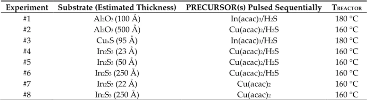
33]. Figure 1a depicts the mass variation of In2S3 deposited on an Al2O3 substrate, monitored by the
QCM during 900 cycles. The growth is non-linear as the estimated Growth Per Cycle (GPC) increases progressively until it reaches a constant value approximately equals to 0.32 ± 0.03 Å /cycle (determined by linear regression). This value is similar to what Genevée [31] (0.26 Å /cycle), Sterner [32] (0.30 Å /cycle), and Bugot [33] (0.24 Å /cycle) found using the same deposition temperature. The 400 first cycles, including the nucleation step, are characterized by a lower GPC, meaning that Al2O3
substrate partly inhibits the growth of In2S3,as observed by Sarkar et al. [27].
Figure 1b shows the mass evolution during a regular growth cycle of In2S3, i.e., of In2S3 on itself,
averaged over 10 cycles. It is characterized by a mass gain during the In(acac)3 pulse (+(43 ± 2)
ng.cm−2), a progressive mass loss during the purge (−(9 ± 1) ng.cm−2), and a mass loss during the H2S
explained elsewhere [27,28]. This description will serve as a reference for the study of ion exchanges with an ultrathin film of CuxS.
(a) (b)
Figure 1. Mass variations during the deposition of In2S3 on a QCM covered by a 10 nm-thick Al2O3 layer; (a) mass variations all along the 900 cycles; (b) mass variations during one cycle averaged over ten cycles positioned in the linear portion of the curve (a). Vertical dash lines are a help for the eye to visualize the precursor pulse times.
3.2. In Situ Microgravimetric Study of CuxS Material (Experiment #2)
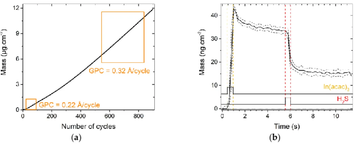
The growth mechanism of the second binary material in the Cu-In-S ternary system, i.e., CuxS,
was then investigated. The mass variation over 200 {CuxS} deposition cycles is displayed in Figure
2a. The curve and thus the growth are non-linear, as the estimated GPC varies between low (0.1 Å /cycle) and relatively high values (0.60 Å /cycle). These variations all along the deposition may be partly explained by an instability of the flux, which has been observed during preliminary optimization efforts on Cu(acac)2 transport.
Figure 2b presents the mass evolution during one growth cycle of CuxS on itself, averaged over
10 cycles (190th to 199th cycle). Estimated GPC equals 0.54 ± 0.03 Å /cycle. The mass slowly increases all along the pulse of Cu(acac)2 (+ 33 ng.cm−2 corresponding to + 0.6 Å for 10.5 s). The H2S pulse leads
to a mass gain followed by a loss of similar value. Thus, this local variation has only a very small effect on the film mass gain.
(a) (b)
Figure 2. Growth mechanisms of CuxS on a 50 nm-thick Al2O3 substrate; (a) mass variations all along the 200 cycles; (b) mass variations during one cycle averaged over ten cycles positioned in the last linear portion of the curve (rectangle number 3). Vertical dash lines are a help for the eye to visualize the precursor pulse times.
Based on the theoretical surface chemical reactions that can be predicted and the mass (or thickness) variations obtained during the experimental reaction, it is possible to estimate which CuxS
ALD with the precursors Cu(acac)2 and H2S may present a multiphasic state, that complicates the
determination of the reactions enabling its synthesis.
Ideal reaction equations and mechanisms of the stoichiometric phases CuS (covellite) and Cu2S
(chalcocite or digenite) can be hypothesized. For CuS, the overall reaction would be:
Cu(acac)2 (g) + H2S(g) → CuS (ads) + 2 Hacac (g), (1)
which can be decomposed in two half-reactions during each Cu(acac)2 and H2S pulses (with “‖-“
depicting a surface group):
|| − SH + Cu(acac)2 (g) → || − S − Cu(acac) + Hacac (g), (2) || − S − Cu(acac) + H2S (g) → || − S − Cu − SH + Hacac (g). (3) The ratio of the reaction (Rs) can then be calculated as follows:
Rs =
M(CuS)
M(Cu(acac)2)−M(Hacac)= 0.59. (4)
For Cu2S, even though the ALD synthesis of this material has been reported by several groups
[24,35–37], the detailed mechanisms is complex and, as far as we know, has never been investigated by QCM. The overall reaction may be:
2 Cu
(
acac)
2(
g)
+ 2 H2S(
g)
→ Cu2S(
ads)
+ 4 Hacac(
g)
+ S (g). (5) It is based on the assumption of the reduction of copper, from Cu2+ to Cu+, leading to a Cu-richphase (chalcocite or digenite) from a Cu-poor phase (covellite) [34], accompanied with the oxidation and subsequent evaporation of sulfur:
|| − (2 − x)[CuS] → || − Cu2−xS + (1 − x)S (s) → || − Cu2−xS + (1 − x)S (g). (6) Though this equation is slightly endothermic (ΔG = 17 kJ/mol at 100 °C for x = 0 [38]), it is driven by the non-reversible evaporation of sulfur. The ratio of the reaction (Rs) can be calculated as follows:
Rs =
M(Cu2S)
2M(Cu(acac)2)−k×M(Hacac)−M(S)
= 159.1
523−k×100−32.1, (7)
with k corresponding to the number of ligands desorbed during the Cu(acac)2 pulse, k = [0; 4]. As a
function of k, Rs differs (see Table 2).
Table 2. Theoretical ratios (Rs) of the overall reaction for the formation of Cu2S, as a function of k, the number of ligand desorbed during each Cu(acac)2 pulse.
k 0 1 2 3 4 Rs 0.32 0.41 0.55 0.83 1.75
The reaction mechanisms and the phase formations can be discussed in light of the experimental results. According to the theoretical growth mechanisms estimated for the CuS formation, the desorption of ligands during the H2S pulse step should be characterized by a thickness drop (as
M(acac) > M(SH)), which is not monitored by the QCM. The small variation during this H2S pulse
may rather be characteristic of the formation of a Cu-rich phase. Indeed, a ratio of reaction of Cu2S
close to 1, corresponding to an absence of thickness variation, can be determined for a certain value of k. We can estimate at 3.29 the number of ligands desorbed during the Cu(acac)2 pulse, while 0.71
ligands would be desorbed during the H2S pulse.
The growth mechanisms of CuxS deposited on Al2O3 monitored by the QCM seem to be
characteristic of a Cu-rich phase formation. They will serve as a reference for the microgravimetric study on the Cu-In-S ternary system.
3.3. Growth of CuInS2 Films (Experiments #3–5)
As described earlier, CIS thin film can be deposited by ALD by alternating cycles of In2S3 [26]
β-diketonates precursors and H2S, at a temperature as low as 150 °C [16]. CIS stoichiometry was
obtained only from some cycle ratios (n2:n1 > 5 at 150 °C), which demonstrated that there is a
non-direct correlation between the cycle ratio and the film composition and evidenced side reactions that may compete with ALD traditional surface reactions. Indeed, as for other copper-containing sulfide materials [24,39,40], cation exchanges promoted by a rapid diffusion may occur during the CIS synthesis. This complexity has prevented a straightforward upscale of the CIS deposition in a large reaction chamber. To evidence cation exchanges in the Cu-In-S system and identify new paths to allow the deposition of large CIS films, growth of CuxS and In2S3 on the other binary sulfide was
investigated.
3.3.1. Reaction Mechanisms of In2S3 on a CuxS Substrate (Experiment #3)
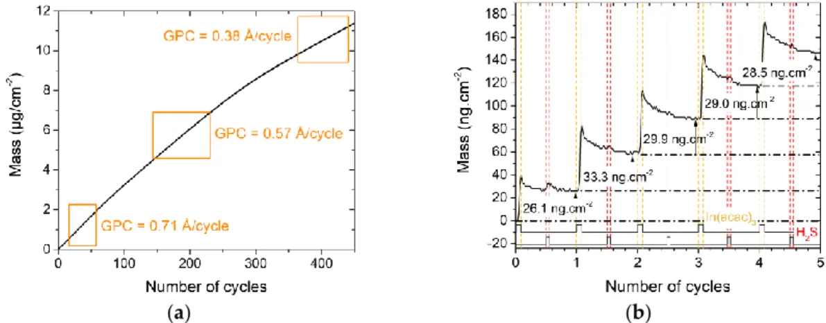
Figure 3a shows the mass variation of an In2S3 film grown on a CuxS substrate. It increases all
along the 450 cycles, but the gain progressively slows down, with estimated GPC values from 0.71 Å /cycle for the first cycles to 0.38 Å /cycle for the last cycles (averaged values). It is characteristic of a substrate-enhanced growth that occurs over a large thickness. During the last cycles, after 20 nm is deposited, the GPC (0.38 Å /cycle) gets closer to the regular GPC of In2S3 (0.32 Å /cycle).
The first cycles were studied, in particular, as ion exchanges are more likely to occur during them. Thus, Figure 3b depicts the five first cycles of the growth and evidences the mass variation during each pulse and purge. The first In(acac)3 pulse leads to a lower mass gain than the following
pulses, meaning that the surface of the substrate is less reactive or has a poorer density of absorption sites than the surface of the growing film. The H2S pulse is notably characterized by the absence or a
weak mass variation during these first cycles, while a clear drop can be seen during the H2S pulse
when In2S3 grows on Al2O3 (see Figure 1b). Two reasons might explain this behavior. First, the surface
reaction of H2S gas may be inhibited by the substrate or the In(acac)x-terminated surface fragments.
Second, the conversion from a Cu-rich phase to Cu-poor phase or covellite phase by copper dismutation may occur and some of the released sulfur remain at the surface to react with In(acac)3
(hence reducing the following mass gain during H2S pulse). No significant mass (or thickness) change
has been observed during one of the precursor pulse, such as when diethyl zinc reacts on Cu2S [24],
or when bis(N,N-disec-butylacetamidinato)dicopper(I) (CuAMD) reacts on Sb2S3 [40]. Therefore,
there is no evidence that indium does readily ion exchange with copper in a CuxS film at a deposition
temperature of 180 °C.
(a) (b)
Figure 3. Mass variations during the deposition of In2S3 on a QCM covered by CuxS (a) all along the 450 cycles; (b) zoom on the five first cycles.
To better understand the growth mechanism changes all along the deposition, first and last cycles are compared (Figure 4). Mass Gain Per Cycle (MGPC) is evidenced to vary and depends especially on the mass variation during the pulse and purge of H2S. Indeed, desorption during the
H2S pulse steadily increases when the film grows, so that the MGPC decreases. As a consequence, the
(see Figure 1b), which confirms that approximately 20 nm are necessary for the film not to be influenced by the substrate.
Figure 4. Aspect evolution of five successive cycles In(acac)3/N2/H2S/N2 distributed over the entire duration of the deposition, when the film grows on a CuxS substrate.
3.3.2. Reaction Mechanisms of CuxS on a In2S3 Substrate (Experiments #4–#6)
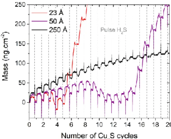
The reaction mechanisms occurring at the surface of a In2S3 substrate exposed to Cu(acac)2 and
H2S pulses have been studied. Figure 5 shows the mass variations observed on In2S3 substrates of
different thicknesses during the first cycles of CuxS deposition. The curves are not superposed, which
indicates that the exchange mechanisms differ as a function of the In2S3 thickness. For the thinner
In2S3 substrates, the curves have non uniform variations and the mass decreases to a value lower than
the initial one after several CuxS cycles, then the film grows faster. Indeed, on 23 and 50 Å -thick In2S3
substrates, while most of Cu(acac)2 pulses show a mass gain, some depict large mass losses,
respectively, the 4th and from the 10th to the 12th pulses. When the In2S3 substrate is thicker (250 Å ),
the curves have uniform variations.
Figure 5. Mass variations measured for three films of In2S3 exposed to successive pulses of Cu(acac)2 and H2S. The apparent short-time mass changes observed during the H2S pulses (estimated thickness of In2S3 = 50 and 250 Å ) are probably induced by temperature variation [41] and are considered as artefacts.
Desorption phenomena have been described for multinary sulfide materials and are often linked to high cation mobility [8,42], coupled with fast diffusion of the cations as in ZnInxSy [28]or
Cu(Zn,Sn)S2 (CZTS) [39]. Therefore, the large mass losses may be due to a gas-phase ion exchange
between the Cu and In cations, from the precursor and the film, respectively. Heavy desorbed molecules (In(acac)3) would be replaced by lighter adsorbed molecules (Cu(acac)2), through an
exchange mechanism that has to be determined. According to the shape of the curves in Figure 5, this process seems to slow down when the In2S3 film becomes thicker. As the mass loss does not occur
during the first pulse, the reaction is not instantaneous but requires several cycles to be activated. In addition, unlike when CuxS is grown on Al2O3 (Figure 2b), a mass drop occurs during most of the H2S
pulses when CuxS is grown on In2S3: first cycles for 23 or 50 Å -thick In2S3 and all along the cycles
shown in Figure 5. After the mass loss, the shape of the cycle is modified because the mass variation during the H2S pulse vanishes. This mass drop occurring during the H2S pulse may be a consequence
of the exchange mechanism as In(acac)3 molecules might be removed from the substrate as described
by the reaction drawn in Figure 6. This hypothesis can be verified by considering the sign of the mass variations with the theoretical ones of Figure 6, i.e., 4 × 𝑀(𝐶𝑢(𝑎𝑐𝑎𝑐)2) − 2 × 𝑀(𝐼𝑛(𝑎𝑐𝑎𝑐)3) > 0 during Cu(acac)2 pulse, 3 × M(H2S) − 2 × M(Hacac) < 0 during H2S pulse, and 4 × M(Cu(acac)2) − 3 ×
M(Hacac) − 2 × M(In(acac)3) > 0 for the global reaction. The recorded values: positive during the Cu(acac)2 pulse, negative during the H2S pulse and positive for the global reaction, verify the
likeliness of the hypothesis. Further evidence would require more sophisticated experiment setup, possibly with gas phase species or in-situ surface composition characterization capabilities.
Figure 6. Exchange mechanism that would explain the mass loss during a H2S pulse.
3.3.3. Reaction Mechanisms of Cu(acac)2 on a In2S3 Substrate (Experiments #7 and #8)
The aim of these experiments was to determine if the Cu(acac)2 alone can activate the cationic
exchange mechanism with the In atoms in the substrate. Compared to the {CuxS} program, the H2S
pulse is replaced by a purge, leading to the program [Cu(acac)2]/N2 = [0.5/0.2/0.5/10/0.5]/10.5 s. Figure 7a
presents the complex variations of the mass during fifty successive pulses of Cu(acac)2 on a 22 Å –
thick In2S3 film, with a zoom on the first 18 cycles in Figure 7b. A mass increase occurs during the first
Cu(acac)2 pulse (+21.2 ng.cm−2), that may be ascribed to a surface adsorption of Cu(acac)x groups on
In2S3 substrate (phase I, described by the reaction in Figure 8a). During the three following cycles
(phase II), the mass progressively decreases, especially during the purge time. Then (phase III, cycle 4 and 5), a mass loss is clearly visible during the pulse of Cu(acac)2 as it suddenly drops (down to −24
ng.cm−2). Finally, (phase IV), a mass gain is observed while Cu(acac)2 is pulsed, and this gain is
progressively reduced during the following pulses, whereas a mass loss during the purges appears.
Figure 7. Growth mechanisms when Cu(acac)2 is successively pulsed on a 22 Å -thick In2S3 film, (a) mass variations during fifty successive pulses; (b) zoom on the first 18 pulses. The roman numbers correspond to the various growth phases.
As described earlier, a desorption of In(acac)3 via an exchange mechanism is highly probable
during phase III, as presented in Figure 8c, as it leads to a mass loss (3 × M(Cu(acac)2) − 2 × M(In(acac)3)
< 0). Diffusion of Cu atoms along with a desorption of a small amount of In(acac)3 may explain the
behavior during phase II (Figure 8b).
(a)
(b)
(c)
Figure 8. (a) Surface adsorption of Cu(acac)x groups; (b) interdiffusion; (c) gas phase cation exchange mechanism.
It is possible to determine if the In2S3 substrate is totally etched. The initial mass of the In2S3
substrate being 1040 ng.cm−2 for 22 Å corresponds to a mass of 733 ng.cm−2 of In (m(In) = m(In2S3) ×
2M(In)/M(In2S3)), assuming no contaminants in the structure lattice. According to the Figure 8c
process, as three Cu atoms replace two In atoms, a Cu mass equals to 647 ng.cm−2 would be necessary
to replaceall the In in the 22 Å -thick substrate (m(Cu) = [1.5 × m(In) × M(Cu)]/M(In)). This would be characterized by a mass loss equals to 125 ng.cm−2 while the experimental mass loss is 24 ng.cm−2 (end
of phase III). It corresponds to only 19% of the mass loss estimated if all the In from the substrate was etched. Thus, it can be estimated than only 4.2 Å over the 22 Å (19%) are impacted by the cation exchange mechanism during the six first cycles of the experiment. In general, the surface saturation is improved by successive pulses of a precursor. For instance, Muneshwar and Cadien [43] have showed that in the case of ZrN and HfO2 depositions, using precursors with a high steric hindrance
(Zr(NMe2)4 and Hf(NMe2)4), GPC was increased, respectively, ~46% and ~49% by reproducing at least
3 and 6 successive pulses. However, even when considering a similar steric hindrance for Cu(acac)2,
it is surprising in our case to observe such a large mass increase (≈243%) over as much as 43 successive pulses. Hence, this confirms that additional phenomena, such as Cu diffusion, In substitution, and In desorption, occur until the 50th Cu(acac)2 pulse. The desorption of In, in particular, can explain the
mass loss during the purges and liberates S atoms, newly available to bond with the adsorbed copper molecules.
To investigate the impact of the thickness on the growth, the same experiment has been conducted on a 250 Å -thick In2S3 substrate (experiment #8), and both are plotted in Figure 9. It shows
that no mass loss is observed in the case of 250-Å thick substrate. This evidences that the growth and exchange mechanisms differ as a function of the In2S3 thickness, as represented Figure 10. This at first
surprising observation can be explained by the impact of the In2S3 film morphology. Indeed, the
morphology of the surface (Figure 11) and the crystalline character (as determined by XRD under grazing incidence, not shown here) of the film has been demonstrated to be dependent of the thickness. For the 15 nm-thick film, a Volmer-Weber growth mechanism can be considered to explain the island covered looking surface. For the thicker film, grains seem to cover the entire surface. Hence, it is possible that the cation exchange mechanism between Cu and In occurs preferentially on In2S3
islands that may have more reactive surface sites energetically favorable (Figures 5 and 9).
Figure 9. Mass variations recorded during six successive pulses of Cu(acac)2 on 22 Å - and 250 Å - thick In2S3.
Figure 10. Possible reaction mechanisms between the Cu(acac)2 precursor in a gaseous state and a In2S3 film. When ultrathin (e1), In2S3 is more affected by ionic gas phase exchange and interdiffusion phenomena compared to a thicker film (e2).
(a) (b)
Figure 11. SEM images of In2S3 films tilted at 30°, (a) 15-nm thick; (b) 35-nm thick. Process program: In(acac)3/N2/H2S/N2: [0.5/0.5]/14/0.5/2.5 s; Treactor = 180 °C.
Finally, the reaction of Cu(acac)2 alone or Cu(acac)2/H2S on a 23-Å thick In2S3 substrate are
compared in Figure 12. The slopes of the mass loss during the Cu(acac)2 pulse and of the large mass
gain that follows are similar whether H2S is used or not (see dashed lines on Figure 12). It suggests
similar desorption and adsorption rates. The minimal mass values reached are also similar (−24 ng.cm−2 for Cu(acac)2, −18 ng.cm−2 for Cu(acac)2/H2S). In the latter case, about 14% of the In contained
in the film is impacted by the exchange mechanism (3.2 Å over the 23 Å , for an initial mass = 1107 ng.cm−2) versus 19% for Cu(acac)2 alone. This difference can be explained by an enrichment of the
film in sulfur, while H2S is pulsed, characterized by a mass loss and could be written as follows, with
|| representing a surface group:
|| − Cu(acac)x+ H2S (g) → || − Cu(acac)x−1(SH) + Hacac (g). (8) The desorption of acetylacetone during the first cycles would deprive the indium in the film of acac ligands and thus reduce the desorption of In(acac)3 during the fourth cycle. The H2S pulse seems
to accelerate the cation exchange mechanism. Indeed, the mass loss phenomenon that occurs during a pulse of Cu(acac)2 happens two cycles earlier when H2S is used.
Figure 12. Mass variations observed during the first cycles of the reaction when a 22–23 Å - thick
substrate is exposed to pulses of Cu(acac)2 alone or alternated pulses of Cu(acac)2 and H2S. The dashed lines represent the slopes of the curves.
The nucleation behavior and especially the consequence of the first Cu(acac)2 exposure seems
also to differ. To estimate the coverage of Cu(acac)2 species, the number of In2S3 surface sites can be
approximated by using the In2S3 average density (4.75 g/cm3 as determined by XRR, equivalent to ρ
= 8.8 × 10²¹ “In2S3 units”/cm3), and assuming a square lattice, leading to ρ2/3 = 4.3 × 10¹⁴ “In2S3
units”/cm2.
The coverage of Cu(acac)2 can then be approximated based on the mass gain during the first
exposure. In the case of the experiment using only Cu(acac)2 precursor, 21.2 ng/cm² is deposited that
corresponds to 4.88 × 10¹³ “Cu(acac)2 molecules”/cm². The normalized coverage of Cu(acac)2 species
relative to “In2S3 units” on the surface is [4.88 × 10¹³ “Cu(acac)2 molecules”/cm²]/[4.3 × 1014 “In2S3
units”/cm2] = 0.11 “Cu(acac)2 molecules”/“In2S3 units”, i.e., a coverage of 11%. In the case of alternated
Cu(acac)2 and H2S precursor, a mass gain of 12.9 g/cm² is obtained, that yields a coverage of 7%, based
on similar assumptions. These coverage values are reasonable, as they are significantly smaller than the maximum coverage calculated to be 180% ([7.76 × 10¹⁴ “Cu(acac)2 molecules”/cm²]/[4.3 × 1014 “In2S3
units”/cm2]) according to the steric hindrance of the Cu(acac)2 molecules (see Appendix A). As the
same Cu(acac)2 pulse time is used, the coverage is indeed similar, and the observed small variations
may be due to slightly different In2S3 initial surface state.
4. Conclusions
This study is a deep investigation of the reaction mechanism and ion exchanges occurring in the ternary Cu-In-S system prepared by ALD from metal acetylacetonate precursors and H2S. This was
binary compounds on a Al2O3 substrate were first studied. It strengthened the postulated mechanism
for the ALD-CuxS formation via reduction of Cu, oxidation and subsequent evaporation of elemental
sulfur. Then, mass variations were monitored during the synthesis of In2S3 on a CuxS substrate, of
CuxS on a In2S3 substrate, and pulsing Cu(acac)2 on a In2S3 substrate. Mass variations have evidenced
gas-phase ion exchanges when Cu(acac)2 reacts on an In2S3 substrate while In2S3 growth is enhanced
by a CuxS substrate. It was particularly highlighted by a large mass loss that occurs during one or
two of the first Cu(acac)2 pulses. It has also been noted that it may be possible to reduce the cation
exchange by controlling precisely the In2S3 thickness. Indeed, from a certain thickness value (and
morphology), the reaction of Cu(acac)2 on a In2S3 substrate is even hindered, as in our case from 250 Å .
Indeed, the crystalline character of In2S3 is enhanced by the thickness, and it was shown to be more
stable when Cu(acac)2 reacts on its fully covered surface rather on growth islands. To go further,
analytical tools, such as XPS (ex-situ or in-depth) or in-situ XRF, may be employed in order to determine precisely how deep the In2S3 film is impacted by the exchange mechanism (in-depth In and
Cu concentration) as a function of the number of cycles of CuxS. In addition, Quadrupole Mass
Spectrometry measurements could help to identify the reaction by–products.
Finally, beyond the fundamental interest in understanding the ever-challenging growth of ALD multinary compounds, it also aims at allowing the upscale of an ALD recipe. Indeed, it explains why the film synthesized during the CIS deposition in the Beneq TFS-200 is not homogeneous and does not contain any indium upstream, next to the gas inlet.
Based on these observations, a nanolaminate strategy that controls finely the In2S3 thickness
deposited between each CuxS cycle, should rather be chosen to deposit homogeneous CISfilm on
large area. Another solution would be to substitute one of the metal precursor by a precursor without acac ligands as this may lead to different dynamics.
Author Contributions: Conceptualization, H.L.T., N.S. and F.D.; methodology, H.L.T., N.S., and F.D.; validation,
H.L.T., N.S., and F.D.; formal analysis, H.L.T., N.S., and F.D.; investigation, H.L.T.; resources, H.L.T., N.S., and F.D.; data curation, H.L.T., N.S., and F.D.; Writing—Original draft preparation, H.L.T.; Writing—Review and Editing, N.S., and F.D.; visualization, N.S., and F.D.; supervision, N.S., and F.D.; project administration, F.D.; funding acquisition, N.S., and F.D.
Funding: This research was supported by the French Environment and Energy Management Agency (ADEME)
via a Ph.D. grant to H. Le Tulzo and EDF and partly carried out in the framework of a project of IPVF, which has been supported by the French Government in the frame of the program of investment for the future (Programme d’Investissement d’Avenir ANR-IEED-002-01).
Acknowledgments: The authors would like to thank Daniel Lincot, CNRS for general guidance and fruitful
discussions.
Conflicts of Interest: The authors declare no conflict of interest. The funders had no role in the design of the
study; in the collection, analyses, or interpretation of data; in the writing of the manuscript, or in the decision to publish the results.
Appendix A
According to its crystal structure, the area of a Cu(acac)2 molecule can be estimated to be similar
to a rectangle, with a length of 11.1 Å (distance between C(4A) and C(5)) and a width of 4.05 Å (distance between C(4) and C(5)) [44]. Thus, the calculated area would be 44.7 Å ². When adsorbed, the complex loses a ligand and it binds through the Cu atom with a molecular axis being perpendicular to the surface as reported by Hu et al. for an adsorption on Ta(110) surface [45]. Its projection on the In2S3 surface can be modelled as a circle with a diameter of 4.05 Å , representing a
surface area of 12.9 Å ². The maximum areal density of the adsorbed Cu(acac)2 molecules would then
be equal to 7.76.1014 Cu(acac)2/cm².
References
1. Miikkulainen, V.; Leskelä, M.; Ritala, M.; Puurunen, R.L. Crystallinity of inorganic films grown by atomic layer deposition: Overview and general trends. J. Appl. Phys. 2013, 113, 021301.
2. Puurunen, R.L. A Short History of Atomic Layer Deposition: Tuomo Suntola’s Atomic Layer Epitaxy: A Short History of Atomic Layer. Chem. Vap. Depos. 2014, 20, 332–344.
3. George, S.M. Atomic Layer Deposition: An Overview. Chem. Rev. 2010, 110, 111–131.
4. Bui, H.V.; Grillo, F.; Ommen, J.R. van Atomic and molecular layer deposition: off the beaten track. Chem.
Commun. 2016, 53, 45–71.
5. Mackus, A.J.M.; Schneider, J.R.; MacIsaac, C.; Baker, J.G.; Bent, S.F. Synthesis of Doped, Ternary, and Quaternary Materials by Atomic Layer Deposition: A Review. Chem. Mater. 2019, 31, 1142–1183.
6. McDaniel, M.D.; Ngo, T.Q.; Hu, S.; Posadas, A.; Demkov, A.A.; Ekerdt, J.G. Atomic layer deposition of perovskite oxides and their epitaxial integration with Si, Ge, and other semiconductors. Appl. Phys. Rev.
2015, 2, 041301.
7. Sønsteby, H.H.; Fjellvåg, H.; Nilsen, O. Functional Perovskites by Atomic Layer Deposition – An Overview.
Adv. Mater. Interfaces 2017, 4, 1600903.
8. Dasgupta, N.P.; Meng, X.; Elam, J.W.; Martinson, A.B.F. Atomic Layer Deposition of Metal Sulfide Materials. Acc. Chem. Res. 2015, 48, 341–348.
9. Tell, B.; Shay, J.L.; Kasper, H.M. Electrical properties, optical properties, and band structure of CuGaS2 and CuInS2. Phys. Rev. B 1971, 4, 2463.
10. Neumann, H.; Hörig, W.; Savelev, V.; Lagzdonis, J.; Schumann, B.; Kühn, G. The optical properties of CuInS2 thin films. Thin Solid Films 1981, 79, 167–171.
11. Kazmerski, L.L.; Sanborn, G.A. CuInS2 thin-film homojunction solar cells. J. Appl. Phys. 1977, 48, 3178–3180. 12. Siemer, K.; Klaer, J.; Luck, I.; Bruns, J.; Klenk, R.; Bräunig, D. Efficient CuInS2 solar cells from a rapid
thermal process (RTP). Sol. Energy Mater. Sol. Cells 2001, 67, 159–166.
13. Braunger, D.; Hariskos, D.; Bilger, G.; Rau, U.; Schock, H.W. Influence of sodium on the growth of polycrystalline Cu(In,Ga)Se2 thin films. Thin Solid Films 2000, 361–362, 161–166.
14. Scheer, R.; Walter, T.; Schock, H.W.; Fearheiley, M.L.; Lewerenz, H.J. CuInS2 based thin film solar cell with 10.2% efficiency. Appl. Phys. Lett. 1993, 63, 3294–3296.
15. Miles, R.W.; Reddy, K.R.; Forbes, I. Formation of polycrystalline thin films of CuInS2 by a two step process.
J. Cryst. Growth 1999, 198, 316–320.
16. Nakamura, S.; Yamamoto, A. Electrodeposited CuInS2-based thin-film solar cells. Sol. Energy Mater. Sol.
Cells 2003, 75, 81–86.
17. Oja, I.; Nanu, M.; Katerski, A.; Krunks, M.; Mere, A.; Raudoja, J.; Goossens, A. Crystal quality studies of CuInS2 films prepared by spray pyrolysis. Thin Solid Films 2005, 480–481, 82–86.
18. Camus, C.; Allsop, N.A.; Gledhill, S.E.; Bohne, W.; Röhrich, J.; Lauermann, I.; Lux-Steiner, M.C.; Fischer, Ch.-H. Properties of Spray ILGAR CuInS2 thin films. Thin Solid Films 2008, 516, 7026–7030.
19. Harris, J.D.; Banger, K.K.; Scheiman, D.A.; Smith, M.A.; Jin, M.H.-C.; Hepp, A.F. Characterization of CuInS2 films prepared by atmospheric pressure spray chemical vapor deposition. Mater. Sci. Eng. B 2003, 98, 150– 155.
20. Nanu, M.; Reijnen, L.; Meester, B.; Schoonman, J.; Goossens, A. CuInS2 Thin Films Deposited by ALD. Chem.
Vap. Depos. 2004, 10, 45–49.
21. Schneider, N.; Bouttemy, M.; Genevée, P.; Lincot, D.; Donsanti, F. Deposition of ultra thin CuInS2 absorber layers by ALD for thin film solar cells at low temperature (down to 150 °C). Nanotechnology 2015, 26, 054001. 22. Thimsen, E.; Riha, S.C.; Baryshev, S.V.; Martinson, A.B.F.; Elam, J.W.; Pellin, M.J. Atomic Layer Deposition
of the Quaternary Chalcogenide Cu2ZnSnS4. Chem. Mater. 2012, 24, 3188–3196.
23. Schneider, N.; Frégnaux, M.; Bouttemy, M.; Donsanti, F.; Etcheberry, A.; Lincot, D. Gallium-containing sulfide binary and ternary materials by atomic layer deposition: precursor reactivities and growth fine chemistries. Mater. Today Chem. 2018, 10, 142–152.
24. Thimsen, E.; Peng, Q.; Martinson, A.B.F.; Pellin, M.J.; Elam, J.W. Ion Exchange in Ultrathin Films of Cu2S and ZnS under Atomic Layer Deposition Conditions. Chem. Mater. 2011, 23, 4411–4413.
25. Donsanti, F.; Genevée, P.; Schneider, N.; Jubault, M.; Lincot, D. Deposition of Ultra Thin CuInS2 Absorber Layers by ALD for Thin Film Solar Cells. In proceedings of 27th European Photovoltaic Solar Energy Conference and Exhibition (27th EU PVSEC), Frankfurt, Germany, 24–28 September 2012; pp. 2324–2328, doi:10.4229/27thEUPVSEC2012-3CV.1.38.
26. Yousfi, E.B.; Weinberger, B.; Donsanti, F.; Cowache, P.; Lincot, D. Atomic layer deposition of zinc oxide and indium sulfide layers for Cu(In, Ga)Se2 thin-film solar cells. Thin Solid Films 2001, 387, 29–32.
27. Sarkar, S.K.; Kim, J.Y.; Goldstein, D.N.; Neale, N.R.; Zhu, K.; Elliott, C.M.; Frank, A.J.; George, S.M. In2S3 Atomic Layer Deposition and Its Application as a Sensitizer on TiO2 Nanotube Arrays for Solar Energy Conversion. J. Phys. Chem. C 2010, 114, 8032–8039.
28. Genevée, P.; Donsanti, F.; Schneider, N.; Lincot, D. Atomic layer deposition of zinc indium sulfide films: Mechanistic studies and evidence of surface exchange reactions and diffusion processes. J. Vac. Sci. Technol.
Vac. Surf. Films 2013, 31, 01A131.
29. Sønsteby, H.H.; Bratvold, J.E.; Weibye, K.; Fjellvåg, H.; Nilsen, O. Phase Control in Thin Films of Layered Cuprates. Chem. Mater. 2018, 30, 1095–1101.
30. Amlouk, M.; Said, M.B.; Kamoun, N.; Belgacem, S.; Brunet, N.; Barjon, D. Acoustic properties of β-In2S3 thin films prepared by spray. Jpn. J. Appl. Phys. 1999, 38, 26.
31. Genevée, P. Synthèse de Couches Minces à base de Sulfures et D’oxydes par Dépôt Chimique en Phase Vapeur à
Flux alternés (ALCVD) pour Applications Photovoltaïques dans les Cellules à base de Disélénure de Cuivre, D’indium et de Gallium (CIGS). Université Pierre et Marie Curie (UPMC), Paris, France, 2012.
32. Sterner, J.; Malmström, J.; Stolt, L. Study on ALD In2S3/Cu(In,Ga)Se2 interface formation. Prog. Photovolt.
Res. Appl. 2005, 13, 179–193.
33. Bugot, C. Elaboration d’oxydes et de sulfures à grande bande interdite pour les cellules photovoltaïques à base de Cu(In,Ga)Se2 par dépôt chimique en phase vapeur par flux alternés (ALD) activé par plasma, Université Pierre et Marie Curie (UPMC), Paris, France, 2015. Available online: https://core.ac.uk/download/pdf/46808406.pdf (accessed on 1 February 2020).
34. Schneider, N.; Lincot, D.; Donsanti, F. Atomic Layer Deposition of copper sulfide thin films. Thin Solid Films
2016, 600, 103–108.
35. Martinson, A.B.F.; Elam, J.W.; Pellin, M.J. Atomic layer deposition of Cu2S for future application in photovoltaics. Appl. Phys. Lett. 2009, 94, 123107.
36. 36. Riha, S.C.; Jin, S.; Baryshev, S.V.; Thimsen, E.; Wiederrecht, G.P.; Martinson, A.B.F. Stabilizing Cu2S for Photovoltaics One Atomic Layer at a Time. ACS Appl. Mater. Interfaces 2013, 5, 10302–10309.
37. Agbenyeke, R.E.; Park, B.K.; Chung, T.-M.; Kim, C.G.; Han, J.H. Growth of Cu2S thin films by atomic layer deposition using Cu(dmamb)2 and H2S. Appl. Surf. Sci. 2018, 456, 501–506.
38. Logiciel H.S.C. Chemistry, Outokumpu Research Oy: Pori, Finland, 2015
39. Thimsen, E.; Baryshev, S.V.; Martinson, A.B.; Elam, J.W.; Veryovkin, I.V.; Pellin, M.J. Interfaces and composition profiles in metal–sulfide nanolayers synthesized by atomic layer deposition. Chem. Mater.
2013, 25, 313–319.
40. Riha, S.C.; Koegel, A.A.; Emery, J.D.; Pellin, M.J.; Martinson, A.B.F. Low-Temperature Atomic Layer Deposition of CuSbS2 for Thin-Film Photovoltaics. ACS Appl. Mater. Interfaces 2017, 9, 4667–4673.
41. Rocklein, M.N.; George, S.M. Temperature-Induced Apparent Mass Changes Observed during Quartz Crystal Microbalance Measurements of Atomic Layer Deposition. Anal. Chem. 2003, 75, 4975–4982. 42. Yang, C.; Zhao, X.; Kim, S.B.; Schelhas, L.T.; Lou, X.; G. Gordon, R. Atomic layer deposition of cubic tin–
calcium sulfide alloy films. J. Mater. Res. 2019, 1–9.
43. Muneshwar, T.; Cadien, K. AxBAxB… pulsed atomic layer deposition: Numerical growth model and experiments. J. Appl. Phys. 2016, 119, 085306.
44. Golchoubian, H. Redetermination of Crystal Structure of Bis (2, 4- pentanedionato) copper (II). Asian J.
Chem. 2008, 20, 5834.
45. Hu, X.; Schuster, J.; Schulz, S.E.; Gessner, T. Simulation of ALD chemistry of (nBu3P)2Cu(acac) and Cu(acac)2 precursors on Ta(110) surface. Microelectron. Eng. 2015, 137, 23–31.
© 2020 by the authors. Licensee MDPI, Basel, Switzerland. This article is an open access article distributed under the terms and conditions of the Creative Commons Attribution (CC BY) license (http://creativecommons.org/licenses/by/4.0/).