HAL Id: hal-03002186
https://hal.archives-ouvertes.fr/hal-03002186
Submitted on 16 Nov 2020HAL is a multi-disciplinary open access archive for the deposit and dissemination of sci-entific research documents, whether they are pub-lished or not. The documents may come from teaching and research institutions in France or abroad, or from public or private research centers.
L’archive ouverte pluridisciplinaire HAL, est destinée au dépôt et à la diffusion de documents scientifiques de niveau recherche, publiés ou non, émanant des établissements d’enseignement et de recherche français ou étrangers, des laboratoires publics ou privés.
Aqueous-based low-temperature synthesis and thin-film
properties of oxysulfide BiCuOS nanoparticles
Jacinthe Gamon, S. Haller, Domitille Giaume, Carine Robert, Christophe
Thomas, Lauriane d’Alençon, Valérie Buissette, Thierry Le Mercier, Philippe
Barboux
To cite this version:
Jacinthe Gamon, S. Haller, Domitille Giaume, Carine Robert, Christophe Thomas, et al.. Aqueous-based low-temperature synthesis and thin-film properties of oxysulfide BiCuOS nanoparticles. ChemPlusChem, Wiley, 2020, 85 (4), pp.634-640. �10.1002/cplu.201900733�. �hal-03002186�
1
Aqueous-based Low-Temperature Synthesis and Thin-Film
Properties of Oxysulfide BiCuOS Nanoparticles
Dr. J. Gamon,a,b Dr. S. Haller,a,b Dr. D. Giaume,a Dr. C. Robert,a Prof. C. M. Thomas,a Dr. L. D’Alençon,b
Dr. V. Buissette,b Dr. T. Le Mercier,b Prof. P. Barbouxa,* a
Chimie ParisTech, PSL University, CNRS, Institut de Recherche de Chimie Paris, 75005 Paris, France
b
Solvay, Research and Innovation Center Paris, 52 rue de La Haie Coq, 93308 Aubervilliers Cedex, France
* Corresponding author: E-mail: philippe.barboux@paristech.psl.eu
Abstract
BiCuOS is a non-toxic p-type semiconductor which could be a promising candidate for photoelectric applications. Solutions must be found to obtain thin films with a good electronic transport at the grain boundaries, while avoiding thermal treatments detrimental to its chemical stability. We have addressed this issue developing a chemical method for the direct synthesis of stable colloidal suspensions of BiCuOS nanoparticles from soluble precursors. These colloidal solutions were stabilized with a catechol functionalized poly-3-hexylthiophene that allows easy spin-coating deposition and favors the electronic transport along the grain boundaries. Stacking of ZnO-BiCuOS layers were achieved, allowing preparation of n-p junctions. These act as rectifying diodes and are strongly photosensitive, with Iph/Idark = 85 corresponding to an enhancement of the photocurrent of more than 2 orders
of magnitude compared to that of the material on its own. With this work, we have participated to the elaboration of new sulfide semiconductor devices through an energy efficient and low-cost method.
A. Introduction
BiCuOCh (Ch = S, Se, Te) is a family of small-bandgap semiconductors (0.4 - 1 eV) discovered in the early 90’s[1]
that have mainly been studied for their thermoelectric properties.[2–4] Indeed, the very low thermal conductivity of these oxychalcogenide materials enables to attain high power factor. Recently, it has been shown that the sulfide BiCuOS could be used for its photovoltaic properties, as it meets the major requirements expected for
2
an absorber layer in heterojunction solar cells.[5,6] In particular, the presence of Cu+ vacancies, observed in the refinement of synchrotron and neutron diffraction data,[7,8] is believed to be responsible for its p-type conductivity.[9,10] Moreover, its stability against air and water oxidation at room temperature as well as its composition made of non-toxic, cheap elements, makes BiCuOS a good alternative compared to other currently commercialized materials such as CIGS.
Different synthesis routes have been reported for the preparation of BiCuOS: solid state annealing[8,11] as well as low temperature methods such as hydrothermal treatment[12] or mechanosynthesis.[13] However, no publication reports its deposition as a thin film, which would be needed to test its photoelectric properties. Liquid-based deposition routes are a promising approach for the deposition of sulfide semiconductors. This method, which relies on the deposition of a colloidal suspension containing nanoparticles of the active material, is indeed well adapted for complex materials, poorly stable under standard sintering conditions; on flexible substrates or in the form of hybrid organic-inorganic layers.[14] But the major drawback of solution-derived thin films is their low electronic conductivity, which is often hindered by poor grain to grain contacts since no sintering is allowed. Obtaining a film with good intergranular electronic transport is thus required.[14]
In this study, we report an effective, low temperature method for the synthesis of BiCuOS nanoparticles. The major difficulty of the chemistry involved in the process will be to solubilize Bi3+ with tartaric complexes and stabilize Cu+ with ammonia complexes at the same time. This will be obtained through optimized complexation of both ions. This approach is then directly applied to the deposition of a thin film of the material thanks to the preparation of a colloidal suspension along with the assessment of its photoelectrical properties.
B. Results and discussion
Synthesis
In the work reported here, a new synthesis protocol was developed in order to prepare nanoparticles of BiCuOS necessary for its subsequent thin film deposition. Liquid-based routes are well adapted in that matter and enable the tuning of particle morphology. Some previously published studies report the synthesis of BiCuOS,[12] BiCuOSe[15] and LaCuOS[16] through hydrothermal and solvothermal routes. However, these methods generally require the use of solid precursors such as Bi2O3 and Cu2S which dissolve progressively in solution in
3
the rate limiting step in this process and a relatively high temperature of 200 °C is needed in hydrothermal or solvothermal conditions. Dissolution and reprecipitation processes favor large grain size (~500 μm). In order to obtain smaller grain size and fast direct precipitation at low temperature, we worked on the solubilization of each precursor in its appropriate oxidation state to directly synthesize the phase from direct precipitation at low temperature (< 100 °C).
In BiCuOS, bismuth and copper are in their +3 and +1 oxidation state respectively, while sulfur is under its -2 oxidation state. As a sulfur source, the disodium sulfide soluble precursor was naturally chosen. Indeed these species are known to be highly reactive and therefore lead to the fast precipitation of sulfide based phases,[17–19] unlike organic based sulfur precursors such as thiourea or thioacetamide which require more time and energy to first decompose and then react with cationic species.[20,21] When dissolved in water, disodium sulfide dissociates into Na+, S2-, HS- and H2S (pKa (H2S/HS-) ~ 8 ; pKa (HS-/S2-) ~ 14 [22]). It
is a strong base and the pH at a concentration of 0.15 M is close to 13.
Obtaining solution of Bi3+ and Cu+ in basic pH was therefore necessary prior to react with the sodium sulfide solution. According to its potential-pH diagram, the stable form of bismuth species in water in the pH range [3 – 13] is the solid Bi(OH)3[23]and is therefore not
soluble. Tartrate anions are known to form stable complexes with various cations.[24,25] With bismuth in particular, it leads to the formation of various compounds,[26] one of which, Bi(C4H4O6)2Na, is water soluble.[27] We have thus prepared this bismuth tartrate complex,
soluble at basic pH, by first dissolving commercially available bismuth nitrate in nitric acid, followed by the precipitation - re-dissolution of bismuth cations in an alkaline tartrate environment. The large NaOH excess enables to maintain a high pH necessary to avoid the formation of H2S (pH ~ 13).
Our strategy to obtain soluble Cu+ species in solution at basic pH, was first to form an ammonia complex with Cu2+ in order to avoid the precipitation of the Cu(OH)2 hydroxide,[28]
and then to reduce the ammonia complex Cu(NH3)42+ into Cu(NH3)2+ which possesses a
stability window in the high pH range that we are seeking.[29,30] In standard conditions, Cu+ tends to disproportionate into Cu2+ and Cu0, the electrochemical potential of the redox couple Cu+/Cu0 being higher than that of Cu2+/Cu+.[31] However, the complexation with ammonia modifies the order of the electrochemical potential and therefore prevents disproportionation. Sodium thiosulfate is used to reduce Cu(NH3)42+ into Cu(NH3)2+, and the final pH of the
4
During the process of mixing Bi3+ and Cu+ precursor solutions, which only lasts a few minutes, the solution stays clear and stable. However, a longer waiting time would lead to the formation of a brown precipitate which is attributed to CuO and Cu2O species.[30] The sulfur
reactant is therefore swiftly added just after the mixing of the above solutions and leads to the instantaneous precipitation of a black compound.
The XRD pattern of the precipitate just after the three precursor solutions were mixed and heated together at 90°C for one minute is presented in Figure 1a and shows the amorphous character of the compound. When increasing the reaction time to 1 hour, the desired phase starts to crystallize (Figure 1b). Indeed, all the diffraction peaks appearing on the pattern correspond to that of the reported BiCuOS phase, which crystallizes in the P4/nmm space group.[1] After 4 hours, the amorphous residue is no longer detectable on the XRD pattern and BiCuOS diffraction peaks appear slightly sharper (Figure 1c). Increasing the reaction up to 24 hours does not have much effect on the structure of the material as attested by the similarity between XRD patterns (Figure 1c, d).
Figure 1. XRD patterns of the mixed precursor solutions maintained at 90 °C for (a) 1 min, (b) 1 h, (c) 4 h and (d) 24 h. ¤ sample holder peaks. * gives the peak positions of the
BiCuOS phase (space group P4/nmm, JCPDS data file #00-046-0436)
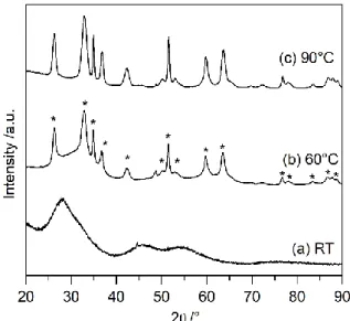
The effect of the reaction temperature was assessed and Figure 2 shows the XRD patterns of the compounds obtained after a 24 hours reaction at room temperature, 60 °C and 90 °C. At room temperature, the amorphous phase which is obtained immediately after precipitation (Figure 1a) does not better crystallize when left for 24 hours at room temperature (Figure 2a). Increasing the temperature up to 60 °C leads to the crystallization of the phase, but the reaction is still incomplete after 24 h as attested by the residual amorphous
5
contribution (Figure 2b), which suggests that a longer reaction time is needed to fully crystallize the phase at 60 °C. As discussed above, a reaction temperature of 90 °C considerably increases the kinetics of the reaction and the crystallized BiCuOS powder is obtained as a pure phase, assessed by XRD and SEM-EDX, after a few hours of reaction (Figure 2c). The lattice parameters obtained after a Le Bail fit followed by Rietveld refinement of the pattern are a = b = 3.866(1) Å and c = 8.598(2) Å (Figure S1). Outcome of the Rietveld refinement are presented in Table S1 and S2.
Figure 2. XRD patterns of the mixed precursor solutions maintained for 24 h at (a) room temperature, (b) 60 °C and (c) 90 °C. * gives the peak positions of the BiCuOS phase
(space group P4/nmm). Microstructure
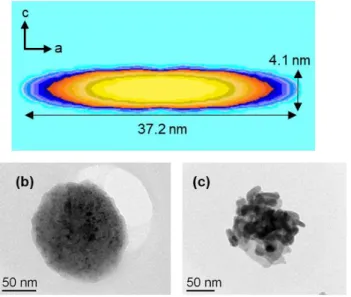
The XRD peak shapes of the phase (90°C for 24h) show some marked anisotropic broadening, as indicated by the broader peaks corresponding to (101), (102), and (111) lines compared to that of the (110) and (200) lines. The peak shapes were modelled using the spherical harmonics expansion implemented in Fullprof (cf. experimental section). Figure 3a presents the visualization, using the GFOURIER program,[18] of the average crystallite size obtained from the refinement. This result testifies of the plate shape of the particles with a larger dimension of the crystallites along the (ab) plane than along the c direction.
TEM images of the powder synthesized at 90 °C just after mixing the reactants and after 4 hours of reaction are shown on Figure 3b and Figure 3c respectively. The aggregate visible on Figure 3b does not enable to identify any particles which is consistent with the presence of an amorphous phase just after the mixing of the reactant. But, after 4 hours of reaction, the aggregate consists of primary platelets of around 5 to 10 nm thick and 20 to
6
30 nm large. This result fits with the anisotropic broadening observed in the XRD peak shapes and the sizes calculated with the Scherrer formula using anisotropic broadening[16] and therefore suggests that the platelets observed on the TEM image are monocrystals.
Figure 3. (a) Visualization of the average crystallite shape obtained from refinement of the spherical harmonic expansion coefficient used to model the peak shapes of the XRD
data. TEM images of samples (b) MP (amorphous phase) and (c) BiCuOS-4h
Optical and electronic properties
In the following of the study, the powder obtained after a reaction time of 4 hours at 90 °C, showing the pure BiCuOS phase, was used. The optical properties of the material were determined by measuring its diffuse reflectance spectra over the visible range (Figure S2). The bandgap energy, calculated thanks to the Tauc formula (cf. Experimental section), is 1.1 ± 0.1 eV, which is consistent with previously reported values in the literature.[8,12] The resistivity of the sample, measured on a pressed pellet is low: 40 Ω·cm at 300 K, which is a typical value for a highly-doped semiconductor. The activation energy calculated from the Arrhenius plot (0.06 eV) is low compared to the bandgap of the material, which is typical of doped semiconductors for which the mobility is controlled by defect states (extrinsic domain).[32] These values match those obtained in the literature for BiCuOS synthesized through conventional solid-state routes.[7,33] We can therefore make the hypothesis that the charge carrier concentration is not too affected by the synthesis procedure.
Thin film deposition
Obtaining nanoparticles of the material was the first step towards the fabrication of thin film pn junctions through liquid- based deposition routes. The second step consisted in
7
creating a stable colloidal suspension of BiCuOS particles in a solvent prior to the coating of the substrate. Stable colloidal suspensions can be obtained by functionalizing the surface of the particles with an organic ligand soluble in the chosen solvent. To avoid the creation of high energy insulating barriers between the grains,[34–36] we used a catechol functionalized poly-3-hexylthiophene (P3HT-Cat).[22] This ligand was proven to adsorb onto zinc oxide surface and to increase electronic transfer from grain to grain by introducing a low energy vacant energetic level between the grains of semiconductor. This method replaces the sintering step[37,38] used to optimize the electrical transport, which cannot be applied for BiCuOS, as it decomposes under such oxidizing conditions.
Figure 4 presents pictures of the suspension just after BiCuOS powder was mechanically dispersed in the solution of P3HT-Cat, and one hour after, showing the stability of the suspension. This suspension could then be used for the deposition of BiCuOS thin film.
Figure 4. Dispersion in THF of P3HT-Cat grafted BiCuOS synthesized through precipitation and evolution of the dispersion stability with time.
In order to test the photoelectric properties of BiCuOS, a pn junction was made. ZnO was chosen as the n-type layer to be associated with BiCuOS as a previous study showed that this combination leads to the best theoretical efficiency as opposed to other semiconductor such as SiC, CdS or GaAs.[5,6] Figure 5 presents a SEM micrograph of the ZnO/BiCuOS junction deposited onto a FTO/glass substrate, showing a 400 nm thick and porous BiCuOS film.
8
Figure 5. Cross section SEM image of the FTO-ZnO-BiCuOS layered film.
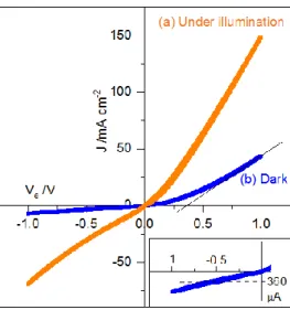
The intensity potential curve of the pn junction without any illumination is presented on Figure 6. As a comparison, the intensity potential curves of both materials in separate thin films was measured (Figure S3). Both thin films taken separately show the characteristic of a resistance with ohmic contacts for BiCuOS and rectifier contacts for ZnO. In both cases, a symmetric behavior is observed. On the contrary, when the two thin films are assembled in a junction, the intensity potential curve in the dark (Figure 6b) shows the behavior of a diode working in the forward direction for V > Vthreshold and reverse direction for V < Vthreshold. This
is typical of the presence of an energy barrier at the interface caused by the equilibration of Fermi levels and interfacial charge transfer thermodynamically imposed by the difference in charge carriers type and concentration between the two materials.[39,40] Because BiCuOS and ZnO are semiconductors (Figure S2) and previously identified as p-type for BiCuOS and n-type for ZnO, the formation of a pn junction is believed to be responsible for this diode characteristic. A schematic layout of the band structure at the interface is reproduced on Figure S4, and explains the formation of the energy barrier at the interface. The saturating current in the reverse direction is in average of 360 μA (insert on Figure 6). This value is high compared to that of commercial diodes and literature data (in the nA order of magnitude). This leakage current is probably due to the low density of the film. The built-in potential is Vthreshold = 0.36 V, which is comparable to commercial silicon or germanium diode for which
the built-in potential is of 0.6 and 0.3 V respectively. The dynamic resistance, rd, of the diode,
corresponds to the inverse of the curve tangent for a given voltage. For V = 0.75 V, rd = 160 Ω. This value is high compared to commercial diodes (of only a few ohms), and
9
Figure 6. Current vs. voltage plot of the ZnO/BiCuOS junction (a) under illumination of a 300 W Xe lamp and (b) in the dark. Scan speed is 20 mV·s-1 and sample surface is
S = 0.1 cm2. Zoom on the saturation current in the dark (insert)
When illuminated (Figure 6a), the junction does not show any photovoltaic effect, corresponding to the creation of a photocurrent for an applied potential of 0 V, which means that the photogenerated charges cannot be extracted. Once excited by the incident radiation, the charge recombines with defects such as ionized centers (vacancies), dislocations, grain boundaries, impurity phases, which then cancels out the photocurrent. Also, as reported elsewhere, [13] the p-type charge carrier concentration in the BiCuOS layer may be too elevated leading to a too thin space charge layer at the n-p junction. This is the region where the photovoltaic effect should take place. Therefore, for the charges to be collected, it is necessary to apply a potential and we observe a drastic increase of the current over the whole voltage range under illumination. The increase in current is linked to the increase of the conductivity of both semiconductors under illumination (photoconductivity). For V = - 0.5 V, the current under illumination is -31 mA·cm-2. The photocurrent, Iph, is │ 31
Idark│= 30.6 mA·cm-2, which corresponds to an increase of a factor 85 compared to that in
dark conditions: Iph/│Idark│= 85. This photoconductivity effect represents a substantial
increase compared to that of BiCuOS measured separately, previously reported, for which Iph/Idark = 0.5.[41] The junction is therefore strongly photosensitive and could be used as a
photodetection device for instance. The most common inorganic phases reported as p-type absorber layers in photodiode or photovoltaic pn junctions are Si, GaAs, CdTe, InP, CuInSe2,
Zn3P2, CIGS (CuInxGaySe), CZTS (Cu2ZnSnS4), WSe2…[42,43] BiCuOS stands out as an
interesting alternative, as being composed of abundant and environmentally friendly elements as well as being extremely stable towards hydrolysis and O2 oxidation at room temperature.
10
C. Conclusion
To conclude, we have developed a new synthesis method for stabilizing soluble bismuth and copper (I) precursors in basic aqueous solutions. It allowed the preparation of BiCuOS nanoparticles under soft conditions using water as a solvent and very low temperatures (60 to 90 °C). It is easy to set up, environmentally friendly, and can be easily applied for large scale synthesis. The obtained nanoparticles show a platelet morphology, of around 5 nm thick and 25 nm large, which is expected considering the layered structure of the material. A stable colloidal suspension could be obtained with the help of a catechol functionalized poly-3-hexylthiophene (P3HT-Cat) that can act both as a colloid stabilizer and as an electron transfer molecule in the films.
In this study, we have contributed and proposed a solution to the great problem of depositing thin films of sulfide materials using low temperature methods, which is crucial for the industrial development of non-oxide materials at lower costs. More efforts are necessary to obtain a photovoltaic effect with such conducting films deposited at low temperature, especially targeting higher layer homogeneity, as well as improving both the mechanical strength and the film roughness.
D. Experimental Materials
Bismuth nitrate Bi(NO3)3 (99 %, Sigma Aldrich), nitric acid HNO3 68% (AnalaR
NORMAPUR, VWR), sodium hydroxide NaOH (99 %, VWR), tartaric acid C4H4O6 (99,5 %
Sigma Aldrich), copper sulfate pentahydrate CuSO4•5H2O (AnalaR NORMAPUR, VWR),
ammonium hydroxide NH4OH 28% (NORMAPUR, VWR), sodium thiosulfate
Na2S2O3•5H2O (99,5%, Sigma Aldrich), sodium sulfide nonahydrate Na2S•9H2O (99 %,
Sigma Aldrich), THF (RP-NORMAPUR, VWR), Zn(CH3CO2)2•2H2O (98%, Sigma Aldrich).
Synthesis
In a 25 mL beaker, 0.728 g of Bi(NO3)3 is dissolved in 10 mL of a 1.8 M diluted nitric
acid aqueous solution. In a 250 mL round bottom flask, 2.156 g of NaOH and 1.124 g of tartaric acid are dissolved in 30 mL of distilled water. Under magnetic agitation, the acidic bismuth solution is slowly poured into the alcaline tartrate solution. A white precipitate, corresponding to bismuth hydroxide Bi(OH)3, forms instantaneously and rapidly disappears
11
In a 50 mL round bottom flask, 0.478 g of CuSO4•5H2O is dissolved in 30 mL of
distilled water. Under magnetic stirring, 1.9 mL of an ammonium hydroxide solution NH4OH
28% is added to the copper solution. The solution instantaneously turns to a dark blue color, testifying the formation of the Cu(NH3)42+ complex. 3.3 g of Na2S2O3•5H2O is then swiftly
added. The solution is slowly heated to 60 °C thanks to an oil bath and maintained under magnetic stirring at this temperature. The solution slowly lightens, and after few hours, once a clear solution is obtained, the reaction is quenched by cooling the flask into an ice bath.
The copper solution is then added to the bismuth solution under magnetic stirring, and immediately 20 mL of a 0.15 M Na2S aqueous solution is swiftly incorporated to have each
element (Bi, Cu and S) at a concentration of 0.03 M. A black precipitate forms instantaneously. The mixture is maintained under magnetic stirring at a chosen temperature and for a determined time. The suspension is then cooled down, filtered thanks to a Büchner filtering device, and the powder is washed with 3 times 25 mL of distilled water before being dried in an oven at 65 °C for 12 hours. A black powder, consisting of BiCuOS nanoparticles, is then recovered.
XRD
X ray diffraction (XRD) experiments were carried out in Bragg-Brentano geometry on a Panalytical X’Pert Pro apparatus with monochromated CuKα1 beam in the 8 ≤ 2θ ≤ 140 °
scan range, step δ2θ = 0.013 °, with a total counting time of 13 h.
The program FullProf[44] was used to refine lattice parameters and obtain information about the microstructure. Microstructural information can be obtained thanks to the method described by Rodriguez-Carjaval et al.[45] In that matter, peak shapes were modelled using the spherical harmonics expansions[46] in a tetragonal material with Laue class 4/m. This model uses the Scherrer formula, which considers that the size broadening can be written as a linear combination of spherical harmonics. The microstructural information given in the output files were then treated using GFOURIER program[47] to visualize the particle shapes.
Transmission Electron Microscopy
Size and morphology of the objects were determined using a Transmission Electron Microscope (JEOL JEM-2000 FX electron microscope operating at 200 KeV). In these experiments, the powder was dispersed in ethanol and a drop placed on a 300-mesh carbon-coated copper grid (Agar scientific) before drying.
12
The optical properties of the powders were investigated by diffuse reflectance spectroscopy with a Cary 5000 UV-Vis-NIR spectrophotometer (Agilent Technologies) equipped with an integrating sphere. Reflection data have been treated following a combined approach of the Tauc[48] and the Kumar method.[49] Indeed, the absorbance of the material is proportional to
where is the diffuse reflexion intensity, and the
maximum and minimum reflectances. As for an indirect bandgap material, one can write following Tauc formula Therefore, if we plot the square root of
vs. , the bandgap of the material can be obtained as the extrapolation of a
straight line to the zero value of the ordinates.
Transport properties
Resistivity was measured down to liquid nitrogen by the four-point method on a sample pelletized at 300 MPa (relative density 60%) using a laboratory made set-up using a Keithley K2700 conductimeter. Contacts were made with a silver paint (purchased from SPI supplies).
Fabrication of the pn junction
The pn junction was fabricated first by depositing a zinc oxide layer onto a commercial fluorine-doped tin oxide (FTO, front electrode) coated glass wafer, then by depositing the BiCuOS nanoparticle layer through spin coating onto the ZnO film, and finally by depositing a gold layer (back electrode) through thermal evaporation.
The zinc oxide thin film was made through the sol-gel method[50] by spin coating. 5.487 g of zinc acetate (0.5 M) are dissolved in 50 mL of absolute ethanol under magnetic agitation in a 100 mL round bottom flask. 1.53 mL of monoethanolamine (0.5 M) are added to the solution in order to obtain uniform sized ZnO nanoparticles. The solution is refluxed at 80 ºC for 3 hours. FTO coated glass slides were washed with soap water, acetone and ethanol successively in an ultrasonic bath for 5 min and then dried in air. The deposition is made by spin coating the ZnO suspension on the substrate at 3000 rpm for 20 s, then 400 rpm for 10 s. The coating is then dried at 300 °C for 10 min in air in order to evaporate monoethanolamine. The procedure is repeated 10 times in order to obtain the desired thickness. The coating is then sintered at 400 °C for 2 hours.
The deposition of BiCuOS thin film requires first to stabilize the colloidal suspension, which was performed by using a catechol functionalized poly-3-hexylthiophene (P3HT-Cat).
13
The synthesis method as well as the characterization of the molecule can be found elsewhere[51] using a polymerization degree of 25. This additive acts both as a colloidal stabilizer and as an intergranular transport enhancer.
Then, a solution containing 0.1 g·L-1 of P3HT-Cat dissolved in THF is prepared. 30 mg of BiCuOS powder (synthesized using the method described above, at 90 °C for 4 hours) is then added to 3 mL of this solution (10 mg·mL-1). The suspension is stirred in an ultra-sonic bath for a few minutes. A stable colloidal suspension is obtained. Deposition of this suspension onto the ZnO layer is performed by spin-coating at 2000 rpm for 20 s during which 100 μL of the suspension are added drop-by-drop. The coating dries instantaneously and the process is repeated 10 times in order to obtain the desired thickness.
Scanning Electron Microscopy
Scanning electron microscopy (SEM) photographs were taken with a LEO 1530 (Zeiss) instrument, operating at 15 keV and equipped with an In-lens detector. Elemental analysis was performed with EDS using an X Ray detector (Centaurus).
Photoelectric properties measurement
The junction was illuminated with a Xe visible lamp 300 W by placing the FTO side of the device towards the lamp at a distance of 25 cm. The beam illuminates the whole surface of the sample (0.1 cm2). The current passing through the junction is recorded as a function of the voltage [-1 V; 1 V] thanks to a VMP-3 potentiostat (Bio-Logic instrument).
Supporting information
Rietveld refinement, Optical and Electronic properties.
Acknowledgment
We thank the French National Research and Technology Agency (ANRT) for the funding.
Keywords
Nanostructures, oxysulfides, photoelectric properties, precipitation synthesis, thin films
14
[1] A. M. Kusainova, P. S. Berdonosov, L. G. Akselrud, L. N. Kholodkovskaya, V. A. Dolgikh, B. A. Popovkin, J. Solid State Chem. 1994, 112, 189–191.
[2] D. Berthebaud, E. Guilmeau, O. I. Lebedev, A. Maignan, J. Gamon, P. Barboux, J. Solid
State Chem. 2016, 237, 292–299.
[3] C. Barreteau, D. Bérardan, E. Amzallag, L. Zhao, N. Dragoe, Chem. Mater. 2012, 24, 3168–3178.
[4] M. U. Farooq, S. Butt, K. Gao, X. L. Pang, X. Sun, Asfandiyar, F. Mohmed, A. Ahmad, A. Mahmood, N. Mahmood, J. Alloys Compd. 2017, 691, 572–577.
[5] T. Le Mercier, P. Barboux, T. Le Bahers, C. N. D. L. R. S. Rhodia Operations, Mixed
Bismuth and Copper Oxides and Sulphides for Photovoltaic Use, 2014, WO2014049172
A2.
[6] T. Le Bahers, S. Haller, T. Le Mercier, P. Barboux, J. Phys. Chem. C 2015, 119, 17585– 17595.
[7] S. K. Karna, C.-W. Wang, C.-M. Wu, C.-K. Hsu, D. Hsu, C.-J. Wang, W.-H. Li, R. Sankar, F.-C. Chou, J. Phys. Condens. Matter 2012, 24, 266004.
[8] H. Hiramatsu, H. Yanagi, T. Kamiya, K. Ueda, M. Hirano, H. Hosono, Chem. Mater.
2008, 20, 326–334.
[9] H. Zhu, T. Su, H. Li, C. Pu, D. Zhou, P. Zhu, X. Wang, J. Eur. Ceram. Soc. 2017, 37, 1541–1546.
[10] J.-B. Labégorre, R. Al Rahal Al Orabi, A. Virfeu, J. Gamon, P. Barboux, L. Pautrot-d’Alençon, T. Le Mercier, D. Berthebaud, A. Maignan, E. Guilmeau, Chem. Mater.
2018, 30, 1085–1094.
[11] A. Ubaldini, E. Giannini, C. Senatore, D. Van Der Marel, Phys. C Supercond. 2010, 470, S356–S357.
[12] W. C. Sheets, E. S. Stampler, H. Kabbour, M. I. Bertoni, L. Cario, T. O. Mason, T. J. Marks, K. R. Poeppelmeier, Inorg. Chem. 2007, 46, 10741–10748.
[13] J. Gamon, S. Haller, E. Guilmeau, A. Maignan, T. Le Mercier, P. Barboux, J. Solid State
Chem. 2018, 263, 157–163.
[14] H. Li, V. Lesnyak, L. Manna, in Large Area Flex. Electron. (Eds.: M. Caironi, Y.-Y. Noh), Wiley-VCH Verlag GmbH & Co. KGaA, Weinheim, Germany, 2015, pp. 163– 186.
[15] E. S. Stampler, W. C. Sheets, M. I. Bertoni, W. Prellier, T. O. Mason, K. R. Poeppelmeier, Inorg. Chem. 2008, 47, 10009–10016.
[16] C. Doussier-Brochard, B. Chavillon, L. Cario, S. Jobic, Inorg. Chem. 2010, 49, 3074– 3076.
[17] X. Fang, T. Zhai, U. K. Gautam, L. Li, L. Wu, Y. Bando, D. Golberg, Prog. Mater. Sci.
2011, 56, 175–287.
[18] N. G. Deshpande, A. A. Sagade, Y. G. Gudage, C. D. Lokhande, R. Sharma, J. Alloys
Compd. 2007, 436, 421–426.
[19] Y. Shi, Z. Jin, C. Li, H. An, J. Qiu, Appl. Surf. Sci. 2006, 252, 3737–3743. [20] X.-H. Li, H.-B. Li, G.-D. Li, J.-S. Chen, Inorg. Chem. 2009, 48, 3132–3138. [21] P. Kumar, M. Gusain, R. Nagarajan, Inorg. Chem. 2011, 50, 3065-3070.
15 [22] E. Peters, Metall. Trans. B 1976, 7, 505–517.
[23] N. Takeno, Atlas of Eh-pH diagrams - Intercomparison of thermodynamic databases, Geological Survey of Japan Open File Report No.419, 2005. [URL] https://www.nrc.gov/docs/ML1808/ML18089A638.pdf
[24] M. Bobtelsky, J. Jordan, J. Am. Chem. Soc. 2002, 69, 2286-2290. [25] P. G. Manning, Can. J. Chem. 1963, 41, 2557–2565.
[26] L. E. Warren, J. Am. Pharm. Assoc. 1925, 14, 478–487.
[27] "5N Plus, specialty metals and chemicals supplier", can be found under https://www.5nplus.com/
[28] B. Laik, P. Poizot, J.-M. Tarascon, J. Electrochem. Soc. 2002, 149, A251–A255. [29] T. P. Hoar, G. P. Rothwell, Electrochimica Acta 1970, 15, 1037–1045.
[30] H. C. Zhi Sun, H. C. Zhi Sun, Front. Chem. Sci. Eng. 2017, 11, 308–316.
[31] G. Milazzo, S. Caroli, R. D. Braun, J. Electrochem. Soc. 1978, 125, 261C-261C.
[32] B. Van Zeghbroeck, Principle of Semiconductor Devices, University of Colorado, 2011. [URL] http://ecee.colorado.edu/~bart/book/.
[33] D. Berardan, J. Li, E. Amzallag, S. Mitra, J. Sui, W. Cai, N. Dragoe, Materials 2015, 8, 1043–1058.
[34] S. E. Habas, H. A. S. Platt, M. F. A. M. van Hest, D. S. Ginley, Chem. Rev. 2010, 110, 6571–6594.
[35] M. V. Kovalenko, M. Scheele, D. V. Talapin, Science 2009, 324, 1417–1420.
[36] J. W. Cho, A. Ismail, S. J. Park, W. Kim, S. Yoon, B. K. Min, ACS Appl. Mater.
Interfaces 2013, 5, 4162–4165.
[37] M. Law, J. M. Luther, Q. Song, B. K. Hughes, C. L. Perkins, A. J. Nozik, J. Am. Chem.
Soc. 2008, 130, 5974–5985.
[38] M. N. Kamalasanan, S. Chandra, Thin Solid Films 1996, 288, 112–115.
[39] S. J. Fonash, in Sol. Cell Device Phys. (Ed.: S.J. Fonash), Academic Press, 1981, pp. 187–261.
[40] T. F. Schubert, E. M. Kim, Synth. Lect. Digit. Circuits Syst. 2016, 11, 1–266.
[41] J. Gamon, D. Giaume, G. Wallez, J.-B. Labégorre, O. I. Lebedev, R. Al Rahal Al Orabi, S. Haller, T. Le Mercier, E. Guilmeau, A. Maignan, P. Barboux, Chem. Mater. 2018, 30, 549–558.
[42] S. R. Kodigala, in Thin Films Nanostructures (Ed.: S.R. Kodigala), Academic Press,
2010, pp. 1–19.
[43] A. Fahrenbruch, R. Bube, Fundamentals Of Solar Cells: Photovoltaic Solar Energy
Conversion, Elsevier, 2012.
[44] J. Rodriguez-Carvajal, FULLPROF Program version September 2019, ILL (unpublished).
[45] J. Rodriguez-Carvajal, FULLPROF Manual version September 2019, ILL (unpublished). [46] M. Jarvinen, J Appl Cryst 1993, 26, 527.
16
[47] J. Gonzalez-Platas, J. Rodriguez-Carjaval, GFourier: a Windows/Linux program to calculate and display Fourier maps. Program available within the FullProf Suite. [URL]
https://www.ill.eu/sites/fullprof/php/programse811.html?pagina=Fourier [48] J. Tauc, R. Grigorovici, A. Vancu, Phys. Status Solidi 1966, 15, 627.
[49] V. Kumar, S. Kr. Sharma, T. P. Sharma, V. Singh, Opt. Mater. 1999, 12, 115–119. [50] R. M. Pasquarelli, D. S. Ginley, R. O’Hayre, Chem. Soc. Rev. 2011, 40, 5406–5441. [51] J. Gamon, C. Robert, T. Le Mercier, P. Barboux, C. M. Thomas, D. Giaume, Mater.
Chem. Phys. 2019, 232, 400–408.
Table of Content Graphical Abstract
Oxysulfide BiCuOS nanoparticles were synthesized through a well-controlled low temperature wet chemistry route in water. A thin film of these nanoplatelets was then obtained
via the deposition of a colloidal ink onto an FTO/ZnO substrate to form a pn junction. This acts as a strongly photosensitive diode with Iph/Idark = 85, corresponding to an increase of more