HAL Id: hal-00817117
https://hal.archives-ouvertes.fr/hal-00817117
Submitted on 23 Apr 2013
HAL is a multi-disciplinary open access
archive for the deposit and dissemination of
sci-entific research documents, whether they are
pub-lished or not. The documents may come from
teaching and research institutions in France or
abroad, or from public or private research centers.
L’archive ouverte pluridisciplinaire HAL, est
destinée au dépôt et à la diffusion de documents
scientifiques de niveau recherche, publiés ou non,
émanant des établissements d’enseignement et de
recherche français ou étrangers, des laboratoires
publics ou privés.
Fast All-Optical 10 Gb/s NRZ Wavelength Conversion
and Power Limiting Function using Hybrid InP on SOI
Nanocavity
Kevin Lenglé, Mathilde Gay, A. Bazin, Isabelle Sagnes, Remy Braive, Paul
Monnier, Laurent Bramerie, Thanh Nam Nguyen, Christelle Pareige, Robert
Madec, et al.
To cite this version:
Kevin Lenglé, Mathilde Gay, A. Bazin, Isabelle Sagnes, Remy Braive, et al.. Fast All-Optical 10 Gb/s
NRZ Wavelength Conversion and Power Limiting Function using Hybrid InP on SOI Nanocavity.
European Conference on Optical Communication (ECOC 2012), Sep 2012, Amsterdam, Netherlands.
pp.We.2.E.5, �10.1364/ECEOC.2012.We.2.E.5�. �hal-00817117�
Fast All-Optical 10 Gb/s NRZ Wavelength Conversion and
Power Limiting Function using Hybrid InP on SOI Nanocavity
K. Lenglé(1,2), M. Gay(1,2), A. Bazin(3), I. Sagnes(3), R. Braive(3), P. Monnier(3), L. Bramerie(1,2), T-N Nguyen(1,2), C. Pareige(1,2), R. Madec(1,2), J-C. Simon(1,2), R. Raj(3), F. Raineri(3,4)
(1)
Université Européenne de Bretagne (UEB,) 5 Boulevard Laënnec, 35000 Rennes, France, [email protected]
(2)
CNRS-Foton Laboratory (UMR 6082), Enssat, BP 80518, 22305 Lannion Cedex, France
(3)
Laboratoire de Photonique et de Nanostructures, CNRS-UPR20, Route de Nozay, 91460 Marcoussis, France, [email protected]
(4)
Université Paris Diderot, 75207 Paris Cedex 13, France
Abstract A new optical switch is presented using InP/SOI hybrid photonic crystal nanocavity.
Switching contrast of 11 dB with 20 mW peak power and recovery time of 14 ps are measured. NRZ wavelength conversion and power limiter are demonstrated at 10 Gb/s through system experiments with 6 and 1 mW peak power respectively.
Introduction
InP/Silicon on Insulator (SOI) hybrid technology is an extremely promising solution for future photonic circuits as it combines CMOS compatibility with optoelectronic properties of III-V materials. Microdisks fabrication recently allowed the demonstration of lasers, amplifiers, modulators, flip-flops [1], wavelength converters [2] and modulation formats converters [3]. The integration of photonic crystal (PhC) nanolaser on top of SOI waveguides further demonstrated the potential of this technology towards nanophotonic components [4]. In this paper, we demonstrate for the first time wavelength conversion and power limiting function in a system experiment at 10 Gb/s using a PhC nanocavity based on III-V/SOI hybrid technology which incorporates an active material optimized for ultrafast operation.
Device description
The structure designed and fabricated at CNRS-LPN is composed of two optical levels: the first one is a single mode SOI wire waveguide and the other one is an InP-based PhC nanocavity (Fig.1). The two levels are separated by a low index layer (silica + benzocyclobutene) which preserves the vertical optical confinement within the SOI waveguide and the PhC cavity. Optical coupling between the two levels, measured to be 90 % [4], is ensured by the penetration of the evanescent tail of the optical modes into the other level.
The studied nanocavity is a “wire” or “nanobeam” [5] cavity, Fabry-Perot (FSR ~ 29 nm) which is formed by drilling holes in a single mode InP wire waveguide (600 nm x 260 nm) where a single InGaAs quantum well (QW) (8 nm) is grown at both surfaces. The cavity is fully encapsulated in SiO2 in order to increase
heat sinking which usually hampers operation at high bit rates. Its design is based on the use of Gaussian apodization of the electromagnetic field profile within the cavity [6] offering the possibility of Q factors higher than 106 with modes close to 1.55 µm where the absorption edge of the QWs is positionned. Grating couplers are etched at each extremity of the SOI waveguide to allow coupling with cleaved facet single mode optical fibers [7]. Details on a similar device can be found in [4].
Fast switching operation
Switching is obtained by inducing a change in refractive index within the III-V material by increasing the power of a control beam (here the pump). Indeed, the pump is directly absorbed by the surface quantum wells modifying the carrier density, thereby the refractive index and the cavity resonance wavelength. Ultrafast carrier recombination is expected because of the enhancement of non radiative recombination obtained by placing the QWs at the very surface of the structure and by patterning the material with dimension smaller than the carrier diffusion length.
Fig. 2 inset shows the spectral transmission curve at low incident power (no switching). In
Grating coupler PhC nanocavity
Grating coupler PhC nanocavity
the considered wavelength range, two resonances are measured, the 1st one at 1540 nm and the second one at 1569 nm, the spacing corresponding to the free spectral range of the Fabry-Perot cavity. The switching of the cavity can be obtained by exciting one cavity or the other indifferently. The minimum fiber-to-fiber insertion losses is 14 dB and mainly comes from fiber-to-waveguide coupling losses (7 dB per side), as it was shown in [4] that the coupling from the SOI waveguide to the InP PhC cavity was 90 %.
Two kinds of co-propagative two color pump-probe experiments are performed. In order to determine the time response of the cavity, a 10 GHz mode locked laser generating 3 ps pulses was used; the repetition rate was decreased down to 500 MHz (using a MZI external modulator) in order to reach a high peak power. In this pump probe experiment, pump and probe were located around the 1st resonance (pump at 1545 nm, probe at 1540 nm), as neither our optical sampling oscilloscope (OSO) nor our short pulsed source works in the L-band (where the 2nd resonance is located). The modulated probe measured with an OSO with 1 ps resolution is shown on Fig. 2, where T is the signal transmission and T0 the transmission with no pump signal. Time response is deduced from a 2 level carrier density model by considering a single time constant in a first approximation. A very fast recovery time of 14 ps was measured in both switch-on and -off configurations.
In the second pump probe experiment the possibility to use both resonances for pumping and probing was explored. In this experiment the pump consisted in 100 ps pulses generated by a CW laser modulated in an external modulator at 10 Gb/s. The repetition rate was divided by a factor of 20 by the same technique as in the 1st pump probe experiment to decrease the repetition rate down to 500 MHz. By probing at the 2nd resonance and pumping at the 1st one, we obtained a switching contrast of 11 dB with
20 mW coupled peak power; the resonance depth is reached as shown on the transmission of the cavity in the Fig.2 inset. The functionality of the device was then tested in system experiments.
Two functions whose principles are displayed in Fig.3 were tested. In the wavelength conversion case, when the cavity resonance is blue-shifted dynamically under a pump pulse action, the probe transmission increases, hence “copying” the signal at the probe wavelength. In the case of power limiting function, the incoming signal “self-switches” the cavity transmission: high power levels switch more the resonance than low power levels; hence transmission of high power levels is lower than transmission of low power levels, thus limiting the signal amplitude fluctuations.
NRZ wavelength converter at 10 Gb/s
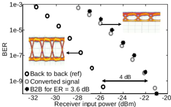
In this experiment a 10 Gb/s PRBS sequence was used as the pump signal at the 2nd resonance and a CW signal as the probe signal at the 1st resonance, in order to favour a better signal to noise ratio. At the maximum available pump power (corresponding to a coupled peak power of 6 mW) a clearly open converted eye diagram was obtained (Fig. 4). Bit Error Rate (BER) measurements show error free operation on the converted signal (grey empty circles).
However a 4 dB penalty is measured at a BER of 10-9 owing to a low converted signal extinction ratio as demonstrated by the BER measurement of the back to back with a degraded extinction ratio of 3.6 dB (full symbols). Indeed in this configuration, the highest coupling losses at the pump wavelength make the pump less efficient for the same mean power at the input of the device. This should be improved in the near
1500 200 250 300 350 400 0.2 0.4 0.6 0.8 1 Time(ps) (T -T 0 )/ T 0 Experiment 2 levels model =14 psτ 1530 1540 1550 1560 1570 1580 -30 -25 -20 -15 W avelength (nm ) T ra n s m is s io n ( d B ) 11 dB
Fig. 2: Converted probe (switch on). Cavity transmission in the inset.
-32 -30 -28 -26 -24 -22 -20
1e-9 1e-7 1e-5 1e-3
Receiver input power (dBm)
B
E
R
Back to back (ref) Converted signal B2B for ER = 3.6 dB
4 dB
Fig. 4: BER curves of the converted signal.
Pump Probe
No pump
With pump No signal
Low ‘1’ High ‘1’
Wavelength conversion principle Noise limiter principle
Signal
Fig. 3: Principle of wavelength conversion and power limiter.
future by a better optimization of the structure for this targeted application.
Power limiting function
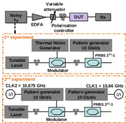
Amplitude fluctuations were generated by two different ways as shown on Fig.5. In the first experiment, intensity noise is generated using a CW laser modulated through an external modulator driven by a 1 GHz bandwidth noise diode. The relative intensity noise (RIN) of this signal is hence varied by adjusting the noise diode voltage.
This optical noisy source is then modulated at 10 Gb/s with a sequence length of 231-1 bits into a second modulator and injected into the component at a slightly blue shifted wavelength towards the cavity resonance. In Fig.6, we can clearly see on the eye diagrams the amplitude noise reduction at the output of the device.
Signal to noise ratio (SNR) values come from average level and standard deviation figures measured on histograms of mark levels. The output SNR as a function of the input SNR curve clearly shows noise reduction as it is located above the linear transmission curve (slope 1).
In the second experiment, to increase the noise bandwidth, we substitute the noise diode by a second 10 Gb/s pattern generator (27-1 PRBS
sequence) without any synchronisation with the pattern generator used for BER measurements owing to a 15 MHz frequency shift (Fig. 5, 2nd experiment). Fig. 7 shows a BER measurement with the back to back (crosses), the degraded signal (grey circles) and regenerated one (black circles). This measurement shows a penalty reduction of 4.5 dB at 10-9 BER with a coupled peak power as low as 1 mW.
Conclusions
We report for the first time fast switching in a system experiment using a hybrid InP-based PhC nanocavity integrated on a SOI waveguide. Switching contrast of 11 dB and time recovery of 14 ps are obtained. This structure is used for NRZ wavelength conversion and also for power limiting function at 10 Gb/s, thereby allowing a noise reduction capability. These noteworthy results demonstrate the huge possibilities of nanophotonics III-V/SOI technologies for all optical signal processing in very small footprints, and low energy consuming components.
Acknowledgements
We acknowledge the support by the European Union, FP7/ICT funding programme, under the
Copernicus project (249012)
(www.copernicusproject.eu). This work is also
supported by Region Bretagne and ANR Jeunes Chercheurs PROWOC. The SOI wafers were fabricated within the ePIXfab European silicon platform.
References
[1] D.Van Thourhout et al, JSTQE, 16, 5, (2010). [2] R. Kumar et al, Opt. Lett. 36, 13 (2011). [3] R. Kumar et al, Opt. Exp. 19, 10 (2011). [4] Y. Halioua et al, Opt. Exp., 19, 10 (2011). [5] P. R. Villeneuve et al, Nature 390, 6656
(1997).
[6] Y. Tanaka et al, 26, 11 (2008).
[7] D. Taillaert et al, J. Appl. Phys., 45, 8A (2006). Polarisation controller DUT EDFA Noisy Tx Noisy Tx RxRx 1stexperiment Variable attenuator Modulator PRBS 231-1 Pattern generator 10 Gbit/s Tunable Laser Thermal Noise Generator Modulator CLK1 = 10,66 GHz PRBS 231-1 CLK2 = 10,675 GHz 2ndexperiment Pattern generator 10 Gbit/s Pattern generator 10 Gbit/s S S Tunable Laser
Fig. 5: Experimental setup for the noise limiter.
0 50 100 150 200 250 0 100 200 300 400 SNRin S N R o u t Experiment Linear transmission IN OUT
Fig. 6: Output SNR versus input SNR. Inset: Eye diagrams at input SNR = 34 -35 -30 -25 -20 10-10 10-8 10-6 10-4
Receiver input power (dBm)
B
E
R
Back to back (ref) Degraded signal Regenerated signal
4.5 dB Degraded
Regenerated