ISMRE2018/XXXX-2018 ALGERIA
The thickness effect of ZnO thin films on optical
Properties deposited by spray pyrolysis
Farid Khediri
1, Abdekader Hafdallah
1and Mouna Bouhelal
11
Applied and Theoretical Physics Laboratory, Department of Material Sciences, University Larbi Tebessi - Tebessa, 12002
Tebessa, Algeria
………
khediri_adel@yahoo.fr
Abstract—Much attention has been lead up the transparent
conducting oxides (TCOs) in recent years due to their
interesting physical properties, which combine electrical
conductivity and optical transparency in the spectral range of
the visible. Among these oxides zinc oxide ZnO is with the
properties optical and electric has attracted the attention of
researchers for a long time. In this work Zinc oxide thin films
prepared by spray pyrolysis technique. A set of ZnO thin films
were deposited with various deposition time, on glass substrate
at 350 °C. The precursor solution is formed with zinc acetate in
distilled methanol with 0.1 molarity. The deposition time was
ranged from 2 to 8 min. The optical properties of those films
were examined by ultraviolet-visible spectrometer (UV). ZnO
thin films were highly transparent in the visible with the
maximum transmittance of 85% and the optical band gap was
found between 3.25 and 3.28 eV.
Keywords—Spray pyrolysis, Zinc oxide, thin films, optical
properties.
I.
I
NTRODUCTIONTCOs have been integrated in several fields such as:
transistors [1,2], solar cells [3], organic light emitting diodes,
and electrochromic windows [4]. Among these oxides zinc
oxide ZnO is with the properties optical and electric has
attracted the attention of researchers for a long time, its
thermal and chemical stability very high, it’s no toxicity like
its abundance in the nature more. Zinc oxide has found
special interest for several applications such as a transparent
conducting film for displays and photovoltaic panels [5-6].
LEDs and the inexpensive transistors [7-9] , gas sensing
detectors [10], spintronics [11], smart textiles [12,13]. Many
methods were employed to produce the ZnO thin films such
as magnetron sputtering [14-15], sol–gel, CVD [16], RF
sputtering [17], hydrothermal [18], atomic layer epitaxy [19],
pulsed laser deposition [20-21], spray pyrolysis [22-23].
The spray pyrolysis used to prepare thin films by
directing them to a substrate for depositing thin layers. This
technique can prepare large areas of layers for the
technological applications despite the simplicity of its
equipment, making it important in the industrial vision, and it
can prepare high quality layers with the ability to control the
thicknesses and quality by the process parameters such as,
distance between nozzle orifice and substrate surface, nozzle
shape and dimensions, precursor material and concentration,
flow rates of gas and solution, spray time and substrate
temperature [24-26].
The aim of this work is to study the optical properties of
ZnO thin films prepared by spray pyrolysis method under
different spray times. Transmittance measurements under
UV-Visible. The evolution of the properties of the sprayed
ZnO films is discussed and correlated to the deposition
conditions.
II.
E
XPERIMENTAL DETAILSZnO thin films were grown onto glass substrate, using a
spray pyrolysis technique. A solution of 0.1 morality was
prepared
by
dissolving
zinc
acetate
dihydrate
C
4H
6O
4Zn.2H
2O precursor in a methanol CH
4O. The
substrates temperature was fixed at 350 ◦C. A set of samples
was prepared by varying the deposition time Td in the range
of 2 min-8 min to investigate the influence of deposition time
on the optical properties of ZnO films.
The optical transmission in the UV–visible range (300–
1100 nm) measurements was performed using Shimadzu
UV-1601 PC spectrophotometer. Films thicknesses and
optical band gaps were estimated from fitting optical
transmission data.
III. R
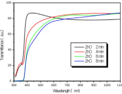
ESULTS AND DISCUSSIONThe optical transmission spectra for as-prepared films
with different deposition time are given in Fig. 1 The average
optical transmittance values of all the films were higher than
75% in the visible light and near infrared regions. The films’
optical transmittances fell off at the UV region with
wavelength shorter than 380 nm. In the UV region with
wavelength lower than 380 nm, the ZnO film showed the
lowest transmittance.
300 400 500 600 700 800 900 1000 1100 0 20 40 60 80 100 Tr an sm itt an ce ( a. u. ) Wavelength ( nm) ZnO 2 min ZnO 4 min ZnO 6 min ZnO 8 minFig. 1. Spectral variation of transmittance with different deposition
time (T
d).
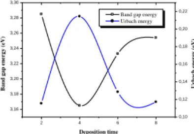
Films optical band gaps are estimated, as shown in Fig. 2
from the plot (αhν)
2as a function of photon energy (hν),
according to Tauc formula for direct band gap
semiconductors [27]:
(αhν)
2= B(Eg - hν)
Localized states appears near the bands edges which
causes band tails formation due to the disorder in film
network. These band tail states are responsible for the photon
absorption in the low energies range. In this range the
absorption coefficient is given by [28]:
(αhν) = α
0exp(hν/E
u)
where α
0is a constant, E
uis disorder energy commonly
called Urbach tail [29].
1,0 1,5 2,0 2,5 3,0 3,5 4,0 4,5 0,0 20,0G 40,0G 60,0G 80,0G 100,0G 120,0G ( h ) 2(c m -2eV 2) h (eV) Td= 2min Td= 4min Td= 6min Td= 8min
Fig. 2. Typical variation of the quantity (ahν)
2as a function of
photon energy.
The variations of the calculated band gap and disorder
energy with deposition time are reported in Fig. 3.
We note a reduction in the gap with the deposition time.
As seen, the variations of both Eg and Eu correlate very well,
this indicates that the variation of the optical gap is governed
by the disorder in the film. Meyer et al. [30].
2 4 6 8 3,16 3,18 3,20 3,22 3,24 3,26 3,28 3,30
Band gap energy Urbach energy Deposition time B a n d g a p e n er g y ( eV ) 0,10 0,12 0,14 0,16 0,18 0,20 0,22 U rb a ch e n er g y ( eV )
Fig. 3. Variation of the optical gap and Urbach energy as a
function of the deposition time.
Authors should discuss the results and how they can be
interpreted in perspective of previous studies and of the
working hypotheses. The findings and their implications
should be discussed in the broadest context possible. Future
research directions may also be highlighted.
IV. C
ONCLUSIONSIn present work, ZnO thin films have been synthesized
using spray pyrolysis technique. The influence of deposition
time on films properties has been investigated. The obtained
results indicate that ZnO films properties are sensitive to the
deposition time. The values of the optical band gap and
Urbach energy change with deposition time. In the visible
region, all the films are highly transparent more than 75%.
R
EFERENCES[1] Y. Sun and J. A. Rogers, “Inorganic semiconductors for flexible electronics,” Adv. Mater., vol. 19, no. 15, pp. 1897–1916, 2007.
[2] J. H. Kim, B. Du Ahn, C. H. Lee, K. A. Jeon, H. S. Kang, and S. Y. Lee, “Characteristics of transparent ZnO based thin film transistors with amorphous HfO2 gate insulators and Ga doped ZnO electrodes,” Thin Solid Films, vol. 516, no. 7, pp. 1529–1532, 2008.
[3] N. Ohashi, K. Kataoka, T. Ohgaki, T. Miyagi, H. Haneda, and K. Morinaga, “Synthesis of zinc oxide varistors with a breakdown voltage of three volts using an intergranular glass phase in the bismuth–boron–oxide system,” Appl. Phys. Lett., vol. 83, no. 23, pp. 4857–4859, 2003.
[4] S. J. Jiao et al., “ZnO p-n junction light-emitting diodes fabricated on sapphire substrates,” Appl. Phys. Lett., vol. 88, no. 3, p. 31911, 2006. [5] T. Kogure and Y. Bando, “Formation of ZnO nanocrystals in the
cubic phase was reported by electron-beam induced oxidation of ZnS surfaces during TEM observations,” J. Electron. Microsc, vol. 47, pp. 7903–7909, 1993.
[6] A. B. M. A. Ashrafi et al., “Growth and characterization of hypothetical zinc-blende ZnO films on GaAs (001) substrates with ZnS buffer layers,” Appl. Phys. Lett., vol. 76, no. 5, pp. 550–552, 2000.
[7] P. Kacman, “Spin interactions in diluted magnetic semiconductors and magnetic semiconductor structures,” Semicond. Sci. Technol., vol. 16, no. 4, p. R25, 2001.
[8] J. K. Furdyna, “Diluted magnetic semiconductors,” J. Appl. Phys., vol. 64, no. 4, pp. R29–R64, 1988.
[9] S. A. Wolf et al., “Spintronics: a spin-based electronics vision for the future,” Science (80-. )., vol. 294, no. 5546, pp. 1488–1495, 2001. [10] H. Hartnagel, A. L. Dawar, A. K. Jain, and C. Jagadish,
Semiconducting transparent thin films. Institute of Physics Bristol, 1995.
[11] D. P. Norton, S. J. Pearton, A. F. Hebard, N. Theodoropoulou, L. A. Boatner, and R. G. Wilson, “Ferromagnetism in Mn-implanted ZnO: Sn single crystals,” Appl. Phys. Lett., vol. 82, no. 2, pp. 239–241, 2003.
[12] Ü. Özgür et al., “A comprehensive review of ZnO materials and devices,” J. Appl. Phys., vol. 98, no. 4, p. 11, 2005.
[13] C. Jagadish and S. J. Pearton, Zinc oxide bulk, thin films and nanostructures: processing, properties, and applications. Elsevier, 2011.
[14] P. F. Carcia, R. S. McLean, M. H. Reilly, and G. Nunes Jr, “Transparent ZnO thin-film transistor fabricated by rf magnetron sputtering,” Appl. Phys. Lett., vol. 82, no. 7, pp. 1117–1119, 2003. [15] L.-Y. Chen, W.-H. Chen, J.-J. Wang, F. C.-N. Hong, and Y.-K. Su,
“Hydrogen-doped high conductivity ZnO films deposited by radio-frequency magnetron sputtering,” Appl. Phys. Lett., vol. 85, no. 23, pp. 5628–5630, 2004.
[16] A. HAFDALLAH, K. DERRAR, M. S. AIDA, and N. ATTAF, “Effet de la solution précurseur sur les propriétés structurales et optiques des couches minces de ZnO préparées par spray pyrolyse,” Afrique Sci., vol. 12, no. 3, pp. 26–33, 2016.
[17] H. S. Yoon et al., “Properties of fluorine doped ZnO thin films deposited by magnetron sputtering,” Sol. Energy Mater. Sol. Cells, vol. 92, no. 11, pp. 1366–1372, 2008.
[18] T. Sekiguchi, S. Miyashita, K. Obara, T. Shishido, and N. Sakagami, “Hydrothermal growth of ZnO single crystals and their optical characterization,” J. Cryst. Growth, vol. 214, pp. 72–76, 2000. [19] Y.-J. Lee et al., “Efficient hydrogenated amorphous silicon thin-film
solar cells using zinc oxide deposited by atomic layer deposition as a protective interfacial layer,” J. Phys. Chem. C, vol. 116, no. 44, pp. 23231–23235, 2012.
[20] V. Craciun, J. Elders, J. G. E. Gardeniers, and I. W. Boyd, “Characteristics of high quality ZnO thin films deposited by pulsed laser deposition,” Appl. Phys. Lett., vol. 65, no. 23, pp. 2963–2965, 1994.
[21] K. L. Narasimhan, S. P. Pai, V. R. Palkar, and R. Pinto, “High quality zinc oxide films by pulsed laser ablation,” Thin Solid Films, vol. 295, no. 1–2, pp. 104–106, 1997.
[22] A. Hafdallah, A. Azzedine, H. Belhani, M. S. Aida, and N. Attaf, “Effect of the Nozzle-Substrate Distance on the Structural and Optical Properties of ZnO Thin Films Deposited by Spray Pyrolysis Technique,” Am. J. Nano Res. Appl., vol. 5, no. 6, p. 87, 2017. [23] M. de la L. Olvera, A. Maldonado, R. Asomoza, M. Konagai, and M.
Asomoza, “Growth of textured ZnO: In thin films by chemical spray deposition,” Thin Solid Films, vol. 229, no. 2, pp. 196–200, 1993.
[24] V. Vasu and A. Subrahmanyam, “Electrical and optical properties of pyrolytically sprayed SnO2 film—Dependence on substrate temperature and substrate-nozzle distance,” Thin Solid Films, vol. 189, no. 2, pp. 217–225, 1990.
[25] Y. S. Sakhare, N. R. Thakare, and A. U. Ubale, “Influence of quantity of spray solution on the physical properties of spray-deposited nanocrystalline MgSe thin films,” Научно-технические ведомости Санкт-Петербургского государственного политехнического университета. Физико-математические науки, no. 1 (237), 2016. [26] W. Sripianem et al., “Effect of aluminium doping concentration on
microstructures, optical and electrical properties of ZnO thin films by spray pyrolysis technique,” Mater. Today Proc., vol. 5, no. 3, pp. 9519–9524, 2018.
[27] L. A. Goodman, “Liquid-crystal displays—Electro-optic effects and addressing techniques,” in Introduction to Liquid Crystals, Springer, 1975, pp. 241–279.
[28] C. M. Lampert, “Heat mirror coatings for energy conserving windows,” Sol. Energy Mater., vol. 6, no. 1, pp. 1–41, 1981. [29] J. Tauc, “Optical properties of amorphous semiconductors,” in
Amorphous and Liquid Semiconductors, Springer, 1974, pp. 159– 220.
[30] F. Urbach, “The long-wavelength edge of photographic sensitivity and of the electronic absorption of solids,” Phys. Rev., vol. 92, no. 5, p. 1324, 1953.