HAL Id: hal-02321139
https://hal.archives-ouvertes.fr/hal-02321139
Submitted on 7 Jul 2020
HAL is a multi-disciplinary open access
archive for the deposit and dissemination of
sci-entific research documents, whether they are
pub-lished or not. The documents may come from
teaching and research institutions in France or
abroad, or from public or private research centers.
L’archive ouverte pluridisciplinaire HAL, est
destinée au dépôt et à la diffusion de documents
scientifiques de niveau recherche, publiés ou non,
émanant des établissements d’enseignement et de
recherche français ou étrangers, des laboratoires
publics ou privés.
Distributed under a Creative Commons Attribution| 4.0 International License
Displacement-Tolerant Printed Spiral Resonator With
Capacitive Compensated-Plates for Non-Radiative
Wireless Energy Transfer
Lai Ly Pon, Sharul Kamal Abdul Rahim, Chee Yen Leow, Mohamed Himdi,
Mohsen Khalily
To cite this version:
Lai Ly Pon, Sharul Kamal Abdul Rahim, Chee Yen Leow, Mohamed Himdi, Mohsen Khalily.
Displacement-Tolerant Printed Spiral Resonator With Capacitive Compensated-Plates for
Non-Radiative Wireless Energy Transfer. IEEE Access, IEEE, 2019, 7, pp.10037-10044.
�10.1109/AC-CESS.2019.2891015�. �hal-02321139�
Displacement-Tolerant Printed Spiral Resonator
With Capacitive Compensated-Plates for
Non-Radiative Wireless Energy Transfer
LAI LY PON1, (Student Member, IEEE),
SHARUL KAMAL ABDUL RAHIM 1, (Senior Member, IEEE), CHEE YEN LEOW 1, (Member, IEEE), MOHAMED HIMDI 2, AND MOHSEN KHALILY 3, (Senior Member, IEEE)
1Wireless Communication Center, School of Electrical Engineering, Faculty of Engineering, Universiti Teknologi Malaysia, Johor Bahru 81310, Malaysia 2Institute of Electronics and Telecommunication of Rennes, University of Rennes 1, 35000 Rennes, France
3Institute for Communication Systems, Home of 5G Innovation Centre, University of Surrey, Guildford GU2 7XH, U.K.
Corresponding author: Mohsen Khalily (m.khalily@surrey.ac.uk)
This work was supported in part by the Collaborative Research in Engineering, Science and Technology (CREST) Fund, Malaysia, under Grant 4B151.
ABSTRACT A printed spiral resonator without external lumped elements is proposed. Instead of employing surface-mount device capacitors, the series-parallel capacitive plates are designed and etched on the same substrate to achieve simultaneous conjugate matching between a pair of symmetrical near-field coupled resonators. Simulations are conducted with the aid of CST Microwave Studio. The proposed design displayed satisfactory tolerance toward planar displacement at z-axis plane, lateral displacement at x- and y-axis planes, as well as concurrent planar and lateral displacement. Positioned at perfect alignment with a transfer distance of 15 mm, the simulated and measured maximum power transfer efficiency achieved are 79.54% and 74.96%, respectively. The variation ratio for planar displacement acquired is 0.29% when receiving resonator is rotated from −180◦till 180◦with a step size of 15◦. Under rotational angle from 0◦till 180◦, the measured average variation ratio for lateral displacement at x- and y-axis up to 15 mm is 20.14%. The feasibility of sustaining power transfer efficiency under various offsets depicts the possibility of integrating the proposed simple design for low power wireless energy transfer applications, such as wireless charging for handheld devices in consumer electronics and implanted biomedical devices.
INDEX TERMS Non-radiative wireless energy transfer, planar displacement, lateral displacement, transfer efficiency.
I. INTRODUCTION
Resonator orientation vulnerability remains as one of the challenges for designers in achieving acceptable power trans-fer efficiency (PTE) in practical settings of Wireless Energy Transfer (WET) applications especially in the event of the ineluctable alignment positioning imperfection between the source and receiver. Non-ideal alignment renders adverse effects on its performance metrics namely coupling coeffi-cient and transfer efficiency [1], [2]. As such, competency in sustaining performance metrics is often pursued.
Mitigation strategies to overcome misalignments com-prises of configuration and architecture of the resonators. Alleviation of mutual inductance variations and degradation
of PTE due to lateral displacement are demonstrated with a pair of optimized asymmetrical coils [3], an array of transmitting resonator [4]–[6], multiple antiparallel square resonator [7] and inclusion of metamaterial slab [8]. With a 3-dimensional (3-D) structure proposed in [9], alignment-free WET system is revealed. However, bulkiness and additional space required should be taken into consideration specifically for space-constraint low-power applications such as wire-less charging for handheld devices in consumer electronics and implanted biomedical devices. Miniature designs which report on robustness towards lateral misalignment proposed are defected ground structure (DGS) resonator with enhanced quality factor (Q-factor) [10], [11] and multilayer printed
L. L. Pon et al.: Displacement-Tolerant Printed Spiral Resonator With Capacitive Compensated-Plates
spiral resonator [12]. Nevertheless, these designs did not investigate on endurance towards concomitant of planar and lateral displacements.
Misaligned positioning of receiving resonator contributes towards impedances mismatched due to mutual induc-tance variations. Counteractive measures such as impedance matching and frequency tuning techniques considered include implementation of complex adaptive matching tech-niques [13], switchable capacitive impedance matching network for multiple receivers [14] and serial-parallel-serial (SPS) compensation topology [15]. A simpler approach is proposed in [16] where transfer efficiency is sustainable under lateral displacements by performing L-matching tech-nique at misaligned position or specifically at the edge of resonator.
In this paper, a novel printed spiral resonator integrated with capacitive compensated plates is proposed to scrutinize the robustness towards imperfect orientations either caused by planar or lateral displacements as well as simultaneous types of displacement. Planar displacement refers to the angle of rotation, ar when both centers of transmitter and receiver resonators are aligned and set apart by an axial transfer dis-tance, z as illustrated in Fig.1. Rotational angle begins from −180◦ till 180◦ with step size of 15◦. The distance shift of
ax or ay from center of receiving resonator are known as lateral displacement at x-axis and y-axis respectively without changing the axial distance which is fixed specifically at 15 mm. The horizontal and vertical displacements vary from 0 till 15 mm with an incremental size of 3 mm. Inset figures of (iv) and (v) in Fig.1 visualize the top view of concurrent planar and lateral displacements. The receiving resonator is rotated up to 180◦with step size of 45◦before being subjected
FIGURE 1. Displacement types: (i) Planar (z-axis plane); (ii) Lateral (x-axis plane); (iii) Lateral (y -axis plane); (iv) Planar (z-axis plane) & Lateral (x-axis plane); (v) Planar (z-axis plane) & Lateral (y -axis plane).
to the respective lateral displacements of ax or ay. With the exclusion of additional and space constricting matching circuits, proposed design is fabricated on a single substrate.
This paper is organized as follows. Section II presents the design evolution and configuration of proposed printed spiral resonator with capacitive compensated-plates. Analysis of simulation results and validation of measurements are addressed in Section III. A comparison between proposed design in this work and other published work is presented. Finally, this paper is concluded in Section IV.
II. DESIGN APPROACH A. PRINTED SPIRAL COIL (PSC)
The design and enhancement steps for printed spiral coil (PSC) commences in the preliminary stage with the aid from a full-wave electromagnetic simulator, CST Microwave Studio as depicted in Fig.2.
FIGURE 2. Three stages of design method for PSC with capacitive compensated-plates.
The relationship between optimal transfer distance, zopand
outermost diameter length of loop,`o at maximum excited
magnetic field derived in [17] and [18] yields
zop=0.3931`o. (1)
Even though computed optimal transfer distance is 17.69 mm, axial distance, z selected is 15 mm instead of 20 mm. Since the primary objective of this design is not for distance enhancement, the aforementioned axial distance is therefore decided in order to compensate for losses due to capacitive plates as compared to external lumped elements. However, capacitive plates proposed excel in terms of sim-plicity in fabrication, compactness with thickness limited only by height of substrate and copper as well as zero sup-plementary cost incurred.
For single-sided square printed spiral loop design, the self-inductance expression is given by [19]
Lssq=0.635µn2tda[ln(2.07ϕ−1) + 0.18ϕ + 0.13ϕ2]. (2)
µ, ntand dadenote conductor permeability, number of turns,
average side lengths of loop where da = 0.5(do+ di) and
the outermost and innermost side lengths are represented
by doand direspectively.ϕ is the conductor fill factor which
is equivalent to (do– di) (do+ di)−1[20]. Cumulative sum of
self-inductance and mutual inductances between turns specif-ically nt(nt−1) is equivalent to the total inductance.
Mutual inductance is expressed as [21]
Mij =2µ(rirj)0.5β−1[(1 − 0.5β2)K (β) − E(β)], (3) β = 2µ(rirj)0.5[(ri+ rj)2+ z2]−0.5, (4) M =ρ n1 X i=1 n2 X j=1 Mij(ri, rj, z), (5)
where Mijrepresents partial mutual inductance between each
two turns on a pair of loops with turn radii, ri and rj while
complete elliptic integrals of the first and second kind are denoted by K and E.ρ is the factor which is reliant on loop profile. The relation between mutual inductance and self-inductances of coupled resonators is defined with coupling coefficient, k = M (L1L2)−0.5. Under-coupled and
over-coupled regimes occur when the transfer distance becomes either too far or vice-versa leading to the decay of trans-fer efficiency [22]. Similarly, various displacement between a pair of resonators will reduce the transfer efficiency. Transition point between under-coupled regime and over-coupled regime is indicated by critical coupling. Thackston et. al [23] reported that maximum power transfer efficiency is attainable at this kcpvalue given
kcp=[1 + (1 + k2Q1Q2)0.5](Q1Q2)−0.5 (6)
where Q1 = ωL1R−11 and Q2 = ωL2R−12 are the quality
factors of primary and secondary resonators whileω denotes angular resonance frequency. Approximation of PSC resis-tance is given by [21]
Rs= Rdctc[δsk(1 − e−tc/dsk)]−1 (7)
where Rdc = `c[σA]−1 andδsk = (φµσ)−0.5 are the DC
resistance and skin depth. `c, σ and tc refer to the total
conductor length, conductivity, cross-sectional area and con-ductor thickness. µ is the product of permeability of free space,µ0and conductor’s relative permeability,µr.
PSC is typically designed with a constant conductor trace width and spacing between adjacent conductor trace. Designing larger constant conductor trace width for all turns and smaller constant spacing will eventuate the amplifica-tion of total resistance [24]. In contrast with typical PSC design, progressive width decrement from outermost loop to innermost loop leads to Q-factor’s amelioration by hindering losses induced by eddy current [25]. As such, inhomogeneous spatial distribution and width trace is proposed by performing geometrical layout manipulation in full-wave electromag-netic simulator. Proposed PSC is designed with only a single turn on top layer while being enclosed with six turns on the bottom layer. Gradual increment of conductor’s trace width is performed from the innermost width of 0.65 mm to outermost width of 1.9 mm. The spacing between conductors is distributed gradually from innermost spacing of 2.5 mm to
outermost spacing of 1 mm. Table 1 details other geometrical parameters of proposed design.
TABLE 1.Parameter properties of proposed design.
B. MODELLING OF CAPACITOR-PLATES
Compliance with simultaneous conjugate matching is a prerequisite step towards attaining maximum power trans-fer [26]. L-match impedance transformation is employed to achieve convergence at resonance frequency of 13.56 MHz when both reflection coefficients at input and output ports are minimized. As shown in Fig. 3, L-match network comprises of a series capacitor, Cstx,srxand a parallel capacitor, Cptx,prx
connected to a pair of symmetrical transmitting and receiv-ing printed spiral resonator which is represented by Ltx,rx.
These values are determined from inbuilt search algorithm in full-wave electromagnetic solver [18]. Lumped elements of capacitors are used as impedance matching network in the initial design.
FIGURE 3. Equivalent schematic of L-match network (Cstx,rxand Cptx,rx) between a pair of coupled resonators (Ltx,rx).
Maximum obtainable efficiency is dependent on coupling coefficient and Q-factor and is given by equation (8) [27]. Ohira [28] pointed out that kQ = k2Q1Q2 is yet another
paramount performance indicator for coupled resonators.
kQcan be extracted from impedance matrix components [29] as |Z21|(ESR)1where ESR = [(R11R22) – (R12R21)]0.5is the
Equivalent Scalar Resistance of two-port system. Derivation of PTE comes from simulated S-parameters, specifically the
L. L. Pon et al.: Displacement-Tolerant Printed Spiral Resonator With Capacitive Compensated-Plates
magnitude of transmission coefficient, S21in the subsequent
equation [30]. The benchmark for acceptable PTE in this design is above 70% without any types of displacement.
PTEmax =[k2Q1Q2][1 + (1 + k2Q1Q2)0.5]−2]. (8)
PTE = |S21|2. (9)
Initial values for series and parallel capacitors determined in the first stage will be used to compute geometrical capaci-tive area, Acaprequired for capacitive plates modelling based
on equation (10) [31].ε0,εrand Tsdenote free space
permit-tivity (8.854 × 10⁻¹⁵F/mm), dielectric constant of substrate and thickness of substrate.
Cstx,srx,ptx,prx=ε0εrAcap(Ts)−1 (10)
In order to minimized the footprint required for capacitive plates, the series and parallel capacitive areas are subdivided into three and two rectangular conductor strips respectively as shown in Fig. 4. Both C-shaped and mirrored L-shaped capacitive plates are modelled on top and bottom layer of the substrate. Initial and optimized values of capacitive compen-sation and capacitive area are tabulated in Table 2.
FIGURE 4. Geometry of the proposed design: Top Layer (Left); Bottom Layer (Right).
TABLE 2. Initial and optimized capacitive compensation without displacement.
III. RESULTS AND DISCUSSION A. SIMULATED RESULTS
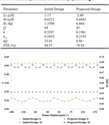
Table 3 details the extracted parameters from simulations between initial design using capacitors as lumped elements and proposed design integrated with capacitor-plates at per-fect alignment.
Comparisons in terms of coupling coefficient and mutual inductance are made between initial and proposed designs under various types of displacement as shown in Fig. 5 till Fig. 7. Even though stability of k and M are observed when receiving resonator is subjected to planar and vertical
TABLE 3.Extracted parameters of initial and proposed design.
FIGURE 5. Simulated coupling coefficient and mutual inductance under planar displacement.
displacements, there are rapid fluctuations of k and M under vertical displacement as compared to the proposed design. List of displacement-tolerant performance comparison is shown in Table 4. Minimal variation ratios of k and kQ indicate link stability with a decreased susceptibility towards coupling variations caused by imperfect alignment between a paired resonators. Variation ratios are computed as VRk =
(kmax–kmin) (kmax)−1and VRkQ=(kQmax–kQmin) (kQmax)−1
respectively. Improvement of the proposed design in compar-ison with initial design can be distinguished from the amount of variation ratio reduction percentages,1VR.
B. EXPERIMENTAL RESULTS
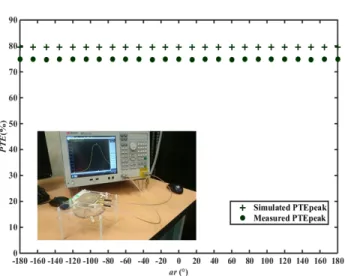
Proposed design is fabricated on a double-sided FR-4 sub-strate with dielectric constant of 4.7 as illusub-strated in Fig. 8. The overall dimension is 66 mm × 70 mm. At ideal orientation in which rotational angle, ar, lateral offset at
x-axis, ax and lateral offset at y-axis, ay are equivalent to zero, the simulated and measured maximum power transfer efficiency achieved are 79.54% and 74.96% respectively. Both simulated and measured reflection and transmission coefficient plots are depicted in Fig. 9. Slight resonance frequency shift is observed from measured results owing to fabrication imperfections.
The experimental setup to assist planar displacement is performed with two acrylic sheets with dimensions of 15 mm by 15 mm by 2 mm and a smaller acrylic sheet with dimen-sions of 10 mm by 10 mm by 2 mm. The first and second dissimilar acrylic sheets is separated by nylon PCB standoffs
FIGURE 6. Simulated coupling coefficient and mutual inductance under lateral displacement (x-axis).
FIGURE 7. Simulated coupling coefficient and mutual inductance under lateral displacement (y-axis).
at 15 mm as shown in the inset of Fig. 10. The receiving res-onator positioned on top of the first acrylic sheet is manually rotated based on a protractor placed on the third acrylic sheet. Measurement tool used is Keysight Vector Network Analyzer (VNA) E5071C applicable for designs with frequency rang-ing from 9 kHz till 6.5 GHz. Measurement results display sustainable PTE which validates the simulated results when receiving resonator is rotated from −180◦to 180◦with step size of 15◦. Average PTE for simulated and measured results are 79.48% and 74.83% respectively.
Tolerance towards displacement caused by both planar and lateral offsets are investigated by deliberately rotating receiving resonator at a specific ar before being moved across
x- and y-axis at various ax and ay in order to emulate prac-tical applications of non-ideal orientations. ar ranges from 0◦to 180◦while lateral displacement quotient ranging from
TABLE 4.Comparison of simulated displacement-tolerant performance.
FIGURE 8. Fabricated printed spiral resonator with capacitive plates: Top (Left); Bottom (Right).
0 till 1 refers to the ratio of lateral shift ax or ay to the axial distance. The corresponding simulated and measure-ment results as well as measuremeasure-ment setups are depicted in Fig. 11 and Fig. 12. Reasonable agreement between sim-ulated and measured results are observed for both plots. Table 5 summarizes displacement-tolerant performance of proposed design. Variation ratio,1VR is used to assess the extent of PTE sustainability and computed as [32]:
1VR(%) = 100 ∗ (PTEpeakmax− PTEpeakmin)
∗(PTEpeakmax)
−1. (11)
Under planar displacement, variation ratio of measured PTE obtained is 0.29% in which PTE is above 70% for all rotational angles from −180◦ till 180◦. Average measured variation ratio for both planar and lateral displacement at
x- and y- axis are 20.14%. For all rotational angles, lateral off-sets of x- and y- axis, measured PTE obtained is above 55%.
L. L. Pon et al.: Displacement-Tolerant Printed Spiral Resonator With Capacitive Compensated-Plates
TABLE 5. Comparison of simulated displacement-tolerant performance.
FIGURE 9. Measurement setup for planar displacement: Top View (Left); Perspective (Right).
FIGURE 10. Comparison of the simulated and measured PTE under planar displacement.
Table 6 shows comparison between the proposed design in this work with other published works related to planar and lateral displacement designs. Most of the published works emphasized on either lateral or planar misalignment
FIGURE 11. Comparison of the simulated and measured peak PTE under planar and lateral displacement (x-axis).
FIGURE 12. Comparison of the simulated and measured peak PTE under planar and lateral displacement (y-axis).
insensitive designs. However, robustness towards planar and lateral offsets at the same instance is not being investigated. As such, proposed design in this work appears to excel by demonstrating satisfactory planar and concurrent planar with lateral offsets aside from simplicity and hassle-free design.
TABLE 6. Comparison with published works.
IV. CONCLUSION
A novel printed spiral resonator with series-parallel capac-itive compensated plates on a single printed circuit board is presented. Without any displacement where ar, ax and
ay are equivalent to zero, maximum simulated and mea-sured transfer efficiency of 79.54% and 74.96% are achieved. Assessment on the endurance towards planar displacement at z-axis, lateral displacement at x- and y-axis as well as concurrent lateral and planar displacement are performed. Variation ratio of transfer efficiency is computed at 0.29% for planar displacement. Measurement results are substantiated with the capability of robustness towards displacement when the average variation ratio for concurrent types of offsets is found to be 20.14%. With a minimized and flattened footprint of 66 mm × 70 mm × 0.4 mm, sustainable power transfer efficiency featuring tolerable displacement restraints in addi-tion to straightforward assembly and cost-conscious design is demonstrated for non-radiative low-power wireless energy transfer application.
REFERENCES
[1] S. Y. Hui, ‘‘Planar wireless charging technology for portable electronic products and Qi,’’ Proc. IEEE, vol. 101, no. 6, pp. 1290–1301, Jun. 2013. [2] M. Song, P. Belov, and P. Kapitanova, ‘‘Wireless power transfer inspired by the modern trends in electromagnetics,’’ Appl. Phys. Rev., vol. 4, p. 021102, Jun. 2017.
[3] Z. Li, W. Cheng, J. Yi, and J. Li, ‘‘Design and optimization of quasi-constant mutual inductance for asymmetric two-coil wireless power trans-fer system with lateral misalignments,’’ Prog. Electromagn. Res. M, vol. 69, pp. 207–217, Jun. 2018.
[4] X. Mou, O. Groling, and H. Sun, ‘‘Energy-efficient and adaptive design for wireless power transfer in electric vehicles,’’ IEEE Trans. Ind. Electron., vol. 64, no. 9, pp. 7250–7260, Sep. 2017.
[5] F. Jolani, Y.-Q. Yu, and Z. D. Chen, ‘‘Electromagnetic modeling and opti-mization of magnetic resonant coupling wireless power transfer using coil array,’’ in Proc. IEEE MTT-S Int. Conf. Numerical Electromagn. Multiphys.
Modeling Optim. (NEMO), vol. 1, Aug. 2015, pp. 1–3.
[6] U.-M. Jow and M. Ghovanloo, ‘‘Geometrical design of a scalable overlap-ping planar spiral coil array to generate a homogeneous magnetic field,’’
IEEE Trans. Magn., vol. 49, no. 6, pp. 2933–2945, Jun. 2013.
[7] S. Wang, Z. Hu, C. Rong, C. Lu, J. Chen, and M. Liu, ‘‘Planar multiple-antiparallel square transmitter for position-insensitive wireless power transfer,’’ IEEE Antennas Wireless Propag. Lett., vol. 17, no. 2, pp. 188–192, Feb. 2018.
[8] A. L. A. K. Ranaweera, C. A. Moscoso, and J.-W. Lee, ‘‘Anisotropic metamaterial for efficiency enhancement of mid-range wireless power transfer under coil misalignment,’’ J. Phys. D, Appl. Phys., vol. 48, no. 45, p. 455104, 2015.
[9] D. Liu, H. Hu, and S. V. Georgakopoulos, ‘‘Misalignment sensitivity of strongly coupled wireless power transfer systems,’’ IEEE Trans. Power
Electron., vol. 32, no. 7, pp. 5509–5519, Jul. 2017.
[10] S. Hekal, A. B. Abdel-Rahman, H. Jia, A. Allam, A. Barakat, and R. K. Pokharel, ‘‘A novel technique for compact size wireless power trans-fer applications using defected ground structures,’’ IEEE Trans. Microw.
Theory Techn., vol. 65, no. 2, pp. 591–599, Feb. 2017.
[11] A. Barakat, K. Yoshitomi, and R. K. Pokharel, ‘‘Design approach for effi-cient wireless power transfer systems during lateral misalignment,’’ IEEE
Trans. Microw. Theory Techn., vol. 66, no. 9, pp. 4170–4177, Sep. 2018. [12] S. Mehri, A. C. Ammari, J. B. H. Slama, and M. Sawan, ‘‘Design
optimiza-tion of multiple-layer PSCs with minimal losses for efficient and robust inductive wireless power transfer,’’ IEEE Access, vol. 6, pp. 31924–31934, 2018.
[13] T. C. Beh, M. Kato, T. Imura, S. Oh, and Y. Hori, ‘‘Automated impedance matching system for robust wireless power transfer via magnetic resonance coupling,’’ IEEE Trans. Ind. Electron., vol. 60, no. 9, pp. 3689–3698, Sep. 2013.
[14] J. Kim, D.-H. Kim, and Y.-J. Park, ‘‘Free-positioning wireless power transfer to multiple devices using a planar transmitting coil and switchable impedance matching networks,’’ IEEE Trans. Microw. Theory Techn., vol. 64, no. 11, pp. 3714–3722, Nov. 2016.
[15] J. L. Villa, J. Sallan, J. F. S. Osorio, and A. Llombart, ‘‘High-misalignment tolerant compensation topology for ICPT systems,’’ IEEE Trans. Ind.
Electron., vol. 59, no. 2, pp. 945–951, Feb. 2012.
[16] A. A. Eteng, S. K. A. Rahim, C. Y. Leow, B. W. Chew, and G. Vandenbosch, ‘‘Simple compensation for lateral misalignments in resonant inductive coupling links,’’ Electron. Lett., vol. 52, pp. 954–956, May 2016. [17] A. A. Eteng, S. K. A. Rahim, and C. Y. Leow, ‘‘Geometrical enhancement
of planar loop antennas for inductive near-field data links,’’ IEEE Antennas
Wireless Propag. Lett., vol. 14, pp. 1762–1765, 2015.
[18] A. A. Eteng, S. K. A. Rahim, C. Y. Leow, B. W. Chew, and G. A. E. Vandenbosch, ‘‘Two-stage design method for enhanced inductive energy transmission with Q-constrained planar square loops,’’ PLoS ONE, vol. 11, p. e0148808, Feb. 2016.
[19] S. S. Mohan, M. del Mar Hershenson, S. P. Boyd, and T. H. Lee, ‘‘Simple accurate expressions for planar spiral inductances,’’ IEEE J. Solid-State
L. L. Pon et al.: Displacement-Tolerant Printed Spiral Resonator With Capacitive Compensated-Plates
[20] U.-M. Jow and M. Ghovanloo, ‘‘Modeling and optimization of printed spiral coils in air and muscle tissue environments,’’ Proc. 31st Annu. Int.
Conf. IEEE Eng. Med. Biol. Soc., Eng. Future Biomed. (EMBC), Sep. 2009, vol. 3, no. 5, pp. 6387–6390.
[21] U.-M. Jow and M. Ghovanloo, ‘‘Design and optimization of printed spiral coils for efficient transcutaneous inductive power transmission,’’ IEEE
Trans. Biomed. Circuits Syst., vol. 1, no. 3, pp. 193–202, Sep. 2007. [22] Z. Liu, Z. Zhong, and Y. X. Guo, ‘‘Rapid design approach of optimal
efficiency magnetic resonant wireless power transfer system,’’ Electron.
Lett., vol. 52, no. 4, pp. 314–315, 2016.
[23] K. A. Thackston, H. Mei, and P. P. Irazoqui, ‘‘Coupling matrix synthesis and impedance-matching optimization method for magnetic resonance coupling systems,’’ IEEE Trans. Microw. Theory Techn., vol. 66, no. 3, pp. 1536–1542, Mar. 2018.
[24] G. K. Felic, D. Ng, and E. Skafidas, ‘‘Investigation of frequency-dependent effects in inductive coils for implantable electronics,’’ IEEE Trans. Magn., vol. 49, no. 4, pp. 1353–1360, Apr. 2013.
[25] H.-M. Hsu, ‘‘Improving the quality factor of a broadened spiral induc-tor with arithmetic-progression step width,’’ Microw. Opt. Technol. Lett., vol. 45, pp. 118–120, Apr. 2005.
[26] N. Inagaki, ‘‘Theory of image impedance matching for inductively coupled power transfer systems,’’ IEEE Trans. Microw. Theory Techn., vol. 62, no. 4, pp. 901–908, Apr. 2014.
[27] G. Vandevoorde and R. Puers, ‘‘Wireless energy transfer for stand-alone systems: A comparison between low and high power applicability,’’ Sens.
Actuators A, Phys., vol. 92, pp. 305–311, Aug. 2001.
[28] T. Ohira, ‘‘What in the world is Q?’’ IEEE Microw. Mag., vol. 17, no. 6, pp. 42–49, Jun. 2016.
[29] T. Ohira, ‘‘The kQ product as viewed by an analog circuit engineer,’’ IEEE
Circuits Syst. Mag., vol. 17, no. 1, pp. 27–32, 1st Quart., 2017.
[30] T. Imura and Y. Hori, ‘‘Maximizing air gap and efficiency of magnetic resonant coupling for wireless power transfer using equivalent circuit and Neumann formula,’’ IEEE Trans. Ind. Electron., vol. 58, no. 10, pp. 4746–4752, Oct. 2011.
[31] A. Karalis, J. D. Joannopoulos, and M. Soljačić, ‘‘Efficient wireless
non-radiative mid-rangeenergy transfer,’’ Ann. Phys., vol. 323, pp. 34–48, Jan. 2008.
[32] A. A. Eteng, S. K. A. Rahim, C. Y. Leow, and H. A. E. Elobaid, ‘‘Method to reduce distance-sensitivity within an operating range in HF-RFID WPT links,’’ in Proc. IEEE 10th Eur. Conf. Antennas Propag. (EuCAP), Apr. 2016, pp. 1–4.
LAI LY PON (S’08) received the B.Eng. (Electrical) and M.Eng. (Electrical) degrees from Universiti Teknologi Malaysia (UTM), in 2007 and 2010, respectively, where she is cur-rently pursuing the Ph.D. degree with the Wireless Communication Centre. She has spent five years working in various companies in the telecommu-nication industry. Her research interests include near field wireless energy transfer; metamaterial, wireless propagation, and mobile network system.
SHARUL KAMAL ABDUL RAHIM received the degree in electrical engineering from The Univer-sity of Tennessee, Knoxville, TN, USA, the M.Sc. degree in engineering (communication engineer-ing) from Universiti Teknologi Malaysia (UTM), and the Ph.D. degree in wireless communication system from the University of Birmingham, U.K., in 2007. After his graduation from The University of Tennessee, he spent three years in industry. After graduating the M.Sc. degree, he joined UTM in 2001, where he is currently a Professor with the Wireless Communication Centre. He has published over 200 learned papers in journals, including the IEEE Antenna and Propagation Magazine, the IEEE TRANSACTIONS ON
ANTENNA ANDPROPAGATION, the IEEE ANTENNA ANDPROPAGATIONLETTERS, and
has many patents. His research interests include antenna design, smart antenna system, beamforming network, and microwave devices for fifth gen-eration mobile communication. He is a Senior Member of the IEEE Malaysia Section, a member of the Institute of Engineer Malaysia, a Professional Engineer with BEM, a member of the Eta Kappa Nu Chapter, University of Tennessee, and the International Electrical Engineering Honor Society. He is currently an Executive Committee member of the IEM Southern Branch.
CHEE YEN LEOW (S’08–M’12) received the B.Eng. degree in computer engineering from Universiti Teknologi Malaysia (UTM), Johor Bahru, Malaysia, and the Ph.D. degree from Imperial College London, U.K., in 2007 and 2011, respectively. Since 2007, he has been an Academic Staff with the School of Electrical Engineering, Faculty of Engineering, UTM. He is currently an Associate Professor with the Faculty and a Research Fellow at the Wireless Communication Centre (WCC), Higher Institution Centre of Excellence, UTM, and the UTM-Ericsson Innovation Centre for 5G. His research interests include non-orthogonal multiple access, cooperative communication, UAV communica-tion, MIMO, hybrid beamforming, physical layer security, wireless power transfer, convex optimization, game theory, and prototype development using software-defined radio for 5G and IoT applications.
MOHAMED HIMDI received the Ph.D. degree in signal processing and telecommunications from the University of Rennes 1, Rennes, France, in 1990. Since 2003, he has been a Professor with the University of Rennes 1, and the Head of the High Frequency and Antenna Department, Institute d’Electronique et Telecommunications de Rennes, until 2013. He has authored and co-authored 110 journal papers, over 250 papers in conference proceedings, and nine book chap-ters. He holds 38 patents in the area of antennas. His research activities concern passive and active millimeter-wave antenna. His research inter-ests also include theoretical and applied computational electromagnetics, development of new architectures of printed antenna arrays, and new three-dimensional (3D) antenna technologies. He was a recipient of the 1992 International Symposium on Antennas and Propagation Conference Young Researcher Scientist Fellowship, Japan, and has received an Award presented by the International Union of Radio Scientist, Russia, in 1995. He was a Laureate of the Second National Competition for the Cre-ation of Innovative Company, Ministry of Industry and EducCre-ation, France, in 2000 and 2015. In 2015, he received the JEC-AWARD-10 at Paris for Pure composite material antenna embedded into a motorhome roof for the Digital Terrestrial Television reception.
MOHSEN KHALILY (M’13–SM’18) was with the Wireless Communication Center, Universiti Teknologi Malaysia (UTM), as a Senior Lec-turer, and as a Postdoctoral Research Fellow, from 2012 to 2015. He joined the Institute for Commu-nication Systems (ICS), home of 5G Innovation Centre, University of Surrey, U.K., as a Research Fellow on antenna and propagation, since 2015. His research interests include dielectric resonator antennas, MIMO antennas, phased array anten-nas, hybrid beamforming, and millimetre-wave antennas and propagation. He is a member of the IEEE Antennas and Propagation Society, the IEEE Communication Society, the IEEE Microwave Theory and Techniques Soci-ety, an Associate Editor for the IEEE ACCESS, and has published almost 70 academic papers in international peer-reviewed journals and conference proceedings.